Note: Descriptions are shown in the official language in which they were submitted.
;~lr~
P~IN 13696 1 15.a4.1992
Method of manufacturing a semiconductor device comprising a capacitor with a
ferroelectric dielectric, and semiconductor device comprising such a capacitor.
Ille invention relates to a method of manufactuIing a ~emiconductor
device whereby a capacitor is provided on a surface of a semiconductor body
comprising a semiconductor elernent in that consecutively a lower electrode, an oxidic
ferroelectric dielectric, and an upper electrode are provided in such a way that the
5 upper electrode does not cover an edge of the dielectric, after which an insulating layer
with superimposed metal conductor tracks is provided. The invention also relates to a
semiconductor device comprising a capacitor with a ferroeleetric dielectric.
Such a method is suitable for manufacturing a semiconductor device
which can operate, for example, as an electronic memory in a computer. The
10 semiconductor body then comprises very many semiconductor elements and capacitors.
Capacitors having a ferroelectric material as a dielectric form non-volatile memory
elements. When an electric field is applied across a ferroelectric material and removed
again, a permanent polari~ation of the mateIial remains, depending on a direction of the
electric field, i.e. the ferroelectric material remembers the dire~tion of the electric
15 field. Especially oxidic materials such as, for e~ample, lead titanate, lead-lanthanum
titanate, and lead-lanthanum-zirconium ~tanate exhibit ferroelect~ic properties.
European Patent Applica~ion 91200525.3 (PHN 13.274~ discloses a
20 method of the Idnd mentioned in the opening paragraph wher~by a capacitor with a
lower electrode comprising platinum, a ferroelectric dielectric, and an upper electrode
comprising platinum are provided on a semiconductor body. Lead-zirconium ~tanate is
used as the ferroelectric dielectric in that case. The sen~iconductor body also comprises
a switching transistor which is connected to the capacitor ~ a metal conductor track of
;,,
.. . ..
: : , ~. , , , . .
.
PEIN 13696 ~ 15.04.1992
TiW and Al which is provided over an insulating layer of silicon oxide.It is found in practice that a device manu~actured by the known method
described is comparatively slow and, for example, shows an access time which is
longer than 100 nsec.
s
The invention has for its object inter alia to provide a method by which
a device with a shorter access time is made.
According to the invention, the method mentioned in the opening
10 paragraph is ~or this purpose characterized in that the edge of the upper electrode not
covered by the dielectric is covered with a coating layer which is practically
imperviable to hydrogen, and in that then the device is heated in an atmosphere which
contains hydrogen.
It is found that the manufacture of a device by the known method leads
lS to free or "dangling" bonds being forrned in a surface layer of the insulating layer
when the metal conductor track is formed on this layer. In the known method, thedevice cannot be heated in an atmosphere containing hydrogen in a usual manner in
order to bind these dangling bonds with hydrogen and thus to neu~aliæ them. In faet,
the oxidic ferroelec~ic mateAal would also be heated in an atn osphere containing
20 hydrogen then and be reduced to form an electrically conducting material. By covering
the edge of the dielectric not covered by the upper electrode with a coating layer which
is practically imperviable to hydrogen before heating in an atmosphere containing
hydrogen, upon which heating takes place in an atmosphere containing hydrog~n, the
dangling bonds OEe neutralized. As the coa~ng layer, for example, a silicon nitride or a
25 silicon oxynitride layer is provided. The access times of appro~imately 100 nsec rnay
then be reduced to less than 25 nsec.
A small quantity of hydrogen may diffuse through the upper electrode
and reduce the ferroelectric dielectric situated below ~he upper electrode.
An upper electrode made of an oxidic conductor such as LaO 5SrO 5CoO3 may also be
30 used. Such an upper ele trode could also be attacked by the hydrogen. Preferably,
therefore, the coa~ng layer is provided over substantially the entire upper electrode.
.
,
3~ 3
PHN 13696 3 15.04.1992
Preferably, the method according to the invention is characteriæd in that
a silicon nitride layer is provided as the coating layer. Silicon nitride forms a very good
barrier against hydrogen, while silicon nitride is often use<l in practice as a passivating
layer over an en~re semiconductor device, the: equipment necessary for this being
5 available. In addition, silicon nitride can be very well selectively etched relative to
silicon oxide, so that silicon nitride can be easily brought into a pattern whereby silicon
nitride can be provided only at the area of the capacitor. The provision of the silicon
nitride may be effected by a known technique such as, for example, deposition from a
gas phase (CVD). Especially silicon nitride provided at a temperature of approximately
lû 8~) C forms a very good barrier against hydrogen.
An additional advantage is obtained when a layer of silicon oxide is
provided bet~veen the silicon nitride layer and the surface of the semiconductor body.
Mechanical stresses can occur in ehe silicon nitride, causing cracks or shifts in
conductor tracks or electrodes of the capacitor. A silicon o~de layer is capable of
15 absorbing these stresses, so that the conductor tracks and the electrodes remain intact.
The silicon oxide layer may be provided in a known manner (for example, in a 1 atm.
SILOX process~, possibly supported by a plasma (PECVD).
A further embodiment is characterized in that a hydrogen-absorbing layer
is provided as ~e coating layer. A layer of, for example, nickel or palladium may be
20 provided as the hydrogen-absorbing layer. This layer may also seIve as a conductor
track. The absorbing layer must have such a thichless that only a very small quantity
of hydrogen can penebate the ferroelectric dielectric duling hea~ng in the hydrogen
atmo~here.
Preferably, palladium is provided as the hydrogen-absvrbing layer.
25 Palladium absorbs hydrogen well, while it is also easily provided, for example, by a
sputtering process.
If a conducting hydrogen-absorbing layer is used, the capacitor may be
short-circuited. Preferably, an insulating auxiliary layer is provided between the
hydrogen-absorbing layer and the surface of the semiconductor body. The provision of
30 the insulating auxiliary layer means that the conducting hydrogen-absorbing layer need
not necessarily be removed and can even be used as an additional conductor track.
~ , . ~ , .
-: . . ..
,.~
3~
PHN 13696 ~ 15.04.1992
Preferably, a silicon nitride layer is provided as the auxiliary layer by
means of a plasma enhanced de~osition process from the gas phase (Plasma ~nhanced
Chemical Vapour Deposition, PECVD). PECVl:) silicon nitride is provided at a
comparatively low temperature of between approximately 200 and 350 C, so that the
5 influence of the temperature on the serli~conductor device is small. Silicon nitride
provided by means of PECVD, however, contains a quantity of hydrogen. During
heating of the semiconductor device, this hydrogen can diffuse into the ferroelectric
dielectric and cause a degradation of this dielectric. Ille absorption layer absorbs
hydrogen from the silicon nitIide layer and thus ensures a low hydrogen pressure in the
10 silicon nitride, so that the hydrogen will not diffuse fr~m the silicon nitride layer into
the ferroelectric dielectric. In addition, the transmissivity of the silicon nitride layer for
hydrogen is small.
The invention also relates to a semiconductor device comprising a
serniconductor body with a semiconductor element and a surface on which is present a
15 capacitor with a lower electrode, an oxidic ferroelectric dielectric, and an upper
electrode which does not cover an edge of ~he dielectric, an insulating layer with
superimposed metal conductor tracks being provided on the semiconductor body.
According to the invention, said device is characterized in that a coating layer which is
practically imperviable to hydrogen is provided at the area of the said edge. Such a
20 serniconductor device can be heated in a hydrogen-con~aining atmosphere in order to
reduce its access time without the oxidic ferroelec~ic dieleetric being attacked.
Dur~ng heating in a hydrogen-containing atmosphere, a small quantity of
hydrogen can diffuse through the upper electrode and reduce the ferroelectric dielectric
situated below the upper electrode. Preferably, therefore, the coating layer is provided
25 over substantially the entire upper electrode.
Pref~rably, the device according to the invention is characteri~ed in that
a silicon nitride layer is provided as the coa~ng layer. Silicon r~itride forms a very good
barIier against hydro,gen, while silicon nitride is often used in practice as a passivating
layer over an entire sRmiconductor device, the equipment necessary for this being
30 available. In addition, silicon nitride can be very well selectively etched relative to
silicon oxide. The provision of the silicon nit~ide can take place by a known technique
.
PHN 1369~ ~ 15.04.1992
such as, for example, deposition from a gas phase (CVD). Especially silicon nitride
provided at a temperature of approximately 8~0 C forms a very good barrier against
hydrogen, so that the semiconductor device c,an be heated in a hydrogen-containing
atmosphere.
S An additional advantage is obtained when a layer of silicon oxide is
provided between the silicon nitride layer and the surface of the semiconductor body.
Mechanical stresses can occur in the silicon nitride, causing cracks or shifts in
conductor tracks or capacitor electrodes. A layer of silicon oxide is capable ofabsorbing these stresses, so that the conductor tracks and the electrodes remain intact.
A further embodiment is characte~ized in that a hydrogen-absorbing layer
is provided as the coating layer. A layer of, for example, nick~l or palladium may be
provided as the hydrogen-absorbing layer. The semiconductor device can then be
heated in a hydrogen-conta~ning atmosphere without the oxidic ferroelectric dielectric
being attacked. The said layer may also serve as a conductor track. The absorbing layer
must have such a thickness that only a very small quan~ty of hydrogen can penetrate
the ferroelectric dielectric during heating in the hydrogen-containing atmosphere.
Preferably, palladium is provided as the hyd~ogen-absorbing layer.
Palladium absorbs hydrogen well, while i~ is also easily provided, for example, by a
sputtering process.
If a conducting hydrogen-absorbing layer is used, the capacitor may be
short-circuited. Preferably, an insulating auxiliary layer is provided b tween the
hydrogen-absorbing layer and the surface of the semiconductor body. Thanks to this
insulating au~iliary layer, the absorbing layer may be used as an additional conductor
track.
Preferably, a silicon nitride layer is provided as the au~iliary layer by
means of a plasma enhanced deposition process from the gas phase (Plasma Enhanced
Chernical Vapour Deposition, PECVD). PECVD silicon nitride is provided at a
comparatively low temperature of behveen approximately 200 and 350 C, so that the
influence of the temperature on the semiconductor device is small. Silicon ni~ide
30 provided by means of PECVD, however, contains a quan~y of hydrogen. During
heating of the semiconductor device, this hydrogen can diffilse into the ferroelec~ic
t
6~C~
PEIN 13696 6 15.04.1992
dielectric and cause a degradation of this dielectric. The absorption layer absorbs
hydrogen from the silicon nitride layer and thus ensures a low hydrogen pressure in the
silicon nitride, so that the hydrogen will not diffuse from the silicon nitride layer into
the ferroelectric dielectric. In addition, ehe ~ansmissivity of the silicon nitride layer for
hydrogen is small.
The invention will be explained in more detail below by way of example
with reference to drawings, in which:
Fig. 1 is a cross-section of a semiconductor device having a capacitor at
a surface comprising a ferroelectric dielectric provided with a coating layer according
to the invention,
Figs. 2 to 5 are cross-sections of serniconductor devices, each having a
capacitor at a surface with a ferroelectric dielectric provided with a coating layer
according to further embodiments of the invention.
The Figures are purely diagrarnmatic and not drawn to scale.
Corresponding parts are generally given the same reference numerals in the Figures.
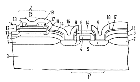
Fig. 1 shows a cross-section of a sen~iconductor device made according
to the invention. In the method aecording to the invention, a semiconductor device is
manufactured in that a capacitor 2 is provided 031 a sur~ace 10 of a semiconductor body
3 comprising a semiconductor element 1 through the provision of a lower eleckode 11,
an oxidic ferroelectric dielectric 12, and an upper elec~ode 13 in that order, the upper
electrode not covering an edge of the dielectric, after which an insula~ng layer 14 with
superim~Dsed metal conductor tracks 17 and 18 is provided. Such a semieonductor
device forms a memory element with switching elec~onics. For that purpDse, a
serniconductor element 1 acting as a switching ~ansistor is connected to a capacitor 2.
Only one transistor 1 and one capacitor 2 are drawn for simplity's sake, but in practice
30 the semiconductor body 3 comprises ve~y many such transistors and capacitors. The
MOS transistor is pnDvided in usual manner in the silicon semiconductor body 3 with a
P~IN 13696 7 15.0~.1992
gate electrode 4 of polycrystalline silicon insulated from the semiconductor body 3 by a
silicon oxide layer S having a thickness of approximately 30 nm. The gate electrode 4
is further insulated by means of a silicon o~ide layer 6. Different transistors are
separated from one another by field oxide regions 7. Source and drain regions 8 and 9
S of the transistor are made through diffusion between field oxide 7 and gate electrode 4.
The semiconductor filrther comprises the surf~lce 10 on which the capacitor 2 forming a
memory element is provided in known manner wit}l a lower elec~ode 11 comprising
platinum, a ferroelectric dielectric 12, and an upper electrode 13 comprising platinum.
The lower electrode 11 is provided, for example, through a sputtering process on a Si
10 < 100> slice 3, which is provided with an approximately 600 nm thiclc layer of SiO2 6
in that a 20 nm thick layer of titanium is deposited, a 39 nm thick layer of platinum is
deposited, and then S nm titanium is deposited again, upon which the lower electrode is
heated for one hour at 750 C in an N2/O2 4: 1 atrnosphere. A lower electrode with a
thichless of approximately 75 nm and comprising platinum is then present with good
15 adhesion on the semiconductor surfaca The square resistance is approximately 4 Q.
The lower electrode has a roughness of approximately 0,01 ~m.
After the lower electrode has been provided, the ferroelectric dielectric 1~, for example
lead-zirconium titanate, is provided on the elec~ode material 11. The starting material
for this is a solution of lead ethylhexanoate, zirconium acetylacetonate and titanium-n-
20 butoxide in n-butanol (molar concentrations appro~imately 0,2-0,5). This solution is
provided on the lower electrode by means of a spinning process in a centrifuge
(rotation speed approximately 500-1500 rpm). 13aking takes place at approximately
700 C for 6 hours in a furnace with an NJO2 4: 1 atmosphere. The layer thichless of
the ferroelectric material obtained by one spinning process and one b~dng cycle is
25 appro~imately û,l ~m. To obtain a desir~d layer ~hickn~ss of appro;cima~ely 0,S ~m,
this process is ~ed out five times. A typical composition of lead-~irconium titanate
obtained by the process indicated above is PbZrO47TiO 5303.
The lower electrode :ll and the dielectric 12 are then etched into a pattern.
An upper electrode 13 is provided on the ferroelectric dielectric 12 in the same way as
30 the lower electrode 11, except for the hea~ng step, which take3 place at the baldng
temperature of the dielectric, so at approximately 700 C.
. .
,
: ~ ~
PHN 13696 ~ 15.04.1992
The surface of the capacitor 2 is then coated with an insulating layer 14. Contact holes
15 and 16 are etched in this layer. The upper electrode 13 is connected to the source
region 8 of the transistor 1 through these contact holes by means of metal conductor
tracks 17 and 18. For example, a usual alloy of titanium and tungsten is provided as
S layer 17, and an aluminium alloy as layer 18.
The transistor 1 and the capacitor 2 are connected to swit~hing electronics in the
semiconductor body. The lower electrode 11 1s connected to a drive line, the gate
electrode 4 to a word line, while the drain region 9 is connected to a s~called bit line
through me~l conductor tracks 17 and 18. It is possible to drive the rnemory element
10 by means of voltage pulses at the various lines and to switch the ferroelectric dielectric
12 to and fro between two stable polarization states.
It is found in practice that a device made by the known method desc~ibed
is comparatively slow and has an access time which is, for example, longer than 100
nsec.
lS To manufacture a faster device, accoIding to the invention, the method
mentioned in the opening paragraph is characterized in that the edge of the upper
electrode not covered by the dielectric is covered with a coating layer which ispractically imperviable to hydrogen, and in that then the device is heated in anatmosphere which contains hydrogen.
20 A device made by the known method is comparatively slow because dangling bonds are
present below conductor tracks. These bonds may easily release electrons and thus
affect the charge ~ansport through the conductor tracks, which renders the device slow.
The dangling bonds aIise during the deposition of the metal of the conductor tracks on
the region of insulating material. To obtain a good adhesion9 a metal which reduces the
25 insulating material is used, for example titanium or alumil~ium, whereby dangling
bonds are created. These bonds are neutralized by a heat treatment at approximately
450 C in an atmosphere containing hydrogen during appro~imately 30 minutes.
During the heat treatment, the hydrogen dif~ses through the insulating layer or through
the conductor tracks and chemi~ally joins itself to the dangling bond, so that the
30 dangling bond is neu~halized. The charge transport through the conductor tracks is then
no longer hampered, which renders the device faster. A disadvantage of the heat
:
PHN 13696 9 15.04.1992
treatment in an atmosphere containing hydrogen is that the oxidic ferroelectric
dielectric is also reduced by the hydrogen anld thus loses its ferroelectric characteristics.
In particular, hydrogen diffuses to the dielec~lic through the edge not covered by the
upper electrode. To prevent the penetration cf hydrogen into the ferroelectric dielectric,
5 according to the invention, a coating layer wlhich is practically imperviable to hydrogen
is provided at the area of the edge. The insulating layer 14 in Fig. 1, for example, may
be provided to form such a coating layer. It is alternatively possible to provide a
separate coating layer over the non-covered e~ge of the capacitor. The coating layer
may be, ~or example, a silicon nitride or silicon oxynitride layer provided by a usual
10 deposition process from the gas phase (CVD).
By way of example, a silicon nitride layer is provided over the upper electrode 13
comprising platinum of the capacitor 2 in that silane and ammonia are made to react ~n
usual manner in a deposition reactor at approximately 700 C. An approximately 11
~m thick insulating layer 14 of silicon nitride ls then provided, for example. Such a
15 silicon nitride layer contains up to approximately 8 at% hydrogen. This quantity,
howeYer, is not high enough to cause damage to the dielectric.
Contact holes 15 and 16 are etched in the silicon nitride layer previously provided,
upon which a 100 nm thick layer 17 of a titanium-tungsten alloy (for exarnple Ti20W80)
is provided through a sputtering process, followed by a 500 nm thick layer 18 of20 alurninium. I)angling bonds are present at the inter~ace between the silicon nitride layer
14 and the titanium-tungsten layer 17, which bonds are neut~alized by a heat treatment
of appro~imately 30 n~inutes at 450 C in an atmosphere containing hydrogen (forexample, N2/H2 4: 1). The silicon nitride layer 14 then forrns an effective ba~ier
against the hydrogen, so that the ferroelectric dielectric is not reduced during the
25 neutralization of the dangling bonds.
The upper electrode in the known device is made of pla~num, possibly
provided with a titanium adhesion layer. A small quanti~y of hydrogen may diffuse
through the upper electrode, for example at the contact hole 15, and reduce the
ferroelectric dielec~ie 12 situated below the upper electrode 13. This may lead to a
30 change in the capacitance value of the capacitor, since the reduc~on of a ferroelectIic
dielectric by hydrogen leads to the creation of a conductive layer, which reduces the
~ : ,
~',., '
,
P~N 13~96 10 15.04.19g2
thickness of the dielectric or even completely short-circu;ts the capacitor. It is also
possible for an upper electrode made of an oxidic conductor to be used, such as, for
example, LaO5SrO5CoO3, which can be attack~ by the hydrogen. Preferably, therefore,
the coating layer is provided over substantially the entire upper electrode. Fig. 2 shows
S a semiconductor device in which the capacitor 2 is provided with a lower electrode 11,
a ferro~lectric dielectric 12 which fully covers the lower electrode 11, and an upper
electrode 13 which forms a connection to a conductnr tMclc of titanium 17 and
aluminium 18. The upper electrode 13 is fully covered by a coating layer 20 which is
practically imperviable to hydrogen, so that during a heat treatment of the device in an
10 atmosphere containing hydrogen substantially no hydrogen can penetrate the dielectric.
A silicon nitride layer with a thickness of approximately 300 nm is preferably provided
as the coating layer 14 or 20 practically imperviable to hydrogen. Silicon nitride forms
a very good barrier against hydrogen because of its high density. In practice, silicon
nitride is often used as a passivating layer over an entire semiconductor device, so that
15 the necessary deposition equipment is available. In addition, silicon nitnde can be very
well selectively etched relative to silicon oxide by means of a wet etching step with
phosphoric acid of 140 C. The silicon nitride may be p~ovided by a ~own technique
such as, for exarnple, deposition from a gas phase (CVD).
In Fig. 3, a layer of silicon oxide 25 with a thickness of 50 nm is
20 provided over the upper electrode 13, over which again the silicon nitride layer 20 of
300 nm thickness is provided. An additional advantage is obtained in this way, since
mechanical stresses which may occur in the silicon n~kide and which may cause cracks
or shifts in conductor traeks or electrodeg of the capacitor are reduced.
A further embodiment preferably comprises a hydrogen-absorbing layer
25 30 (see ~ig. 4) as the coating layer. A layer of, for example, nickel or palladium may
be used as the hydrogen-absorbing iayer. These layers may be provided by means of
usual techniques such as CVD or sputtering. In Pig. 4, a palladium layer is provided
over the upper electr~de 13 of the capacitor by way of hydrogen-absorbing layer 30.
This layer may also be used as an additional conductor track, as shown in Pig. 4. The
30 palladium layer may be covered in usual manner by, ~ur example, a silicon oxide layer
4û. Palladium absorbs hydrogen well, while it is also easy to provide, for example, by
. ~ -
,.
~ ~ .
PHN 13696 11 15.04.1992
a sputtering process. The absorbing layer must have such a thickness that only a very
small quantity of hydrogen can penetrate the ferroelectric dielectric during heating in
the hydrogen atmosphere, for exa nple, a thickness of 0,2 ~m palladium for a heat
treatment of 30 minutes at 450 C. The palLIdium layer may short-circuit the capacitor,
S which is why preferably first an insulating auxiliary layer 50 of silicon oxide or silicon ~.
nitride is provided be~ore the hydrogen-absorbing layer 30 is provided (see Fig. 5).
Preferably, a silicon nitride layer provided by means of a plasma enhanced deposition
process from the gas phase ~PECVD) is used for the lay~r 50. Such a layer may beprovided at a comparatively low ternperature of between 200 and 350 C, so that the
10 temperature load on the semiconductor device is small. The palladium layer 30 may
then be fmished again, for example, with a silicon oxide layer 40, for example, a
PECVD oxide layer.
,
- - ..