Note: Descriptions are shown in the official language in which they were submitted.
20 68 186 a~.
- 1 - 41PR-6470
LOAD CURRENT COMMUTATION CIRCUIT
BACKGROUND OF THE INVENTION
Applicant':> U.S. Patent No. 4,636,907, issued
January 13, 198'7, entitled "Arcless Circuit
Interrupter" in the name of E. K. Howell and assigned
to the assignee of the subject application. The
s above referenced U.S. Patent relates to modifying,
i.e. interrupting, load current flow in a first
circuit that ini~erconnects a source of electrical
energy and a load circuit. Load current flowing
through the fir;~t circuit is temporarily diverted to
io a second, i.e. diversion, circuit. Upon load current
diversion, a swatch in the first circuit can be
rapidly opened under substantially zero current
conditions and i:hus without arcing. Diversion of the
load current prior to switch opening is accomplished
i5 by a controlled impedance circuit in the first
circuit. The switch and the controlled impedance
circuit are serially connected between the source of
electrical energy and the load circuit, and the
diversion circuit is connected in parallel with the
2o series combinat_Lon of the switch and the controlled
2088186
- 2 - 41PR-6470
impedance circuit. Various types of diversion
circuits may be utilized for this purpose.
Representative diversion circuits are, for example,
disclosed in the following U.S. Patents which are in
s the name of E. fit. Howell, the subject applicant, and
are assigned to the assignee of the subject
application, U.S. Patent No. 4,700,256, issued
October 13, 198'7 entitled "Solid State Current
Limiting Circuits Interrupter" and U.S. Patent No.
io 4,631,621, issuesd December 23, 1986, entitled "Gate
Turn Off Contro=L Circuit".
Load current diversion to the diversion circuit
is produced by t:he controlled impedance circuit.
During normal operation, i.e., prior to diversion,
15 the controlled impedance circuit essentially has a
very low voltage drop and thus low power dissipation.
Load current di~rersion results from a control signal
which effective:Ly increases the voltage drop across
the controlled :impeda.nce circuit. This voltage
2o causes the tran;~fer of the load current and of energy
stored in the inductive components of the first
circuit to the c3iver~;ion circuit. This is, for
example, furthe:r described in U.S. Patent No.
4,723,187, issuf~d February 2, 1988, entitled "Current
2s Commutation Cir~~uit", which is also in the name of E.
K. Howell, and is asp>igned to the assignee of the
subject applicavion.
Controlled impedance circuits used for load
current diversion must meet various requirements. When
3o switched to their high impedance state, load current
- 3 - 41PR-6470
flow must produce a voltage drop that is sufficient to
transfer current: and stored energy at a sufficiently
high rate.
While operating in their normal low impedance
state, i.e. prior to diversion, load current must flow
through the controlled impedance circuit with minimal
power dissipation. U.S. Patent No. 4,636,907, issued
January l3, 1987, discloses, for example, controlled
impedance ~circui.ts comprising a switchable solid state
device whose main electrodes are connected in circuit
with the switch, source of electric energy and the load
circuit. ;During normal operation, the solid state
device is turned. on so as to operate in saturation.
When diversion is commanded, a control signal switches
the solid atate device to a high impedance, i.e. OFF
state, so as to produce a voltage drop across the main
electrodes. Particularly with large load currents, it
is vital that the switch exhibits in its ON state an
extremely :Low voltage drop and thus extremely low~power
dissipation. However, many types of solid state
devices, e.g. certain types of thyristor structures and
bipolar transistors, exhibit significant junction
voltage drops in their ON state. With large load
currents, 'this can produce substantial power
dissipation.
A furtlZer requirement applies to arrangements for
diverting ~~-c, as opposed to d-c, load currents. When
a-c load currents are to be diverted, the controlled
impedance circuit must be capable of being switched to
its OFF state during either half-cycle, i.e. polarity,
of the load current and source potential. If the
controlled impedance circuit comprises a switchable
solid stag- device whose main electrodes are connected
- 4 - 41PR-6470
in circuit between source and load, the solid state
device must be capable of bilateral operation.
Specifically, it must be capable of being switched OFF
despite polarity reversals across its main electrodes.
However, many types of solid state switches, e.g.
certain thyristors, bipolar transistors and field
effect devices, do not exhibit this type of bilateral
operation.
U.S. P<~tent No. 4,636,907, issued January 13, 1987,
also discloses an alternative embodiment for a-c load
current diversion and interruption that satisfies the
above recii:ed requirements. This couples a-c load
current via a transformer and bridge rectifier across
the primary electrodes of bipolar transistors connected
as a Darlington ;pair. The transformer has a primary in
series with the .switch of the load circuit and a
secondary :step u;p winding connected to the input of the
bridge rectifier. When the bipolar transistors are
gated to saturation conduction, the primary winding has
an extremely low voltage drop. When the bipolar
transistor:; are gated off, the voltage across the
primary winding increases sufficiently to divert load
current to the diversion circuit. The bridge rectifier
provides a unilateral potential across the primary
electrodes of the bipolar transistors. It thus
compensate:c for .any inability of the transistors to
switch satisfactorily when a-c potential is directly
applied across tlheir primary electrodes. An adequate
turns ratio of tlhe transformer also assures that the
primary winding laas a sufficiently low voltage drop and
power dissipation during normal operation, but a
sufficiently high voltage drop for load current
diversion i.n response to an interruption command.
- 5 - 41PR-6470
As subsequently described, the circuit including the
bridge rectifier and bipolar transistors can have a
substantial minimum voltage drop during saturation
conduction. For these reasons, an adequate transformer
step up ratio is required to maintain a sufficiently
low voltage drop across the primary. Careful design is
therefore :required to also provide a sufficient voltage
drop acros;a the primary winding, when the transistors
are cut of:E, to assure that load current is diverted.
The relati~~ely high voltage across the transformer
secondary also requires use of solid state devices
having a sufficiently high blocking voltage. Devices
with a high blocking voltage may have relatively high
voltage drops during saturation so as..to require even
more careful circuit design. Also, the use of power
devices haring a high blocking voltage, as well as the
transformer; result in increased production costs.
C)BJECTS OF THE INVENTION
It is an object of this invention to provide an
improved arrangement for diverting and, if desired, for
interrupting load currents of large magnitude.
It i,s a further object to provide such an improved
arrangement: that is capable of diverting and, if
desired, for interrupting a-c and d-c currents.
It is a further object to provide such an
arrangement: that is capable of accomplishing the above
recited ob~jectiv~es with minimal power dissipation.
It is yet a further object to provide such an
arrangement: that is simple and cost efficient.
It is another object to provide for the diversion
of a-c current b:y means of an improved arrangement
wherein solid state switching means are connected in
41PR-6470
series circuit between a source of electrical energy
and a load circuit.
:SUMMARY OF THE INVENTION
In accordance with one aspect of the invention, in
a current interrupter useful for interrupting
alternating current and of the type having serially
connected separable contact means and controlled
impedance means connected in parallel with current
diversion means, the controlled impedance means
comprises l:ield .effect transistors. Prior to load
current interruption the FETs are in full conduction,
so that there is a minimal voltage drop across the
controlled impedance means. Interruption is initiated
by decreasing FE'.r conduction thus increasing the
voltage drop across the controlled impedance means to
divert load current prior to opening the separable
contact means. conventional field effect transistors,
i.e. "FETs"', have. only a single inherent junction
intermediate the source and drain electrodes and are
only capable of blocking current flowing in one
direction, i.e. c:apable of only unilateral but not
bilateral current: blocking.
To permit current interruption notwithstanding the
instantaneous polarity of the source voltage and the
direction o~f altE_rnating load current, at least a pair
of FETs are. connected such that their source and drain
electrodes are oppositely poled. Thus prior to
interruption at 7Least one FET conducts current from
drain to source while at least one FET conducts current
from source to drain. Control means responsive to a
current interruption command vary the bias applied in
7 - 41PR-6470
circuit with the: gate electrode of at least one of the
pair of FE'rs to reduce conductivity between source and
drain electrodes of at least one of the pair of FETs to
increase the voltage drop across the controlled
impedance means notwithstanding the instantaneous
direction of load current flow.
The FETs may be connected back to back in a series
circuit wii=h the drain or source electrode of one FET
being connected to a like electrode of another FET.
These back to back connected FETs may be connected
directly in series with the separable contact means.
AlternativE:ly they may be connected in a series loop
circuit with the secondary winding of a transformer
whose prim2~ry winding is connected serially with the
separable c;ontac~t means.
In another, advantageous, embodiment the oppositely
poled FETs are serially connected, respectively, with
first and second separable contact means to constitute
first and second branch circuits connected in parallel
with the current diversion means. Thus the branch
circuits comprise first and second FETs serially
connected, respe<aively, with first and second
separable c:ontact_ means. Responsive to a current
interruption command, the control means causes the
sequential transi:er of load current from one of the
branch circuits t:o the other and then to the current
diversion means and also causes the sequential opening
of the one and tree other separable contact means. In
the preferred embodiment, the direction of load current
on occurrence of the initiation of the current is
utilized to selects the branch circuit from which load
current is initially transferred. Specifically, the
control means switches the bias of the one FET whose
- 8 - 41PR-6470
inherent junction is then forward poled so as to
increase the potential between its drain and source
electrodes and to transfer load current away from its
branch circuit prior to opening its associated
separable contact: means. It then switches off the
other FET whose inherent diode is then reverse poled to
transfer its current to the current diversion means.
BRIEF DESCRIPTION OF THE DRAWINGS
FIG. 1 is a ssimplified schematic of a prior art
circuit adapted primarily for interrupting d-c load
currents;
FIG. 2 is a simplified representation of the cross
sectional structure of a conventional n-channel
enhancement-mode MOSFET device;
FIG. 3 is a ~:chematic representation of a
conventional power MOSFET device and of the current
charging the drain-substrate capacitance:
FIG. 4 is a ~:ymbolic representation of a
conventional power MOSFET device;
FIG. 5 is a ~:implified schematic of one embodiment
of the invention for diverting and interrupting a-c
load currents:
FIG. 6 is a ~:implified schematic of an alternative
embodiment of thE: invention utilizing a transformer
coupling arrangement;
FIG. 7 is a simplified schematic of a further
alternative embodiment of the invention having two
parallel paths, each of which includes a MOSFET device:
and
FIG. 8 is a block diagram of one embodiment of a
current sensing and control circuit for use with the
embodiment of FIG:. 7.
2068186
- 9 - 41PR-6470
DETAILED DE:~CRIPTION OF THE INVENTION
Attention ins directed to FIG. 1 which illustrates a
current interruption arrangement of the type disclosed in
my U.S. Patent N~~. 4,636,907, issued January 13, 1987.
s It discloses a c~~ntrolled impedance circuit utilizing a
field effect transistor 30, preferably a MOSFET,
connected in series with a switch, a source of electrical
power and a load circuit. The current interrupter
circuit has output terminals 20 and 22 that are adapted
to for connection to a serially connected source of electric
potential 24 and load circuit 26. Terminals 20 and 22
are interconnected by switch 28 and the drain 32 and
source 34 of fie_Ld effect transistor 30. Thus, power
source 24 and lo<~d 26 are connected in a series loop
is circuit with switch 28 and FET 30. Control circuit 36
has an output line 38 ~~onnected to gate 40 of the field
effect transistor. A 'voltage dependent, e.g., clamping,
device 42, such as a varistor, is preferably connected
between the primary el~sctrodes, drain 32 and source 34 of
2o the FET. The FE'.C and voltage clamping device constitute
a controlled impedance circuit. Switching means 28 is
preferably of the type disclosed in U.S. Patent No.
4,644,309, issued February 17, 1987, and entitled "High
Speed Contact Dr:_ver for Circuit Interruption Device".
2s It is in the name of the subject applicant, and is
assigned to the assignee of the subject application.
The switching means comprises fixed contacts 44 and
46 and bridging contact 48 arranged across the fixed
contacts for providing load current transfer.
3o Switching means 28 is normally closed but can be
rapidly opened by displacement of the bridging
contact 48 in response to a current pulse
G ~ \.
- 10 - 41PR-6470
signal. I:f the switching means is not latchable, a
separate latching switch can be serially connected with
the switching mEaans. This latching switch is opened
upon opening of the switching means and may be manually
reclosed. The rnechanism for displacing bridging
contact 48 of the switching means is schematically
identified as contact driver 50. The current pulse
signal for disp7.acing bridging contact 48 is supplied
by control circuit 36 to contact driver 50 via line 52.
Current diverter circuit 54 is connected between
terminals 20 and 22 so as to shunt serially connected
switching means 28 and FET 30. Disclosures of suitable
diverter circuita are identified in the preceding text.
During normal operation, switching means 28 is
closed and FET f.0 is in full conduction, such that
power source 24 supplies load current to load 26. With
adequate gate voltage, there is a minimal voltage drop
across the source and drain electrodes of the FET and
the FET has minimal power dissipation. Current
interruption is achieved as follows. Control circuit
36 switches the signal applied via line 38 to gate 40
so as to cut off' the FET. This causes the voltage
across the FET t.o increase to the clamping potential of
varistor'4,2. As a result, load current is diverted
from the circuit. comprising the switching means 28 and
FET 30 to 'the current diverter 54. The control circuit
applies a current pulse via line 52 to contact driver
50 to open switching means 28 subsequent to such load
current diversion. Since there is substantially no
load current flow through the switching means at the
time of opening, there is virtually no arcing. A
further description is contained in the referenced U.S.
Patent No..4,636,907, issued January 13, 1987.
~a~°~~ ~~
- 11 - 41PR-6470
Utili2ation of MOSFET devices in the above
described controlled impedance circuit is desirable,
particularly with load currents of large magnitude. A
primary reason is that MOSFET devices can be operated
in full conduction with less power dissipation than is
attainable with many other types of solid state
devices. :Cn most types of solid state devices, e.g.,
in diodes, bipolar transistors and thyristors, current
flows through one or more serially connected PN
junctions. Even during saturation, each junction
exhibits at: least a predetermined junction voltage
drop. The resulting power dissipation can therefore be
considerable witih high, e.g., 100%, duty cycle
operation and large load currents. The junction
voltage drop, and thus the power dissipation, is
increased when multiple junctions are connected in
series and, generally, if solid state devices having a
high voltage blocking capability are utilized.
However, asc subsequently explained, FET devices can
operate~in full conduction effectively without the
presence ot' a PN junction. Thus, utilization of MOSFET
devices in controlled impedance circuits can result in
a lower power di:asipation. MOSFET devices are also
desirable because of their particularly fast switching
time and because their switching characteristics are
relatively independent from changes in operating
temperature:.
However, the above described circuit may not be
useful for diverging and interrupting alternating
currents, i.e., a-c load currents. This problem occurs
with respect to the circuit of FIG. 1 if an alternating
current source is substituted for power source 24 and
if field effect transistor 30 is the common type of
'
- 12 - ' 41PR-6470
power MOSFET having a conductive connection between its
source and :substrate .
For an explanation of this problem, reference is
made to FIG" 2. 'This illustrates the structure of a
metal oxide silicon field effect transistor,
specifica115r an n-channel enhancement-mode MOSFET.
Silicon semiconductor material in the form of a lightly
doped P-typE: substrate 56 incorporates two highly doped
N-type regions, t:he source 58 and the drain 60. An
insulating 7~.ayer of silicon dioxide glass 62 is placed
over the region between the source and the drain. A
metal conducaor 64 on top of the insulating layer forms
the gate.
If a potential VpS, of polarity shown in FIG. 2, is
applied between source and drain (without positive gate
potential), PN ju:nctions appear, respectively, at the
interface oi: the source and of substrate, and at the
interface o1: the drain and the substrate. The PN
junction at the source is forwarded biased and the PN
junction at the drain is reverse biased. Under these
conditions, there is substantially no drain current,
i.e., current flow between drain and source, because of
the reverse biased PN junction at the drain.
If a positive potential is now applied to the gate,
free electrons are brought into the region between the
source and t:he drain. This enhancement operation forms
a continuous N-type channel in the region extending
between the source and drain. This increases the
conductivity of this region and essentially bypasses
the PN junci:ions at the source and at the drain. The
N-type channel thus behaves as a resistance
interconnecting source and drain. This results in
substantial drain current, i.e., current flow from
2~~~.~~
- 13 - 41PR-6470
drain to source.
If the date potential is now switched from a
positive to a zero or negative potential, the drain
current should be immediately cut off. However, this
is not the ease as subsequently explained. The
N-channel beatween source and drain disappears. The
region betws:en source and drain again comprises P-type
material. FAN junctions recur at the interface of the
P-type matex-ial and the N-type material of the source
l0 and drain, respectively. When the gate voltage is
switched to a zero or negative potential, a voltage
builds up across 'the PN junction at the drain. The
device has em inherent capacitance across each of the;
PN junction~c. Th~a voltage across the reverse biased
drain junction results in drain current that charges
the drain junction capacitance. This drain current
flows through the P-region and through the forward
biased PN junction at the source. The current through
the source junction is equivalent to injecting current
into the base emitter junction of a transistor so as to
produce an amplified collector-emitter current. As a
result, there is an increased drain current. Because
of the Millear effect, this results in a large apparent
increase of the capacitance across the PN junction at
the drain. This cumulative action prevents rapid shut
off and results in high power dissipation during cut
off.
Conventional power MOSFET devices eliminate this
problem by a conductive connection between the
substrate and the source as indicated by conductive
member 66 in FIG. 3. This effectively shorts the PN
junction-between 'the source and the substrate. When
the gate pot:entia:l is switched from a positive to a
- 14 - 41PR-6470
zero or negative: potential, the drain-substrate
capacitor is charged by drain current flowing to the
source through the P-type region and the short circuit
about the aource substrate junction. Since current is
not injected into the junction between source and the
substrate, the previously described transistor action
is prevented. Thus, conventional power MOSFET devices
can be rapidly switched off with minimal power
dissipation. The capacitor charging current flow and
relevant components of the MOSFET are schematically
illustrated in FIG. 3. This illustrates the
drain-subsi:rate junction, D1, and the source-substrate
junction, I)2, which are essentially interconnected by.
the substrate 56 and are poled back to back. The
inherent drain-substrate capacitance C1 shunts junction
D1 and the above described substrate-source connection
66 shunts and thus shorts junction D2. When the MOSFET
device is operated in the cut off mode, i.e., with zero
or negativsa gate potential, the sole operative PN
junction, I)1, blocks the conduction of drain current.
When the device is operated in the conduction mode,
i.e., with a positive gate potential, current flows
from drain' to source via the intervening N-channel
without any intervening junctions.
A conventional power MOSFET of this type operates
satisfactorily in the arrangement for diverting and
interrupting d-c load currents illustrated in FIG. 1.
Based on the preceding description relating to FIG. 3,
the symbolic representation of the field effect
transistor 30 of FIG. 1 can be redrawn as illustrated
in FIG. 4. FIG. 4 conventionally illustrates the three
electrodes, the source, drain and gate. It further
illustrate~~ the connection between the source and
2~~~~ ~~
- 15 - 41PR-6470
substrate. The arrow pointing to the substrate denotes
a device having a P-type substrate and thus an
N-channel during conduction. (P-channel MOSFET devices
could also be used subject to appropriate reversal of
voltages and current.) The diode connected between the
source and drain represents the single operative
junction of the device, i.e., the diode junction
between drain and substrate identified as D1 in FIG. 3.
This is poled to~ block conduction when the drain is
positive with respect to the source and the gate
voltage is zero or negative. As explained
subsequently, such a MOSFET device can therefore block
current in only one direction of applied voltage, i.e.,
it has an urisymmetrical blocking characteristic.
Assume now that the arrangement of FIG. 1 is to be
used to divert and interrupt an alternating current,
i.e., that the source of d-c potential 24 is replaced
with a source of a-c potential. During normal
operation, with switch 28 closed, an alternating
potential :is applied across the drain and source of FET
30. While control circuit 36 applies a positive
potential 1.o gate 40 via line 38, FET 30 fully
conducts, :i.e., is in the saturation mode. FET 30
properly conducts during both half cycles of the a-c
potential <applied across source and drain. It can
conduct current in either direction, i.e., it has a
symmetrica7l conduction characteristic, since there is
virtually no diode junction, and thus no reverse biased
blocking~jiinction, present because of the N-channel
produced by the positive gate voltage.
Load current interruption is preceded by diverting
load current from the first circuit, comprising switch
28 and the primary electrodes of FET~30, to current
- 16 - 41PR-6470
diverter 5~4. Diversion results from control circuit 36
switching lthe potential of gate~40 from a positive to a
zero or negative potential. If this occurs during an
interval when the a-c source of potential applies a
positive voltage to the drain, with respect to the
source, FE'.~ 30 is properly cut off in the manner
previously described. Cut off occurs primarily because
of the blocking action of the drain-substrate diode
junction which is identified as D1 in FIG. 3. With
reference 1:o the symbolic representation of the MOSFET
device of 1?IG. 4, it can be seen that this diode is
reverse biased a:nd thus in a blocking mode when the
drain is pesitiv~e with respect to the source. With FET
30 cut off, the :load current diverts to the current
diverter, 9..e., interrupter circuit 54. Upon current
diversion, control circuit 36 applies a current pulse
to contact driver 50 to open switch 28. This process
is extremely fast. It can be accomplished in the order
of microseconds, i.e., within a fraction of the time of
a half cycle of the a-c potential applied by the a-c
power source .
However, a different situation occurs if load
current diversion is commanded and the gate potential
is switchedl to zero or a negative voltage during the
interval when the potential of drain 32 of FET 30 is
negative with re:apect to source 34. This corresponds
essentially to reversing the polarity of the voltage
source Vpg of FICi. 3. As evident therefrom and from
FIG. 4, the: sole operative junction, the
drain-substrate junction, is now forward biased.
Current conduction through the FET is not terminated by
the diode junction and thus is not cut off. Therefore,
it is unlikely that a sufficient voltage drop is
- 17 - 41PR-6470
produced across the FET to provide current diversion.
One conceivable solution is. to modify control
circuit 36 so that diversion can be effected only
during half cycles of the source of a-c potential when
the drain is positive with respect to the gate.
However, such an arrangement is likely to unduly delay
the diversion process and thus is undesirable in many
applications. F'or example, in the event of a short
circuit fault, diversion and interruption should occur
immediately upon detection of an overload to prevent
the load current. from attaining an excessive amplitude
prior to i:nterru.ption.
FIG. 5 illustrates one embodiment of the invention
for diverting and interrupting a-c load current
whenever commanded notwithstanding the instantaneous
polarity,o:f the voltage applied between the drain and
source of 'the field effect transistor. The circuit of
FIG. 5 generally corresponds to that of FIG. 1 except
as follows: A source of a-c potential 68 is
substituted for the d-c source 24 so as to be connected
in series with load 26 between input terminals 20 and
22. However, the circuit of FIG. 5 could also be
operated with a source of d-c instead of a-c potential.
' A second field effect transistor 70 is connected back
to back, i.e. inversely, in series with the first field
effect transistor 30. Thus, its source 72 is connected
to source :34 of FET 30 and its drain 74 is connected to
output tenninal 22. The gate 76 of FET 70 is connected
in parallel with gate 40 of FET 30 so as to be
connected via line 38 to an output of control circuit
36. A complementary, i.e., common, line 78 is
connected between control circuit 36 and the junction
80 of the :source electrodes 34 and 72 of field effect
2~~~~~.~~
- 18 - 41PR-6470
transistor:a 30 and 70. A voltage dependent device,
e.g., vari:ator 42, is connected across the field effect
transistor:a, i.e., between drain electrode 32 and
tenainal 2:?. Current sensor 82 may be connected via
line 84 to an input of control circuit 36. This
current sensing arrangement has been disclosed in
applicant's U.S. Patent No. 4,723,187, issued February
2, 1988.
Operation is described based on the assumption that
a-c load current flows through the first circuit
comprising closed switch 28 and serially connected
field effect transistors 30 and 70, but that load
current flow is to be interrupted if it exceeds a
predetermined allowable magnitude. Control circuit 36
normally applies a positive voltage via line 38 to base
electrodes 40 and 76 of the field effect transistors 30
and 70 so that both are in full conduction. Current
sensor 82 provides to control circuit 36 a signal
representative o:E the magnitude of line current. 'When
the line current exceeds the predetermined allowable
magnitude, the potential applied by control circuit 36
to the base: eleci~rodes switches from a positive to a
zero or negative potential. One of the back to back
connected field effect transistors is thus cut off.
If, at this. time,, the potential at drain electrode 32
of device 30 is positive with respect to terminal 22,
device 30 cuts off. If it is negative, device 70 cuts
off since the poi~ential at its drain electrode 74 is
then positive wii:h respect to its source electrode 72.
Thus, by connecting two FET devices back to back, one
of them will be <:ut off notwithstanding the
instantaneous polarity of the a-c potential across
their primary electrodes, e.g., across drain electrodes
- 19 - 41PR-6470
32 and 74.
Upon cut off' of the field effect transistors,
operation ~~ontin.ues in the manner previously described.
specifically the voltage drop across the field effect
transistors causes current diversion through current
diverter 5~4. Subsequent to current diversion, switch
28 is open~ad responsive to a current pulse supplied by
control circuit 36 over line 52 to contact driver 50.
The circuit of FIG. 5 effectively diverts and
interrupts a-c as well as d-c load current. However,
it has one disadvantage. The series on-state
resistance of the two serially connected FET devices is
essentiall~r twice that of a single device. The voltage
drop of thE: two FET devices, operating in saturation,
can approach or even exceed that of a single bi-polar
conventional device. Therefore, excessive power may be
dissipated under normal operation when load current
flows through the two serially connected FET devices.
FIG. 6 illustrates an alternative embodiment that
provides reduced power dissipation. This is an
improvement: of an arrangement disclosed in my U.S.
Patent No. 4,636,907, issued January 13, 1987, wherein
the solid :Mate ;switching means for diverting current
is transfoz.-mer coupled from the first circuit that
normally carries the load current. The circuit of FIG.
6 corresponds to that of FIG. 5 except for the addition
of a transformer coupling. Specifically, the back to
back connecaed field effect transistors 30 and 70 have
their drain electrodes 32 and 74 connected to secondary
winding 88 of transformer 86. The primary winding 90
of this tra~nsfonner is connected in series with switch
28 in the first circuit. The secondary winding 88,
which has a, greai~er number of turns than the primary
- 20 - 41PR-6470
winding, is thus connected in a series loop circuit
with the back to back connected field effect
transistors. During full conduction of the FETs, the
impedance of the primary winding, and thus its power
dissipation, is very low because of the transformer
- turns ratio. Back to back connected FET devices 30 and
70 constitute solid state means capable, under control
of the control circuit 36, of bilateral conduction and
of bilateral blocking. As described, bilateral
conduction means that they can fully conduct
notwithstanding t:he polarity of the a-c voltage applied
across their main electrodes. Bilateral blocking means
that conduction c:an be terminated notwithstanding the
polarity of this a-c voltage. In the transformer
coupled embodiment of U.S. Patent No. 4,636,907, issued
January 13, 1987, the transformer secondary winding is
connected i:n a series loop circuit with a bridge
rectifier a:nd a Darlington bipolar transistor pair.
During conduction of the Darlington, current flows
serially through two junctions of the bridge and a
junction of the Darlington. Thus, with full
conduction, there. is a voltage drop equivalent to the
sum of at least three diode junction potentials. This
necessitates a sufficient step up ratio between the
primary and secondary transformer windings to minimize
power dissipation in the primary winding. However, the
ratio results in a substantial voltage across the
secondary.w.inding, which requires use of solid state
devices having a higher voltage blocking capability and
thus, most :Likely, a higher junction potential drop.
The bridge :rectifier is used because the Darlington
pair does~n~~t have an inherent bilateral conduction and
blocking capability. The arrangement of FIG. 6
- 21 - 41PR-6470
eliminates the bridge rectifier. This permits the
elimination of a plurality of power rectifiers and thus
saves cost:. It also reduces the number of serially
connected 1?N junctions and thus reduces the voltage
drop that appears across the circuit during saturation.
Since the turns ratio can be reduced, solid state
switching deW.ces having a lower blocking rating might
be utilized.
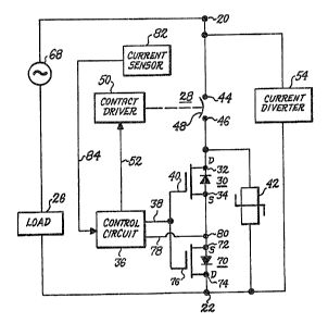
FIG. 7 illustrates an alternative embodiment for
diverting and interrupting a-c or d-c load current.
This embodiment lhas minimal power dissipation, i.e.,
substantially less than that of the embodiment of FIG.
5. It also does not require transformer coupling the
solid statsa devices of the controlled impedance circuit
as disclosed in 'the embodiment of FIG. 6. The a-c
source 68 and load 26 are serially connected across
terminals s;0 and 22 and the current diverter 54 is
connected across these terminals as in the embodiments
of FIGS. 5 and 6. Terminals 20 and 22 are connected to
the switch and controlled impedance network 92 via
lines 94 arid 96, respectively. Network 92 comprises
two parallel connected branches, each comprising a
switch and a conltrolled impedance circuit, i.e., MOSFET
device, andt a current sensor. The first branch,
connected between lines 94 and 96, comprises serially
connected first :witch 28 and first field effect
transistor 30. '.rhe second branch, also connected
between lines 94 and 96, comprises serially connected
second switch 98 and second field effect transistor
100. The dlrain and source electrodes of these two
transistorsc are reversed with respect to one another.
Drain 32 of the :first MOSFET 30 is connected to the
first switch 28 and its source 34 is connected to line
- 22 - 41PR-6470
96. Source 102 of the second MOSFET 100 is connected
to second switch 98 and its drain 104 is connected to
line 96. The bridging contact 48 of the first switch
is actuated by a first contact driver 50 and the
bridging contact 106 of the second switch 98 is
actuated by a second contact driver 108. A control
circuit 11o receives an input from current sensor 82
via line 112. It: has output lines 116, 118, 120 and
122 applied respectively to gate 40 of first MOSFET 30,
contact driver 50~, gate 114 of second MOSFET 100 and
contact driver 108. The control circuit also has a
common line 124 connected to line 96. A voltage
dependent device, e.g., varistor 126, is preferably
connected from th.e junction of the first MOSFET 30 and
the first switch 28 to the junction of the second
MOSFET 100 ,and the second switch 98. Device 126 thus
clamps the maximum potential obtainable across the
MOSFET devices.
Operation is described based on the assumption that
a-c load current initially flows through both parallel
branches. t3witches 28 and 98 are both closed. MOSFET
devices 30 and 100 are in full, i.e., saturation,
conduction because of a positive potential applied by
the control circuit, via lines 116 and 120, to the gate
electrodes ~~0 and 114 of both MOSFET devices 30 and
100. Devices 30 and 100 each have a minimal potential
drop, e.g., of the order of 0.01 volts. Under these
conditions, there is minimal power dissipation. The
total on re:aistance of the two devices 30 and 100
conducting :in parallel is only half that of a single
device and only one quarter of the on resistance of two
devices connected in series. Thus, the power
dissipation of the circuit of FIG. 7 is substantially
2~~~~~
- 23 - 41PR-6470
less, e.g., one quarter that of the circuit of FIG. 5.
However, the arrangement of FIG. 7 requires a more
complex control arrangement for the following reason.
In the previously described embodiments, current
diversion result:a merely from applying a zero or
- negative potential to the gate circuit of one or two
MOSFET devices so as to cut off the drain to source
conduction. However, in the circuit of FIG. 7, current
flows through two oppositely poled MOSFET devices 30
and 100 that are essentially connected in parallel.
Since these devi<:es have unsymmetrical blocking
characteristics, they can not be simultaneously cut off
in this manner. For example, assume that diversion is
commanded when the instantaneous polarity of the a-c
source is negative at terminal 20 and positive at
terminal 22 with current flowing from terminal 22 to
terminal 20. Ths: inherent junction diode of MOSFET 30
is then forward poled, i.e., poled in the direction of
current conduction. If the gate 40 of device 30 i's
then switched from a positive to a zero or negative
potential, device: 30 is not blocked, i.e., its current
flow is not cut off.
The following describes how current diversion and
interruption occurs. Current sensor 82 applies a
signal representative of the a-c load current via line
112 to control circuit 110. The control circuit thus
identifies when t:he a-c load current exceeds its
maximum allowable: magnitude and also the instantaneous
direction of current flow at such time. The control
circuit thereupon first switches the gate potential of
the MOSFET device: whose inherent diode junction is
forward poled at this time. Assuming that this occurs
when load current: flows from terminal 22 to terminal
- 24 - 41PR-6470
20, the inherent diode junction of MOSFET 30, but not
of MOSFET 1.00, i:~ forward poled. Accordingly, control
circuit 110 switches the potential on line 116, and
thus gate 40 of device 30, from a positive to a zero or
negative potential. Load current in device 30 now
flows through thEa inherent junction diode of the
device. Th.e potential drop across the device increases
to the potential drop across the inherent diode
junction which may be in the order of 0.8 volts. The
other MOSFET device 100 is still in full, i.e.,
saturation, conduction. It then has no inherent
junction diode and thus has a lower potential drop,
such as, for example, 0.01 volts. The potential drop
across device 30 is then substantially greater than
that across device 100. The voltage drop across the
first branch is therefore greater than that across the
second branch. Z'his causes the load current flowing
through the first: branch to transfer to the second
branch. Substantially all, or at least the major
portion, of the load current then flows through the
second branch. 'This major diversion results because
the percentage of load current diversion is inversely
related logarithmically to the ratio of the potential
drops across the respective MOSFET devices.
Upon transfer of load current from the first branch
to the second branch, control circuit 110 opens switch
28 of the first branch substantially under zero current
conditions. Specifically, it supplies a current pulse
on line 118 to contact driver 50 which thereupon opens
bridging contact 48.
Next, control circuit 110 turns off FET device loo.
Specifically, it switches the potential on line 120,
and thus on gate 114, from a positive to a zero or
a
- 25 - 41PR-6470
negative potential. Since the inherent junction diode
of device 1,00 is then reverse poled, this cuts off
conduction of device 100. (Device 126 limits the
potential across device 100 to a predetermined
allowable value.) This causes load current in the
- second branch to divert to current diverter 54.
Finally, upon load current diversion to diverter
54, control circuit 110 opens switch 98 under
substantially zero current conditions. Specifically, a
current pulse is supplied via line 122 to contact
driver 108.
FIG. 8 illustrates a simplified block diagram of
one embodiment of current sensor 82 and of control
circuit 110 including its output lines 116, 118, 120
and 122. This continuously detects the amplitude and
the direction of the load current. If load current
exceeds a predetermined maximum allowable value, the
control circuit supplies control signals necessary to
perform the above: described current transfer and
diversion o;perati.on. The control signals have a
predetermined sequence. First, the FET whose inherent
diode junction is~ then forward poled is gated off,
i.e., its gate potential is switched to a zero or
negative value, t.o transfer its load current to the
other parallel branch. Second, the switch associated
with that F:ET is opened in response to a current pulse
signal applied by the control circuit. Third, the FET
of the other branch is gated off to divert the load
current to 'the current diverter. Fourth, the switch
associated with this FET is opened in response to a
current pulae signal applied by the control circuit.
These operations must be performed not only in the
proper sequence, but also at appropriate intervals. In
- 26 - 41PR-6470
the embodiment of FIG. 8, these operations are
successively performed at predetermined time intervals.
The time occurrence of the current pulses that are
applied by the control circuit to the contact drivers
of the swii~ches must reflect the time that elapses
between them application of the current pulse and the
subsequent opening of the switch. Switches of the type
previously proposed by me; e.g., in U.S. Patent No.
4,644,309, issued February 17, 1987, open very rapidly.
They open within a few microseconds of the application
of the current pulse. Therefore, in this embodiment,
the current: pulse for opening a switch issues shortly
after its associated FET device is gated off. However,
in some cares it may be desirable to supply the current
pulse earl~.er. For example, the current pulse might be
applied simultaneously with the gating of the FET de-
vice. In Nome instances the current pulse may even be
applied bel:ore tlhe FET device is gated off, such as for
example whs:n utilizing slower switches. This applies
to the various eonbodiments, including those of FIGS.
5-7.
The spe:cific sequence in which the control signals
are issued depends upon the instantaneous direction of
the load current at the time diversion and interruption
is initiats:d. Specifically, it depends on which of the
two FET devices lzas its inherent diode forward biased
at the time:. If this is the FET of the first branch,
control signals are initially applied to that FET and
to the switch of the first branch and subsequently to
the FET and to the switch of the second branch. The
control circuit :110 of FIG. 8 includes a first chain of
devices to provide appropriately timed control signals
if the FET of the first branch has its inherent diode
forward poled. '.rhe control signals produced by this
- 27 - 41PR-6470
first chain sequentially control FET 3o and switch 28
of the first branch and subsequently FET 100 and switch
98 of the second branch. However, if the FET of the
second branch ha:a its inherent diode forward poled
during diversion and interruption, control signals are
first applied to the FET and to the switch of the
second branch and subsequently to the FET and switch of
the first branch.. The control circuit 110 of FIG. 8
therefore includsa a second chain of devices to provide
these control signals. These appropriately timed
signals of the second chain sequentially control FET
100 and switch 9Et of the second branch and subsequently
FET 30 and switch 98 of the first branch.
The embodiment is now described with reference to
FIG. 8. Current sensor 82 comprises a secondary
winding about load current line 94. This constitutes a
current transformer whose output is coupled via lines
112' and 112" to control circuit 110 shown by dashed
lines. The subsequently described components are all
within control circuit 110. Lines 112' and 112" are
connected in a first series loop comprising diode D1,
burden resistor 1.28 and diode D2. The diodes are poled
for unidirectional conduction such that load current
flow in the direcaion from terminal 22 to terminal 20
(FIG. 7) produces. a voltage across resistor 128. This
voltage thus appears whenever the inherent diode of FET
is forward poled. The output of resistor 128 is
applied to device: 130 via line 132. Device 130
provides any filtering of the half wave signal
30 necessary to remove spurious transients that otherwise
could improperly initiate current interruption. The
output of device 130 is applied to a first input 136 of
comparator.134. A source of d-c reference voltage,
- 28 - 41PR-6470
VREF. is applied to a second input 138 of the
comparator. The reference potential is adjusted to a
value equivalent to the maximum allowable value of load
current. :Cf the load current exceeds this maximum
value, i.e.., if the magnitude of the signal on first
- input 136 eaxceeds the reference potential on second
input 138, the comparator output 140 switches from a
first valuEa, e.g., a negative saturation limit, to a
second value, e.g., a positive saturation limit. This
transition initiates the control signals that transfer
load current from the first to the second branch,
divert load current to the current diverter and open
the switcheas.
The output 140 of the comparator is applied to
signal shaping circuit FET1. This provides an
appropriatsa quiescent output level, e.g., zero volts,
and~also a properly shaped trigger signal, e.g., a
positive pulse, :responsive to transition of the
comparator output. The output of circuit FET1 is .
supplied to one :input of first OR gate 142 and to the
input of time de:Lay circuit SW1. Responsive to a pulse
on at least: one of its inputs, the OR gate provides an
output pulse to pulse shaping circuit 144. The output
of circuit 144 is coupled via line 116 to gate 40 of
MOSFET 30 i.n the first branch. Circuit 144 normally
supplies a positive voltage to gate 40 to support
conduction of MOSFET 30. However, responsive to a
transition of th~a comparator output, its output is
switched to a zera or negative potential for a
sufficient time period to assure transfer of load
current from the first to the second branch. Time
delay circuit SW:L has a quiescent, e.g., zero level,
output, but: produces a pulse output at a predetermined
- 29 - 41PR-6470
time subsequent 1:o the occurrence of the pulse provided
to its input by t:he device FET1. The output pulse of
SW1 is supplied t:o one input of OR gate 146 and to time
delay device FET~~. OR gate 146, responsive to a pulse
applied to its input, provides an output pulse to
current pulse generator 148. Device 148 provides a
current pulse via line 118 to contact.driver 50 to open
switch 28 of the first branch circuit.
Time~delay device FET2 also has a quiescent, e.g.,
zero level, output and produces a pulse output at a
predetermined time subsequent to occurrence of the
pulse provided to its input by device SW1. The output
pulse of FE~T2 is supplied to one input of a third OR
gate 150 and to the input of device SW2. The
corresponding output of OR gate 150 is supplied to
pulse shaping circuit 152, which is of the same type as
pulse shaping circuit 144. The output of circuit 152,
connected via line 120 to gate 114 of MOSFET 100,
switches from a positive to a zero or negative
potential responsive to the output pulse of device
FET2. This diverts load current from the second branch
to current ciiverter 54.
Finally device SW2, which corresponds in type and
function to that of device SW1, provides a pulse output
to one inpuit of a fourth OR gate 154. The output pulse
of this OR gate, which occurs a predetermined time
subsequent ito the pulse applied to the input of device
SW2, is applied to pulse generator 156. Device 156
provides a current pulse via line 122 to contact driver
108 to open switch 98 in the second branch circuit.
The above described portion of the control circuit
provides control signals to divert and interrupt load
current responsive to overload currents sensed during
- 30 - 41PR-6470
intervals when a-c load current flows in a first
predetermined direction, i.e., from terminal 22 to
terminal 20. An additional equivalent arrangement
performs tYiis function during intervals when a-c load
current flows in the opposite direction, i.e., from
terminal 20 to 22. Control circuit input lines 112'
and 112" are connected in a second series loop
comprising diode D3, burden resistor 158 and diode D4.
These diodes are poled for unidirectional conduction
such that load current flow in the direction from
terminal 20 to terminal 22 produces a voltage across
resistor 158. Tlnis voltage thus appears whenever the
inherent diode o:E FET 100, in the second branch, is
forward poled. '.Che output of resistor 158 is applied
via filter device. 160 to a first input 164 of
comparator 162. Device 160 corresponds to and performs
the filtering functions of device 130. The d-c
reference potential, VREF, is applied to a second input
166 of comp~arator 162. If load current exceeds the
maximum allowablE: value of load current, the output of
comparator 162 switches in the manner previously
described. This transition initiates the control
signals that transfer load current from the second to
the first branch,, divert load current to the current
diverter and open the switches.
The output oi: comparator 162 is applied
sequentially to a second chain of device that
correspond to those of the first chain that was
previously descrp.bed. Thus, the comparator output is
connected to the input of pulse shaping circuit FET2A
that corresponds to circuit FET1. The output of FET2A
is connected in cascade to time delay devices SW2A,
FET1A and SW1A, respectively. Each of these
- 31 - 41PR-6470
corresponds to ita counterpart of the first chain,
i.e., SW2A to SW~~~, FET1A to FET2~, and SW1A to
SW2. The operat~.on of this second chain conforms to
that of the first: chain except for the sequence of the
control signals. The first chain produces control
signals for the ~:irst branch prior to those for the
second branch, in the sequence of FET1, SW1, FET2,
SW2. The second chain produces control signals for the
second branch prior to those of the first branch in the
sequence FET2A, ~'W2A. FET1A, SW1A. The outputs of the
devices in the second chain are supplied to second
inputs of the previously described OR gates to as to
avoid redundancy of the pulse shaping and pulse
generating circuits and of control lines. Thus, pulses
applied by eithez~ the first or the second chain will
generate the proper control signal. The outputs of the
devices of 'the second chain are of course connected to
inputs of t:he OR gates that initiate the appropriate
control signal. Specifically, device outputs are
connected to the second inputs of OR gates as follows:
FET2A to OR,gate 150: SW2A to OR gate 154; FET1A to OR
gate 142; and SW1A to OR gate 146.
It should be apparent to those skilled in the art
that while .embodiments have been described in
accordance with the Patent Statutes, changes may be
made in the disclosed embodiments without actually
departing from the true spirit and scope of the
invention. For example, the embodiments disclosed
herein may utilize parallel connected transistors and
sets of separable contacts to accommodate higher
currents and to permit the use of plural separable
contact structures. Specifically, they may utilize a
- 32 - 41PR-6470
plurality of parallel connected semiconductor devices
instead of a single device, plural sets of parallel
connected :~eparalble contacts instead of a single set of
separable contacts, or parallel arrays of separable
contacts and semiconductor devices instead of a single
set of separable contacts and a single semiconductor
device.