Note: Descriptions are shown in the official language in which they were submitted.
41Q 9t/0766° PCT, /L ~40/06~~ z
F LUIDICS EIAi7 FOR 'i'ES ~'~';C
Ci:EMICAL A2:D IOi:IC SL::S:,RS
FIEr..D OF TFiE T_N~.'F.::.0;:
This invention relates to a:;bie.~.t .sensing de~~:.oes
such as ion sensitive and chemically sensitive devices a::~ :.~
methods of testing such devices in appropriate environme.~..s.
BACKGROUND OF THE INVENTION
It frequently is desirable to :nonitor the
composition of the chemical environment, for example, to
regulate ohemical or biochemical processes, to determine a~.r
or water quality, or to measure parameters of interest i~.
biomedical, agricultural or animal husbandry disciplines.
Because of the nature of the cher"ical environ:~e.~.~,
it is desirable that any measurement apparatus have at leas:.
some of the properties of: low cost, simple fabrication
methodology, digital operation, some degree of signal
preconditioning or intelligence, small sire, high chemical
sensitivity with selectivity, multiple species infor:,iation
with specificity, choice of reversible or integrating response
20 to chemical species, temperature insensitivity or dompensation
and low power requirement. Ln addition, the measure".ent
apparatus should have good long to m electrochemical
stability, good physical resiliency and strength and goo:
resistance to corrosion and chemical attack. In the case of
25 electrical measurement devices, the devices should also have
low electrical impedance to provide good signal to noise
ratios. With chemically sensitive devices, the devices should,
also have a Hernstian response to the chemical phenomena being
measured.
30 One method for the detection, measurement and
monitoring of the chemical properties of. a substance involves
the measurement of an electric potential where the potential
is dependent upon the chemical activity being measured.
Bergveld has proposed that hydrogen and sodium ion activities
~~O 91/0766,' P CT/L S90/06~_3
in an aqueous solution be measured by a :;fetal oxice
semiconductor field-effect transistor (t~iCSFET) ~~~'_«e~
removal of the gate metal. P. Bergveld, '°Developae~:~,
Operation, and Application of the Ion-Sensitive Field-E_°eot
Transistor as a Tool for Electrophysiology" IEEE Trar.saot_c::s
of Biomedical Enqineerinc~, Vol. BME-19, pages 342-35~
(September, 172). In particular, if a MOSFET with no gate
metal were glaced in an aqueous solution, Bergveld sugg=_s~e
that the silicon dioxide insulation layer would become
hydrated and then, because of impurities in the hydrat a
layer, ion selective. After hydration o.f the insulation layer
o.f the MOSFET, Bergveld believed the device could be used for
ion activity measurement by immersing the device in the
solution in question and then recording canductivity changes
of the device. Thus, the Bergveld device is commonly referred
to as an ion-sensitive field effect transistor (ISF~T).
Bergveld's work led to other developments in the
field of ion sensitive electrodes such as the chemical
sensitive field effect transistor (CHEMFET) device described
in U.S. Patent 4,020,30. As described in the '230 patent,
the CHEMFET is a MOSFET in which the gate metal has been
replaced by a chemically sensitive system that is adapted to
interact with certain substances to which the system is
exposed. Thus as shown in Fags. 1 and 2 of the '830 patent,
the CHEMFET is identical in structure to a MOSFET except for a
sensing layer or membrane 3$ that is deposited in place of a
metal gate layer on the oxide insulator above the channel
region of the transistor and, optionally, an impervious layer
4~ that covers all other parts of the CHEMFET that might be
exposed to the solution. Numerous variations on CHEMFc..T
structures are disclosed, for example, in U.S. Patents
CA 02068213 2001-11-09
- 3 -
4,180,771, 4,218,298, 4,232,326, 4,2..38,757, 4,305,802,
4,332,658, 4,354,3()8, 4,485,274, 4,:397,714, 4,739,380 and
5,200,051.
The concept of an ISFET or CHEMFET is especially
attractive because of the promise ii:. holds that the high volume,
low cost fabrication techniques that= are used to manufacture
field effect transistors (FETs) in i_nt.egrated circuits may
somehow be adapted for ~:he manufacture of ISFETs and CHEMFETs.
Advances in such technology are disclosed, for example, in the
above-referenced U.S. Pat:e~nt 4,739,380 and U.S. Patent No.
5,200,051.
One problem encountered in the fabrication of
integrated circuits (ICs) is the testing of such devices.
Because integrated circuits are so small and yet so complicated,
testing imposes major problems in the handling of ICs and in the
design of appropriate te:~.ting devices and protocols. At the
same time, testing is needed as a process control to ensure that
the IC manufacturing process is operating as desired and to
identify the inevitable ruumber of ICs that do not meet
specifications for whate~~er reason. Testing is a particular
problem in the manufacture of ISFETs and CHEMFETs since these
devices are transducers which convert environmental variables to
an electrical signal. ';omplete testing of such devices requires
that the testing be carried out by exposing the ion sensing or
chemical sensing layer o:f- these devices to the environment which
the ISFETs and CHEMFETs acre designed t=o measure. One manner of
testing is disclosed in x_1.5. Patent 4,864,229.
A critical component of the testing of integrated
circuits is the fluidics head which contains the test fluid
which the ISFETs and CHEI~IFETs are designed to measure. The
fluidics head must provide leakproof engagement with the sensing
electronic circuit devicE>. to be tested so that
~'O 91/0i66' PCT/C S90/06=?Z
_ ,~ _
neig:~.boring devices on the wale= are not conta~inat=~ W.~ ..:~:e
test fluid. Additionally, because small volu:~es o~ test
fluids (on the order of 20-100 ~1) need to be handled and
because of the small size of the devices, great care ~~.:st :,e
used to avoid entrapment of air bubbles and fluid
contamination during the testing of the devices and upon
changing from one test fluid to another. The fluidics head
must be designed to test devices lying on a variety of planar
wafer materials. These materials include alumina, high
melting plastics, glass, silicon, silicon dioxide and si'_ico:~
nitride.
SL':~I:MARY OF THE INVENTION
It is an object of the present invention to provide
a fluidics head which is capable of rapid leakproof engagement
and rapid breaking of leakproof engagement with a planar wafer
surface thereby facilitating rapid testing of sensing
electronic circuit devices lying on the planar wafer surface.
0 It is another object of the present invention to
provide a fluidics head which is structurally strong and
capable of providing leakproof engagement with the sensing
electronic circuit device over a wide range of fluid flow
rates.
Another object is to provide a fluidics head which
permits the exposure of one or more sensing electronic circuit
devices to one or more test fluids without significant
entrapment of air bubbles or test fluid contamination.
These and other objects of the invention as well as
the advantages are the subject of the following detailed
description and claims.
The foregoing objects are achieved according to the
present invention by means of a fluidics head for
automatically testing chemical and ionic sensing electronic
W't791/Oi66" ~ PCT/Cj90106~~Z
circuit devices comprising (a) a fluid confining cell hav.~.r,
<1.~:.,
at least one open orifice to contain a known test _ _.., ..,
means for filling a test fluid into said open orifice a:~~
discharging the test fluid from the open orifice when 4he cel'_
is in leakproof engagement with a sensing electronic circui°.
device to be tested, and (c) means for providing elec:.~'_cai
contacts to the sensing electronic circuit device so as to
test the sensing electronic circuit device with the test
fluid. Such a means for providing electrical contacts, for
example, may be obtained by use of spring loaded probes
contacting the electrical leads of the integrated circuit of
the sensing electronic circuit device.
Typically, the means for filling and discharging the
Z5 test fluid from the open orifice comprises one inlet opening
and one outlet opening in the fluid confining cell.
Preferably, the inlet opening and the outlet opening are at .
opposite ends of the fluid confining cell. The open on °ice
which is connected to the inlet and outlet openings has a.n
20 internal shape which minimizes the entrapment of air or
residual test fluid upon filling the fluid confining cell wit:
a test fluid and upon discharging the test fluid from the
fluid confining cell. Preferably, the internal shape is such
that the open orifice is shaped at its ends to closely confor,:~
25 to the shape of the inlet and outlet openings. Most
preferably, the internal shape comprises ends approximating
half sections of paraboloids with no angled corners se as to
permit the maximum degree of laminar flow and thus minimize
non-lamimar flow of the test fluid through the fluid confining
30 cell. Generally, all angles should be as obtuse as is
feasible with a single molded piece.
Another possible manner of contaminating the test
fluid is the depletion of species dur~.ng the testing of the
sensing electronic circuit devices. This is evident in
w o 9 no~ss-
Pcries9oia6~~z
-6-
sensing electronic circuit devices principally relyi::g c:-.
amperometric methods in which the bulk concentration o_
electroactive species is changed by the oxidation o~ :ed::c~~c-.
reactions occurring at the electrode solutian interface. '=':~~s
is especially evident when small volumes of test fluids are
used. Thus, in order to accommodate such changes in
concentration, the internal volume of the fluid confining cel:
having an open orifice must be sufficient to per-iit buff:
solution characteristics to prevail. Preferably, the volu;,~e
of test solution must be sufficient to preclude any
significant change in electroactive species concentration,
i.e., less than or about 1% during the period of test.
The design of the fluid confining cell is such that
when a vertical force is applied to the cell when in contact
with a planar surface, the force vectors are predominantly
compressive, thus minimizing lateral stress and obviating
buckling. The fluid confining cell design is also optimized
for the desired fluid dynamics based on observations of actual
fluid flow as well as precision arid accuracy measuremen~a of
the chemical and ionic sensing electronic circuit devices.
The design is particularly directed towards high flow ra=es oz
fluids, where potential leakage problems are more pronounced.
Particularly, the invention provides for a fluid confining
cell having a supportive structure of sufficient strength to
permit leakproof engagement with the sensing electronic
circuit to be tested when the open orifice of the fluid
containing cell is urged onto the circuit. Preferably, the
supportive structure is wedge- like in shape with rounded outer
edges. The rounded outer edges conforn, to the planar wafer
surface on which the circuit is fabricated so as to form a
leakproaf seal.
ti'p 9 i /07b6-
PCT/L S90/06~~?
_;_
The fluid confining cell is typicall;~ ~;,oide~ -o "a
desired shape. The material used for the ce'_:. .-"us:. sags°;'
several recuirements. Among these requirements aye (yy
chemical inertness to the fluids used; (2) no adsorption o~
chemicals: (3) physical strength to provide controlled
deformation and sealing, but to resist buckling when :.r.ged
against a circuit to be tested and during fluid flow; and (~;
ability to provide air and fluid seal.
BRIE: DESCRIPTTON OF T:~S DRA'rvi:;GS
The above-described features and advantages o° the
invention will be more readily apparent from the Following
detailed description of the preferred embodiments of the
invention, which is provided by way of illustration, and the
appended figures in which:
Figure 1(a) and 1(c) illustrate the fluid flow
effects when fluid initially enters the orifice of the .fluid
confining cell. To avoid the formation of recirculation zones
at section 1(b), angled corners of the orifice are eliminated
and the inlet opening is gradually increased in diameter as is
illustrated in Figure 1(c).
Figure 2 illustrates an overview of a wafer
comprising a plurality of sensing electronic circuit devices
with an expanded view of one such device. The area (3)
defines the lacation where the fluid confining cel.1
establishes a leakproof engagement with the sensing electronic
circuit devices (1).
Figure 3 shows a bottom view of one embodiment of
the fluid confining cell.
~"igures 4(a) and 4(b) show crass sectional views of
two embodiments of the fluid confining cell.
~'O 91/0766." ~ ~ ~ ~ ~ PCT/L'S90/065'3
_8..
F figures 5 (a) , 5 (b) and S (c) depict several ~,~ie~.;s o~
a less preferred fluid confining cell having square come=s.
The corners (1) are potential entrapment/turbulent a:eas.
Figure 6(a) to (d) show several views of one
embodiment of the frame which supports the fluid confinin?
cell and spring loaded probes for fluitlic and electrical
contact with the sending electronic circuit device.
Figure 7 is one embodiment of the testing appara:.us
having a multiplicity of fluidics heads for the simultaneous
testing of a multiplicity of sensing electronic circuit
devices on a wafer.
Figure 8(a) arid (b) is a flow chart of the tes-~ing
process ezsploying the fluidics head of the invention.
DETAILED DESCF2TP'rION OF THE INVENTIOid
Figure 1(a) shows the separation of fluid flow at
thA edge of the orifice of the fluid confining cell just
beyond the inlet opening. The main fluid flow maintains the
original velocity immediately through the opening to form a
commonly termed vena contracta at Section 1(b) of Figure 1(a).
The main fluid flow then decelerates to fill the orifice.
This causes recirculation zones to form at the corners o: the
orifice which results in increased mixing, and trapping of
suspended particles, fluid and air bubbles. Such adverse
effects are substantially reduced by gradually increasing the
diameter of the inlet opening. Therefore, the preferred
embodiment of the fluid confining cell has an orifice with
walls shaped as shown in Figure 1(c) approximating the S-curve
of two intersecting parabolas.
Figure 2 depicts sensing electronic circuit devices
having integrated circuit chips (1) which are physically
offset from their electrical leads (2). The area (3) defines
the seal formed when the outer edge of the fluid confining
W O 91 /0 %~b6' ~ ~ ~ ~ per'; l ~90/Ofi1'3
_g_
cell is urged onto the plane (4) of the integ:ated circuit
chip. As shown the fluidics head containing the fluid
con°ining cell can be advantageously used in testi;;g an
extended gate field effect transistor (EGFwT) such as that
disclosed in the above-referenced LT. S. Patent 4,739,380.
Figure 3 degicts the bottom view of the fluid
confining cell (1). The inlet (2) and outlet (3) openings in
which test fluid enters and discharges are located at opposite
0 ends of the open orifice (4). The open orifice (4) of the
cell closely conforms to the circumference of the inlet and
outlet openings so as to permit the maximum degree of laminar
flow of the test fluid within the cell.
The material used to fabricate the fluid confining
cell must be chemically inert, unable to adsorb chemicals, of
sufficient physical strength and able to provide air and fluid
seal. Room-temperature Vulcanized materials (RTV) and
silicone-based materials such as Silasti.c", an organo-
polysiloxane elastomer, made by Dow have been found to be
especially useful in satisfying these requirements.
zt is feasible that the fluid confining cell (1) may
be comprised of more than one piece i.e. a solid fluid
confining cell (1) with an inserted o-ring along the outer
edge of the open orifice (4). However, such a design has
several drawbacks. Compression of the o-ring leads to the
formation of acute angles within the structure which promote
the entrapment of air and other contaminants. Additionally,
the number of interfaces is increased with concom-ittant
increase in the number of potential leakage paths. Finally,
the geometry of an o-ring limits the range of possible sealing
designs of the fluidics head.
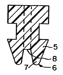
Figure 4(a) depicts the cross sectional view of the
fluid confining cell. The supportive structure (5) is wedge-
like in shape with raunded outer edges (6) so as to provide
~'O 91/Oi66~
PCT/L S90/06~2?
. _yp~
leakproof engage:,~ent with the sensing integrated cirw.;'_:. c..
when the cell is urged onto the plane of the integrated
circuit chip. The acute angle made by the two sides o~ t::e
supportive structure (7) is preferably more than l0 decrees.
The radius of the rounded outer edge (6) is preferably 0.25 c~
the maximum internal width of the fluid confining cell. :he
tog (8) of the fluid confining cell as shown is flat, as sup::
a contour practically can be easily milled. However, the
1p preferred contour is concave as shown in Figure 4(b) which
would permit the maximum degree of laminar flow.
Figures 5(a) to (c) depict another less prefer=ed
embodiment of the fluid confining cell having square corners.
Figure 5(b) is a top view and Figure 5(c) i.s a side elevatio"
view. The areas near these square corners (l) present
potential problems of air entrapment and contamination from
residual test fluids due to recirculating flow. Such proble:~s
of mixing result in lower precision and accuracy in the
measurement of the chemical and ionic sensing electronic
circuit devices such as those described in Figure 2. Such
problems are especially noticeable where an individual sensing
electronic circuit device is exposed to several test fluids in
succession, thereby requiring a change of test fluids in the
fluid confining cell.
Figures 6(a) to (d) depict several views of the
frame which supports the fluid confining cell and spring
loaded probes for fluidic and electrical contact with the
sensing electronic circuit device. Figure 6(b) is a plan view
of the top. Figure 6(c) is a front elevation. Figure 6(d) is
an end elevation. The fluid confining cell is secured by
sliding along track Z to the center of the frame. The
passages 2 hold a multiplicity of spring loaded probes. The
passages 3 hold the tubing which is connected to the inlet and
outlet openings of the fluid confining cell. The bores 4
tt'O 91/07b6' PC'f/l ~90/06~=3
-11-
allow the frame to be secured to an a'_ign~e;~~ apparawus
allows screw adjustments of the leveling of the f=uid
confining cell with respect to the planar wafer surface.
alignment apparatus automatically selects and positions ir.
succession a multiplicity of sensing electranic circuit
devices on a planar wafer surface for leal~:proof engagement
with the fluid confining cell.
Figure 7 illustrates one embodiment of the t estir.;
apparatus in which the frame 1 holds a multiplicity of fluid
confining cells 2 along with their corresponding spring loaded
probes 3. As shown, the fluid confining cells are urged
against the surface of the wafer 4. The spacings of the fluid
confining cells are such that these cells are urg e' into
leakproof engagement with a multiplicity of sensing electronic
circuit devices thus allowing these devices to be tested
simultaneously.
The circuit devices 3 on the wafer 4 are aligned
into position with respect to the fluid confining cells by an
x,y and theta positioning table 5 which holds the wafer fro.~,.
below.
Figure 8 outlines the flow chart used in testing a
plurality of sensing electronic circuit devices employing the
fluidics head of the present invention. The cha r
particularly shows that each device is tested with two
solutions, although any number of solutions may be used.
The apparatus disclosed can be implemented or
engineered in a number of ways. The description is intended
to illustrate the principles and mode of operation of the
fluidics head and not to rigidly define the structure or
process. It is understood that changes and variations can be
made therein without departing from the scope of the invention
as defined in the following claims.