Note: Descriptions are shown in the official language in which they were submitted.
2068415
CAPACITIVE POWER SUPPLY HAVING
CHARGE EQUALIZATION CIRCUIT
RAC~ OU~d of the Invention
The present invention relates generally to capacitive
power supplies, and, more particularly to a capacitive power
supply having a charge equalization circuit which ensures
that the electrical charge cQl1ected and stored by the capacitive
power supply does not eYcee-l a pre-determined level.
In order to ~er .~, operation of an electrical device at a
loc- t;or not prUyim~ts to a perm~nent power source, a
portable power supply is positioned proYimAAts to the electrical
device. Once the portable power supply and the electrical
device are suitably cQnnecte~l theretogether, the portable power
supply _ay be ~ 7e~l to power the electrical device thereby.
Conv.snt;QnAlly, a portable power supply is formed of an
el6cho~hemical material, and energy is stored by the
ele~lloch~mic~1 material in the form of chemical energy.
Power required to operate the electrical device is fo~ ~ed by
cvL~verLing the stored, chemical energy of the electrorhemical
_aterial into electrical energy.
Such a conventional, electrochemicA1 power supply is
commonly referred to as a battery, and one or more
commercially-avAilAble batteries may be utilized to generate a
direct current voltage to power many varied types,
constructions, and ~lesign~ of electrical devices. Such
-1- ~
2068~I5
conventional, electrorhPmical battery power supplies are
widely av~ hle, and, thelefo~e, are ~lvelliently utilized to
form the portable power supply to power an electrical device
thereby.
A c.,~v~.. tion~l, electrorhemir~l battery is, however, of a
finite ene,gy storage capacity. Thelefole, a single battery (or
several batteries cQnn~cte~l theretogether) may be utilized to
power an electrical device for only a limited period of time. As
the stored, che~nic~l energy of the electrorh-mic~l material is
; 10 converted into electrical energy to power the electrical device,
the battery beCQmê~ ch~rged a~ the stored ch~mir~l energy
CQ t~incd by the elec~roc~ nic~l material bec~me~ dissipated.
Once the rçm~inir~g, stored energy of the battery is
depleted below a cel laill level, repl~cçmçnt of the battery is
15 npce~sitated to yermit CQnt;nlletl operation of the electrical
device. The frequency with which the battery must be
repl~ce-l, is, of co~rse rlepçn~lpnt upon the battery capacity
(i.e., the amount of energy stored in the battery), the energy
l~q,liled to operate the electrical device, and the frequency
20 with which the electrical device is operated. Other types of
portable power supplie~ are ~imil:~rly of a finite energy storage
capacity, and, the~efole, ~imil~rly bec~ms depleted of stored
energy after a period of use thereof.
A battery-type construction ~myl;sed of a nickel-
25 cad~ium (Ni-Cd) material is often utilized to power an
electrical device. The use of the nickel-cad_ium material to
form the ele-l~k^-nir-~l material is advantageous for the
reason that, once a battery formed theref~olu is depleted of
stored energy, an electrical, charging cumnt may be applied
30 to the battery to recharge the battery thereby. Battery-type
constrllcti~n~ com~l;sed of other materials may ~imil~rly be
recharged once depleted of stored energy by the applic~t;o~ of a
charging current thereto.
2068415
Battery-type constructions comprised of a nickel-
ca~iul.l material (as well as other such ~imilsr materials)
are not of unlimited battery-lifes. That i8 to say, a
rechargeable battery comprised of such a material cannot be
S recharged and reused an llnlimited numher of times. Over
time, as the nickel-cad~iu~ battery is tli~h~rged, and
s~lhse~uently recharged, the efficiency of energy col,valsion of
electrical energy (supplied by the charging current to recharge
the battery) into stored ch^~;~-s-l energy of the ele_llo&~ nic~l
10 material is re~ ce~l Over time, such reduction in effi~içncy of
energy conversion mPlres impr-s-ct;c-s-l cor ~;nne~ reuse of the
same batbry. Once the battery may no longer be çffi~iently
recharged, the battery must be discarded and replece~ with a
battery ~qp~ble of being çffi~iently recharged to permit
15 cent;n~le~ powering of the electrical device.
Additionally, when recharging a rechargeable battery,
the rate at which the charging current is ~p~lie~l to the battery
must be controlled. If the charging current applied to the
battery to recharge the battery thereby is beyond a certain level,
20 the battery may be tl~m-s~ged by the charging current. The
msYimllm, allowable level of charging current which may be
applied to various ba~te~ type constrl~1;or ~ to recharge the
battery thereby varies. For inqtsn~e~ a rechargeable battery
~ ;sed of the aforementioned nickel-cadmium material
25 may be recharged with a charging current of 600
mill~mpereg. A ba~Le, ~-type construction cv~ ;sed of a
lithium material (another material of which a rechargeable
ball~l~, may be com~r;sed)~ ccnve~3ely, r-s-nnot be charged with
a charging current in excess of 100 milli~n~ele8. Battery
30 charging apparatus utilized to provide the rechargeable
battery with the charging current to charge to the battery
thereby cannot be llt;li7e-1 to recharge rechargeable batteries of
the various battery-type constructions without al ~ro~l;ate
alteration of the level of the charging current.
2068~15
Further, because the level of the charging current
applied to t_e rechargeable battery c~nnot P-c~e~l a certain,
m~Yimum level, the charging rate of the battery cannot be
increased beyond the allowable level, and the time required to
5 recharge a baLt~ ~, once tliRrh~rged to a certain level, cannot
be reduced below a cel lai~ n time period. If only one
rec_argeable battery i8 av~ ble to power the electrical device,
the electrical device c~nnot be operated once the battery has
been li~h~rged h~nq~t~l a ...;..i.n~ level, and the time
; 10 period required to recharge the battery to a level above the
u~ level to permit cQnt;nlle~l operation of the load
~,lçm~n~, c~nnot be reduced less than the. minimllm time
period.
Still further, when charging a rechargeable battery,
15 such as a nickel-cadmium battery, with a m~imum,
allowable charging current, once the battery l~ecQ~ne~R fully
charged, applic~tio~ of the charging current at the high
charging level to the battery must be termin~te~l Continlled
charging of the battery at the high charging rate can cause
20 gPQ~Q~;ng~ electrolytic venting of the battery, perm~npnt 1088 of
balle~ capacity, and physical ~l~m~e to the battery.
Other constr~lctiQnQ- of portable power sou~es are
known, but heretofore have been pr~ctic~l for only low power
aprlic~tionQ In particular, capacitive power sources have
25 been lltili7e~l as back-up power supplies for integrated circuit
m^mories to power the integrated circuits for short periods of
time, such as may occur during temporary power
inte~ ~ ulJ~ions.
C~r~citors having capacitances of values great enough
30 to generate current levels to power most electrical devices
(e.g., a consumer electronic device such as a portable
radiotelephone) for eYt~n~le~l periods of time have previously
been impr~ctir~l for the reason that the capacitors forming
such capacitive power supplies would be of prohibitively large
2068415
~im~cion8. Other of such capacitive power sources are of
very high effective resist~nre~, and are 8im~ rly impractical
for u~e to ~enerate lar~e current levels. However, U.S.
Patent No. 5,187,640 issued February 16, 1993, and
5 entitled "C~p~tive Power Supply" by Metroka et al. disclose~
a capacitive power supply c~p~ble of generating signifi~ ~nt
current levels for an e~tende~ period of time.
The capacitive power supply t~ loEe 1 therein is capable
of generating a continuous current level in escess of 600
10 milli~mperes for a time period in escess of one and one half
hours. Once the charge stored by the capacitive power supply
ha8 been depleted through tli.sch~rge of t~e stored energy of the
supply, the capacitive power supply may be quickly recharged
by application of a charging current thereto.
When several of the capacitive elements forming the
capacitive power supply are connecte-l in series, any variance
in the capacitive values of the capacitive elements results in
unequal amounts of charge being stored by various ones of the
capacitive elements when a charging current is applied
20 thereto. Termination of application ofthe charging current
once a first of the capacitive elements becomes fully charged
l,le~ellts all of the capacitive element~ from being fully
charged. Conversely, continued application of the charging
current to the circuit after the first of the capacitive elPments
25 has been fully charged is inefficient, and could result in
arcing of charge across plates of the capacitive elements, or
even perm~npnt ~m~ge to the capacitive elements..
What is needed, therefore, is a capacitive power supply
which may be efficiently charged to a pre-determined level.
'~.
20684 1
-6-
SllmmD~ry of the Invention
It is, accolLllgly, an object of the present invention to
provide a capacitive power supply c~p~h1e of generating a
5 pote ti~l difference of a precise, known value.
It is a further object of the l"c~e..t invention to provide a
charge eq~ t;~n circuit for a capacitive power supply.
It is a yet a further ob~ect of the preae.lt invention to
provide a capacitive power supply for ~.. ~ g a portable
10 transceiver, such as a radiotelephone.
It is a still a further object of the present invention to
provide a raAiotelephone construction 1'~ e~ed by a capacitive
power supply.
In accordance with the present invPntion, thelefore, a
15 portable, rechargeable power supply foll.li,~g a power source
of pre-~lefine l characteristics for ~. el;ng a load elempnt
when coupled thereto i9 disclosed. The power supply has a
first conductive surface comprised of a conductive material for
cQ11ecting and storing electrical charge respQn~ive to
20 application of a charging current thereto. A gPcQntl
conductive surface is co l,l;sed of a conductive material, and
is sp~ce~l-apart from the first con~llJctive surface whereby a
potential difference is formed bel~. ee~l the first co~ tive
surface and the secQn-l conductive surface when electrical
25 charge is stored upon the first conductive surface. The first
cr~n~lllrtive surface and the second conductive surface are
together of a low electrical resistance to minimi7e, thereby,
resistive loss across the first and secon~l conductive surfaces
during ~ rh~rge of the electrical charge stored upon the first
30 conductive surface to power the load elem~nt when couplet
thereto. Once the potential difference formed between the first
conductive surface and the second conductive surface is
beyond a pre-determined value, the level of the charging
current applied to the first conductive surface is reduced.
~7~ 2068~1~
Brief Description of the Drawings
The present invention will be better understood when
5 read in light of ^ccomr~nying drawings in which:
FIG. 1 i8 a circuit schem-s-tic of an actual capacitive
elrment having intrinsic series and parallel resistances
^~Eocis-te~ therewith;
FIG. 2 is a circuit sçhem-t;c of plurality of ideal
10 capacitive elçm^-^t~ c.^,nnected in a series connection
therebetween;
FIG. 3 is a circuit sçh^m-tiç~ 8imi19r to that of FIG. 2,
but illustrating a plurality of actual capacitive elçmçnt~
hPving e~clive series resi~t~nres ~sori~te~l therewith and
15 c~An~Act~d in a series conn?ct;~An therebetween;
FIG. 4 is a partial circuit srh~m-s-t;c~ partial block
diagra n of the rechargeable power supply of the present
invention;
FIG. 5 is a gr~phir-s-1 represent-s-t;Qn of the
20 characteristic curve of a conveti~ns1 diode;
FIGs. 6A and 6B are circuit sçhPmst;çR similAr to that
of FIG. 4, but illustrating first and secQnd circuit
imrlem^ntstionR of the shunt circuit of the rechargeable
power supply of the present invent;Qn;
FIGs. 7A and 7B are circuit srhem-s-t;r~ simi1sr to that
of FIG. 4, but illustrating third and fourth circuit
implem~nt-stiQrl~ of the shunt circuit of the rechargeable
power supply of the present invent;on;
FIG. 8 is a circuit ~chPmAtic of a circuit ~imil~r to that
of FIG. 6A, but wherein a plurality of capacitor-shunt circuit
pairs are st~çke-l theretogether in a series cQnnection;
FIG. 9 is a circuit 8çh~m~tic~ 8imils~r to that of FIG. 4,
but illustrating a fifth circuit implemrnt~tion of the
rechargeable power supply of the present invention;
2068~ t 5
-- -8 -
FIG. 10 i8 a circuit s~hem~tic of a circuit ~imilAr to that
of FIG. 9, but wherein à plurality of capacitor-shunt circuit
pairs are 9~ ^lre~3 theretogether in a series co~nection;
FIG. 11 is a circuit srhem~t;c of an alternate
5 ~mhoAimo~t of the rechargeable power supply FIG. 10;
FIG. 12 is a partial circuit scho!m~t;c, partial block
diagram of the rechargeable power supply of the present
invention cQnnect~l to power a load ~lem^ ~t thereby;
FIG. 13 is a block diagra_ of a transce;ve~ which _ay
10 be powered by the capacitive power supply of the present
invention; and
FIG. 14 is a cut-away, schem~tic view of a portion of the
capacitive power supply of the present invent;on
Description of a P~efer~ed ~.mho~limant
Referring first to the circuit schem~t;c of FIG. 1, a
capacitive element, ~eferfed to generally by .efe~e.lce numeral
10 is shown. Capacitive element 10 is co~ r;sed of first plate
20 mPmher 14 co~ ;sed of a conductive material having a
surface formed thereupon. Spaced-apart from plate memher
14 is plate memher 18 which is ~imil~rly C6 l,~;sed of a
cQn~llctive material having a surface formed thele~l,or~ Lead
22 is electrically coupled to plate m~-nher 14; ~imil~qrly, lead 26
25 is electrically coupled to plate memher 18. Preferably, leads 22
and 26 are integrally formed with their ~e~l,e~ ;ve plate
members 14 and 18 and are c6~ r;sed of the same materials
as those of plate memhers 14 and 18, respectively.
Plate memher 18 is spaced-apart from plate m~mber 14
30 by a length indicated by arrow 30. A gaseous material, such
as air, having a constant dielectrical value may be positioned
in the gap separating plate memhers 14 and 18. Altemately,
and as illustrated, other mate~als, indicated by material 32,
having other dielectrical values may be positioned between the
35 gaps separating the plate members 14 and 18.
-8-
2068~1 5
-- g
Further illustrated in FIG. 1, in hatch, are resistors 34
and 38. Re~;~tor 34 is represAntql~;ve of an e~cLive series
re~ nce intrinsically ~so~te~l with an actual capacitive
çlçmDnt Re~;~t~r 38 is ro~e~n~t;ve of the shunt resistance
5 between the sp~re-l-apart surfaces formed upon plate
members 14 and 18. The resistive value of resistor 38 is also
indicative of le~l~e between the surfaces formed upon the
~h~g plate mçmber8~ PQC~ e the shunt re~iP~qn~e, here
le~.escnted by resistor 38, is typically of a very large value,
- 10 resistor 38, for prrctj~ ~l purposes, forms an open circuit, and
need not be cQn~ Dred further. Ho~ e~er~ the effective series
resistance, here relJ,e~ents~ by resistor 34, although of a low
value, may be of significance, especially when several
capacitive elDmDnts 10 are connDcts~l in a series connection.
15 When connects~ in such a parallel connact;Qn, the e~eclive
series re~i~t~nre of each of the capacitive Plçm^nt~ may be
~llmme-l, and the magnitude of the equivalent resistance
formed the~ef~o~ is a multiple (if the series re~i~t~nces of
each of the capacitive Dlem~Dnts are of equal values) of the
20 effective series re~i~t~nc~Ds of each of the capacitive elemDntg
10.
Connçct;on of a charging current source across
opposing plate mDmhers 14 and 18 of capacitive element 10,
such as, for Dy~mple~ by connection of opposite sides of the
25 charging current source to leads 22 and 26, c~ es electrical
charge to be for_ed upon one of the plates. rosilive charge
indicators 42, illustrated in FIG. 1 proYim~te to plate 14, are
indicative of such electrical charge formed upon plate member
14. To form a positive charge upon the surface of plate
30 mPmher 14, a positive side of the charging current source is
connecte-l to plate memher 14, and a negative side of the
charging current source is coupled to plate 18. The electrical
charge formed upon one of the plate mpmbers rem~in~ even
after the charging current source is ~ connçcte~l from the
-lO- 2068415
plate memhers 14 and 18. Electrical charge formed, and
thereafter stored, upon one of the plate members of the
capacitive element 10 causes capacitive element 10 to function
as a charge (i.e., energy) storage device. The potential
5 difference formed across the sp~ce~l-apart plate members 14
and 18 permits the capacitive elçm~nt 10 to function as a power
supply to power a load ~lement when the opposing plate
m^mhers of the capacitive elemPnt 10 are suitably coupled
- across a load elem~n~.
It is to be noted that capacitors of other tlesi~n~ may be
constructed to have spaced-apart surfaces formed upon
structures other than plate mçmbers~ but which 8imilPrly
function as charge storage devices.
Previously, capacitor const~-~ion~ which were of large
15 cspacitive values were of significant physical size. Capacitor
~le~ignR are now known, however, which are of both high
cspacitive values and also of small physicsl limen~ions. For
ç,~mple, the capacitive po ver supply tisclosed in the
afore..,e ~lioned U.S. Patent No. 5,187,640 issued
20 February 16, 1993, is comprised of capacitive
elçmçnts having sp~ce~l-apart plates, each of which are of
aress of ay~,o~mately 40 square centimeters and 5 mils in
depth, snd which are of capacitances of approximately 6000
farads and capable of forming a potential difference between
25 opposing plate m~mbers of 1.2 volts. The plates of the
capscitor sre comprised of a conductive, ceramic material,
and the opposing plate~ are separated by an aqueous
electrolyte of a desired dielectric value. Such a capacitor is
illustrated in FIG. 14, to be de~cribed in greater detail
30 hereinbelow. Capacitors having similAr properties may also
be constructed wherein the dielectric material is comprised of
a nonaqueous material or a solid-state material.
.C~imil~r capacitor designs have been disclosed, for
example, in articles entitled, "Improved Pul~e Power Sources
- 10-
X.
206~ ~15
with High-Energy Density Capacitor" by H. Lee, G. L. Bullard,
G. C. Mo-~or~, and K Kern in the IEEE Transactions on
Ms~nPt;~s~ V. 25, N. 1, January 1981, pages 324-330, and
"Operating Principles of the Ultr~rc-o-p~^itor" by G. R. Bullard,
H. B. Sierra-~lr~7or~ H. K Lee, and J. J. Morris in the IEEE
Tr~o~nGo~c*on on Maer etir~, V. 25, N.1, January 1989, pages
102-106.
FIG. 2 is a circuit srhe-not;c of a plurality of capacitive
ele~ t~, here capacitive eleme~ ~ 46, 54, 58, 62, 66, 70, and 74,
1 0 connecte i in a series connect;Qn ther~elween. Capacitive
elem ~nta 46-74, when constructed as m^nt;- - e i herein-o-hove~
are cOp~hle of storing electrical charge in amounts great
enough to generate currents and voltages of levels suitable to
power many consumer ele~llullic devices, 8uch as a
1 5 transceiver utilized in a cellular, communication system.
When a charging current source is coupled to opposing
nodes 78 and 82 at opposite sides of the series connect;Qn of
r~po^it;ve elp~mpnt~ 46-74, electrical charge is stored upon one
plate of each of the capacitors 46-74. A pote~t;~l difference is
thereby formed across the opposing plates of each of the
capacitive elpmpnt~ 46~74. The pote~t;ol difre~e,lce for_ed
bel. eell nodes 78 and 82 is merely the snmmAt;on of the
potent;o-l differences formed across each of the capacitive
Plçment~ 46-74.
FIG. 3, 8imilqr to the circuit s~h^~-tic of FIG. 2,
illustrates eight capacitive elçm~nts, here capacitive elPmPnt~
86, 90, 94, 98, 102, 106, 110 and 114, connecte~l in the series
connection therebetween. The circuit srhemot;c of FIG. 3
further illu~ates resistors 118, 122, 126, 130, 134, 138, 142 and
146. Resi~tors 118-146 are repre~çnt~tive of the effective series
resi~tqnces -o~sociAte-l with each one of the capacitive elements
86-114. The potentiql difference fonned between nodes 150 and
154 responsive to application of a charging current to the
series-connected circuit is ~ct~lolly, therefore, the sllmm-otion
- 11 -
-12- Z068415
of the potqntiAl differences formed across the opposing plates
of each of the capacitive elem^ tQ 86-114 less the voltage drop
across each of the resistors 118-146. As also mentioned
herein-bove, previously-e~isting capacitor constructions were
5 also of high effective series reQ-ivQton~e., which limited, thereby,
the potentiol di~ele~ces which could be generated thela~rom
even when a plurality of capacitive el~me -tQ were stacked
theretogether (i.e., conn?cte~l in a series connection
therebetween).
VVhile capacitors have now been developed which are of
small sizes, large capacitive values, and small effective series
resistovnces~ stacking of pluralities of such capacitors in series
connect;Qns therebetween can pose problemQ resulting from
variances of actual capacitive values of the individual
15 capacitive elçm^-tQ~ such as capacitive elem^nts 86-114.
In particular, becollQ-e the capacitive o!emPntQ,86-114
are connectetl in a series conn9ct;Q" therebetween, application
of a charging current to ol.l,osile sides of the circuit (such as at
nodes 150 and 154 of the circuit of FIG. 3), the current applied
20 to each of the r~p~c :~ ;Ye elcmentg 8~114 mugt be of itlent~
values. Variance in the actual capacitive values of individual
ones of the cal~a.,;lolD 86-114, howeYe~, r~n~e8 electrical
charge to be formed upon plates of the capacitors 86-114 at
different rates. As a result, the potsnt;~l differences formed
25 across the plates of individual ones ofthe capacitors 86-114
varies. Such variance in the capacitive values of individual
ones of the capacitive elçment9 can result in some of the
capacitive elçments becominE fully charged prior to full
charging of other ones of the capacitive elements.
30 Termination of fast charging once only certain ones of the
c~citive elements 86-114 have been fully charged p~ vellts
the m~imllm possihle potential difference belweell nodes 150
and 154 from being obt~ine~l~ Co~lve~ely, continued
applic~t;on of the charging current to the circuit after selected
2Q6~41S
- 13-
ones of the capacitive elem^ntp have been fully charged, is
inefficient, or could cause arcing of charge across the spaced-
apart plates of fully charged capacitive çlem^-lts.
It would therefore be beneficial to provide circuitry for
5 eq~ li7ing the cha~ applied to individual ones of the
r~pA~tive ~ m~t~.
The partial circuit schem~tjc~ partial block diagram of
FIG.4 illustrates a capacitor 170 having sprced-apart plate
m~mher8 174 and 178 conn^~te~l in parallel c~nnect;on with
10 shunt circuit 184. CApAcitor 170 may, for eY~mrle, be
c3cnt~tive of an equivalent capacitance of a plurality of
capacitive elPment~ connecte-l theretogether in some
comhin~tion.
Shunt circuit 184 is operative to form a shunt (i.e., a
15 closed-circuit) for di~,er~,ing c.~ nt generated by a charging
current source (not shown) applied to nodes 188 and 192.
Shunt circuit 184 forms the shunt to shunt c~l~ent applied to
nodes 188 and 192 thereto only when the potentiAl difference
taken across plates 174 and 178 of capacitor 170 is beyond a pre-
20 determined value. When the potenti~l difference across plates174 and 178 of capacitor 170 is less than the pre-determined
value, shunt circuit 184 is nonoperative, or s~llnt~ negli~ihle
AmO.ln~ of current thereto. Suitable selec~on of the pre-
determined value of pote~ difference across plates 174 and
25 178 at which shunt circuit 184 forms a shunt can control the
~m -lnt of charEj~ stored by capacitor 170. That is, once the
electrical charge stored upon a plate (such as, for e~Amrle,
plate m^-nh~r 174) 1 es~Gnsive to application of a charging
C~lcllt thereto, reAchç~ a level to cause a pot~n*Al difference
30 across plates 174 and 178 to equal the pre-determined value,
shunt circuit 184 become8 operative to form a shunt which
thereby l lc~ellts additional charge from being applied and
stored upon a plate of the capacitor 170.
- 13-
-14- 2o6841 5
FIG. 5 is a graphical represent~t;or of the
characteristic curve, referled to by reference numeral 202, of a
typical diode wherein current, measured in amperes, on
ordinate asis 196 is plotted as a function of voltage, mea~lred
5 in terms of volts, on ~h8~8~ asis 200. At low pote-lt;~l
~li~ele~lces between a diode c~tl o~le and anode termin-sls, the
diode is highly resistive, and n~glig-hle currents are foImed.
At higher diode ~n~? to-cathode voltages, the resistive
characteristics of the diode are much re~ ce~l, and the diode
- 1 0 essent;~lly forms a closed circuit. A point on the curve, such
as, for eY~mI~Ie, point 203, is itl^nt;fie~ as the diode "turn-on"
level. Curve portion 204, shown in hatch, of curve 202 is
~e~Jresent-s-tive of the characteristic curve of a zener diode. As
illustrated by curve portion 204, at a certain negative, diode
1 5 ~nO~l? to-c~t~o~le voltage, lefell~d to as the breakdown voltage,
the diode beco~nps~ essent;~lly~ a closed circuit. At l osilive,
diode o~tll~e to-anode voltages, a zener diode exhibits
characteristics ~imilsr to other, collv~t;on~l diode
constrllct;on~. For ç~-smple~ a collve~;onsl~ ~ilicQn rectifier
20 diode typically has a diode "turn-on" level of between 0.7 volts
and 1.5 volts. One such silicon rect!~fier diode is Motorola
diode, part number lN5400 having a "turn-on" level of 0.75
volts. A schottky diode typically has a diode "turn-on" level of
bel..eell 0.1 volts and 0.7 volts. One such srhot~y diode is
Motorola diode, part number lN5820 having a "turn-on" level
of 0.2 volts. A zener diode typically has a breakdown voltage of
bel-. ~cn -1.8 volts and -200 volts. One such zener diode is
Motorola diode, part m)mher lN5333A and has a breakdown
voltage of-3.3 volts.
FIG. 6A is a circuit srhem~t;, simil~r to that of FIG. 4,
wherein a capacitor, here referred to by ~efele.lce numeral 220
and having plates 224 and 228 at sp-ce i ~iip~nce~ thelcal.art
is shown. Connecte~l in a parallel connect;o~ with plates 224
and 228 of capacitor 220 is diode 232. The anode of diode 232 is
- 206841 5
- 15-
co~lple l to plate mPmher 224 at node 236, and the cAtho~ls of
diode 232 is coupled to plate mem~er 228 of capacitor 220 at
node 240. CQnrecte 1 as illustrated, the characteristics of diode
232 are depen~^-t upon the potent;Al difference across plates
224 and 228 of ~p~rit~r 220.
As illustrated in the gr~pllicAl ret~esrnts~tion of FIG. 5,
as the pot~ntiAl difference across plates 224 and 228 increases
le~ ve to applir~tinn of the charging current to nodes 236
and 240, the resistive chala~ lel;stics of diode 232 decreases,
10 and diode 232 increA~inely flmcti~ln~ as a shunt to shunt
current thereto. By a~ o~l;ate selection of the characteristics
of the diode 232, the amount of charge stored upon plates 224 of
capacitor 220 may be controlled. For çy~mple~ as mentioned
hereinabove, a schottky diode is typically constructed such that
15 the diode is con~ ered to be, e~sçnt.~lly, a short circuit when
the diode cAtl~o~le to anode voltage is in escess of ~l.. ~e~l 0.1
and 0.7 volts. The~efole, when diode 232 is co~ l;sed of a
gçhot~y diode, the potentiAl di~ele~ce across plates 224 and
228 will not çYcee~ bet~ ee.l 0.1 and 0.7 volts, as once the
20 pot~nti~l dilrele.lce across plates 224 and 228 reA~hes such a
voltage, diode 232 forms a shunt to shunt the charging current
thereto. When diode 232 is compnsed of the aforçm4n~ ne-1
Motorola schottky diode, part number lN5820, diode 232 forms
a shunt when the potent;Al difference across plates 224 and 228
25 reaches 0.2 volts.
FIG. 6B is a circuit schemAtic ~imilAr to that of FIG. 6A
and includes ~imilArly-numbered capacitor 220 having
~pace~l-apart plates 224 and 228 and nodes 236 and 240. ~s~ther
than a single diode 232 CU~ 1;8iIlg a shunt circuit, two diodes,
30 here referred to by lefel~l,ce numerals 232A and 232B are
c~nnects-l in a series connection therebetween. The diode pair
formed of diodes 232A-B are connecte~l in the parallel
ronnec~;on with plates 224 and 228 of capacitor 220.
- 15-
-16- 20684 ~ 5
By posi~;oning a plurality of diodes, here two, in a serie.
c~nnect;t~r, the level of the potential difference across plates
224 and 228 of capacitor 20 level at which the series-connecte~
diode pair 232A-B forms a shunt to shunt current thereto is
5 increased. For inat~nce~ when diodes 232A-B are comprised of
schottky tlio~3ev, the level of pot~nt;~l difference across plates
224 and 228 st which the diode pair 232A-B forms a shunt is
increas:~d to bel- ~e~ 0.2 volts and 1.4 volts. When two
Motorola lN5820 schottky diodes co~l;se diodes 232A and
10 232B, diode pair 232A-B forms a shunt when the voltage across
plates 224 and 228 ~Ycee~l-a- 0.4 volts. Additional diodes
co~ecte l in a series cnnnect;Qn causes a corl~e~po~ding
increase in the level of the poter~t;Pl difference across plates
224 - 228 of capacitor 220 at which the diode c~mh;n~;o~ forms
1 5 a shunt.
FIG. 7A illustrates a circuit srh~m~t;c of a capacitor 250
having sp~ce~l-apart plates 254 and 258. Connected in a
parallel connsct;nn with plates 254 and 258 of capacitor 250 i8
zener diode 262. As illustrated, the c~th~e of diode 262 is
20 coupled to plate 254 at node 266, and the anode of diode 262 i8
co~ple~ to plate 258 at node 270. As illustrated by the curve
portion 204, shown in hatch, of FIG 5, when the anode to
c~thot3e voltage re~ches a negative breakdown voltage, the
diode ~lmost imme~ tely eshibits characteristics of a short
25 circuit. Connecte 1 as illustrated in FIG. 7A, the~efole, when
the ~ote..~ ;~l difference across plates 254 and 258 of c~p~r
250 re~rh?~ the breakdown voltage level, zener diode 262 forms
a shunt to shunt current thereto. Additional charge is
l,.e~ellted from being stored upon plate 254 of capacitor 250
30 once the level of the potenti~l difference beL. eel plates 254 and
258 re~ches a level equal to the breakdown voltage of zener
diode 262. For example, when diode 262 is com~ ed of the
aforPmentioned Motorola zener diode, part number lN5333A,
- 16-
-17- 20684 ~ 5
diode 262 forms a shunt when the voltage across plates 254 and
258 PYcee~ (in the negative direction) -3.3 volts.
FIG. 7B is a circuit s~h^ n~t;c eimil~r to the circuit
8~m~t;c of FIG. 7A and includes ~imil~rly-nl~mbered
5 capacitor 250 having ~r^e~l-apart plates 254 and 258 and
nodes 266 and 270. Zener diodes 262A and 262B for ning a
zener diode pair ftlnct;~n in a m~nn?r simil~r to diode pair
232A and 232B of FIG. 6B. That is, the level of the ~,ote .t;D.l
di~e._..ce across plates 254-258 of cPp^~it~r 250 at which the
1 0 diode pair 262A and 262B forms a shunt to shunt current
thereto is twice the level of the level at which diode 262 of FIG.
7A forms a shunt. In a ~imil~r m~nnrr~ increasing the
nllmher of the plurality of zener diodes connectetl in the series
connç-t;on therebetween c~n~e~ a co~leblJo ~ling increase in
1 5 the level of the ~ote .l :~l difference across plates 254 and 258 of
capacitor 250 at which the diodes fonning the shunt circuit
forms a shunt.
It is further noted that, while not illustrated in FM. 6B
or Fig. 7B, comh n~;o~ of various diode const~l~t;n~ may be
cQnnecte 1 theretogether to form a shunt circuit of desired
characteristics, and, also, t~n-lqmly positioned diodes may be
-q.Le l such that an anode of a first diode may be cQr~necte~
to an anode of an adjacent diode, or, conversely, a c~tho~lq~ of a
Srst diode may be cQnn~ctscl to a c~tho~le of a seCQn~l diode.
FIG. 8 is a circuit sçhem~tic of a circuit, referred to
generally by efe-.~-ce numeral 290, which is r~p~ble of
storing pre-dete~mined levels of electrical charge to form a
voltage source of a known potential thereby. Circuit 290 is
oo l,.;sed of eight c~p~tors 294, 298, 302, 306, 310, 314, 318
and 322 cQnnects~ in a series cQnnect;on therebetween.
Conn~cte l in a parallel cQnnect;~n with each capacitor 294-322
are diodes 326, 330,334,338, 342, 346, 350 and 354. Each
capacitor-diode pair (here capacitor-diode pairs 294-326, 298-
330,302-334,306-338,310-342,314-346,318-350 and 322-354) is
20~84 1
8 -
~imil~r in operation to capacitor-diode pair 220-232 of FIG. 6A.
It is noted that, as described previously, the circuits of
FIG. 6B,7A, and 7B operate in m~nner ~imil~r to the circuit of
FIG. 6A. The, ef~l e, the circuits of FIGS. 6B,7A, and/or 7B
5 may ~imil~rly be utilized to form a circuit ~imil5~r to circuit 290
of FIG. 8.
When conn~ctecl as shown, variances in capacitive
values of capacitors 294-322 of circuit 290 does not result in the
storage of unequal of amount of charge (and, hence, unequal
10 formstti~n of pot~nt;~l differences) upon applic~t;-~r of a
charging c~ellt to nodes 358 and 362. R~th?r~ once the
charge stored upon a plate of any capacitor 294-322 is great
enou~h to form a pot~n1;Stl dil~le.-ce across the opposing
plates of the capacitors 294-322 to alter the resistive
15 cha~~^teristics of a diode 326-354 ~8Or~te l therewith, the
particular diode 326-354 forms a shunt to shunt current
thereto, thereby ~le~ llillg additional charge from being
stored by the respective capacitor 294-322. It is the electrical
characteristics of the diodes, which may be precisely
20 controlled, which are determinative of the amount of charge
stored by each of the capacitors.
In such a m~tnner~ each capacitor 294-322 of circuit 290
stores amounts of charge not to eYc~e~l a level determined by
the charge at which the potential dif~ellce across opposing
25 plates of capa~tol~ 294-322 cause8 colle~q~ ing diodes 326-
354 to form ~hltnt~ to shunt current thereto. Once a charging
Cull~ llt is no longer applied to nodes 254 and 362 of circuit 290,
the charge stored by each capacitor 294-322, and the pote~t;~l
di~er~.lce across nodes 358 and 362 derived therefrom, may be
30 tli~rhs~rged when circuit 290 is a~,lo~l;ately coupled to a load
device to power the load device thereby.
FIG. 9 is a circuit srh~m~tic of capacitor 370 having
sp~ce~l-apart plates 374 and 378 connecte 1 in a parallel
cotlnection with a trstnsi~tor network having transistor 382. A
_, 19- 2Q684 ~ 5
collector electrode of trAnRictQr 382 is coupled to plate 374 of
capacitor 370 at node 384. An emitter electrode of transistor
382 is co~lple l to plate 378 of CAp~ tOI 370 at node 388. A base
electrode of trs-nRiPtQr 382 is also co~ple~l to plate 374 through
5 resistor 392. At low collectQr to emitter voltages (i.e., when the
pote~t;~ elellce across 374 and 378 is of a low level)
tr~nRi~tQr 382 forms an open circuit. As the transistor
collectQr to emitter voltage of trsnp;~tor 382 increases (i.e., as
the pote--l ;81 di~ ce across plates 374 - 378 of c~spA~itQr 370
-- 1 0 increases), the current at the base ele~ de increases once the
base to e~tler voltage eYcee~iR a pre-determined value
(comm~nly refer,ed to as the Base-Emitter ON Voltage). The
c~ellt at the cQllectQr electrode is then e~enll;Ally
P-V1JO~ lional to the current at the base electrode (namely, the
1 5 c~llectQr current is related to the base electrode by a factor
~efell~d to as beta--typically a large value). TrAnqistor 382
thereby incresRin~ly functions as a shunt to shunt current
thereto as the collector to emitter voltage increases. At a
ce. ~ain tr~nAi~t~r collector to emitter voltage, determined by
20 the potentj~l difference across plates 374 and 378 of r~pA~ itor
370, tr~nRi~tor 382 forms a highly conductive path to shunt
sllhEt~ntiAlly all of the current applied by a charging current
source when cQnnecte~l to nodes 384 and 388.
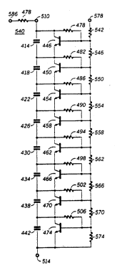
FIG. 10 i_ a circuit sohem~t;c of a circuit, referred to
25 generally by lefelellce numeral 410, and includes eight
capacitors 414, 418, 422,426, 430, 434, 438 and 442 connecte-l in
a series connection therebetween. Circuit 410 of FIG. 10 is
Rimil~r to circuit 290 of FIG. 8, with the substitution of
tr~nRi~t~r r~ ~WUll~ having tr~nci~t~rR 446, 450, 454, 458, 462,
30 466, 470, and 474 for diodes 326-354 of FIG. 8. Each capacitor-
tr~n~i~tor pair (here capacitor-tr~nRi~tQr pairs 414-446, 418-
450,422-454,426-458,430-462,434 466,438-470 and 442-474)
operate in a m~nner ~imil~r to capacitor-diode combination
370-382 of FIG. 9. Circuit 410 of FIG. 10 further illustrates
- 19-
-20 20684 1 ~;
~s;st~rs 478,482,486, 490,494,498,502 and 506 cQnn~cte~
be~ cn the collectQr and base electrodes of tr~nRiPtQrs 446-474
which forms a portion of the re&~ e trAn-Q-istQr networks.
Upon Ap~lic~tion of a charging current to nodes 510 and 514,
5 each capacitor 414-442 is charged with a charging current of
an i-l^ntic~l level. Variances in charge storage r~llQe-l by
variances in c~p~;ve values of capacitors 414-442 are
comp~n~Ate 1 for as increasing potenti~l differences taken
across plates of capacitors 414-442 cause tr~n~Q-iPt~rs 446-474
10 A~ sociAte l therewith incre~Qingly to form shunts to shunt the
charging t ~ellt thereto. Once the charging current source
is no longer applied to nodes 510 and 514,-the charge applied to
capacitors 414-442 is stored thereby. Ber~ e the charge stored
by each of the CPpQ~ lol ~ 414-442 is thereby of a precisely-
1 5 known value, and the potqntiAl dirre~ces across the platesderived thelerrom are also of precisely-known values, the
potent;s~l Jirre~e,lces between nodes 510 and 514 _ay also be
determine~l.
Tun~ing now to the circuit s~h^m~t;c of FIG. 11, a
20 circuit, lefel~ed to generally by lefele.lce numeral 540, is
shown. Circuit 540 is Q;mil~r to circuit 410 of FIG. 10 and
includes ~QimilArly-nllmhered capacitors 414442 connecte 1 in a
series conn~cti~n the~ebel..ecn, transistors 446-474, each
Aqsor~ted with a capacitor 414-442, respect;vely, and resistors
25 478-506 cQnn?ct~-~l between collectQr and base electrodes of
transistors 446474, respectively. Additionally, transistor
b;Aqiru~ c;r~ may be ~d~le~l~ as desired. Circuit 540 of FIG.
11 rul ILC~ in~ e8 resistors 542, 546, 550, 554, 558, 562, 566,
570, and 574 connect~ i in a series conn?- t;Q- theretogether
30 wherein nodes formed between A~ cent ones of the resistors
542-574 are electrically cQnnects~l to base electrodes of
transistors 446-474. A first side of resistor 542 forms node 578.
Resistor 582 is coupled to node 510 at one thereof and forms
node 586 at a seCQn~l side thereof.
- 20 -
20684 ~ 5
- - 21 -
Rs~iators 542-574 form a voltage divider circuit for
supplying bias currents in sddition to, or to offset, bias
c~ule.lts ~lpp~ed by the l~E~ ve resistors 478-506 to
respective base electrodes of tr~na~FtQrs 446-474. A charging
5 current co~-ple l at a first side thereof to nodes 586 (coupled
through resistor 582 to node 510) and 578, and at a seco~ side
thereof to node 514 csuses b;~4ir~ voltages to be present at the
base electrodes of tr~n~i~tQrs 446-474 of valueg co-le~,on~ling
to the resis~,aucea of resistors 542-574. These b ~4ing voltages
1 0 are l,lo~olLional to the voltage at node 586. The voltage divider
circuit comp.;sed of resistors 542-574 forms a h;~a;ng circuit.
By s?lection of large values of resistors 542-574, the
;ng current at resistors 542-574 is of a smsll value relative
to the value of the current supplied to c~p~~itors 414-442 to
1 5 charge the capacitors thereby.
While not sho vn, diodes may further be connect~ at the
nodes h ~. ~.1 adjacent ones of the resistors 542-574 and base
electrodes of tr~n~iPtQrs 446-474 to ~. e~e.lt for n~tinn of
ch~rge paths (such as e.g., through l~s;~tor 478 and then
20 resistors 546-574).
Once the charging current is no longer applied to nodes
510-514, the charge is stored by capacitors 414-442, and the
potentis~l di~elehces across the plates ofthe r~l,e~l:ve
capacitors 414-442 derived thelcrl~ is of known values
25 which, pimil~qrly, may be llt;li7e~l to power a load elçm~nt~
FIG. 12 is a partial circuit srh^m~c~ partial block
diagram of circuit 410 of FIG. 10 connected at nodes 510 and
514 thereof across load elçment~ 600. As described previously,
~pplic~tiQn of a charging current to circuit 410 stores electrical
30 charge upon plates of each of the capacitors 414-442 of the
circuit 410 to generate known potçnti~l differences across each
of the capacitors 414-442, and, hence, a known potenti~l
difference across nodes 510 and 514. When circuit 410 is
connecte~l as illustrated in FIG. 12, fli~h~rge of the stored
- 21 -
- -22- 20684 1 5
ch~ of t_e capacitors 414-442 generates a current to power
load QtemAnt~ 600 thereby. Circuit 410 t_ereby forms a
capacitive power supply rApAhle of generating known levels of
currents and voltages. It is to be noted that circuit 290 of FIG.
5 8, circuit 540 of FIG. 11, and ot_er circuits equivatent thereto,
m ay ~milorly be ll~;li7e~1 to power load device 600 thereby.
T~l~ug now to the block diagram of FIG. 13, a
radiote~lept-Qn?, rcfel,c;t to 6~ue~alty by ~cefele.~ce numeral
604, constructed ac~o~dillg to the teA~hi~ of the pre~ent
10 inven1;~An~ is illustrated. RadiotelA~phr~ne 604 is enclosed by
block 600, shown in hatch, which correspQn~l~ to load elçm~nt
600 of FIG. 12. Suitable connec~ion of ~ telephQne 604 to
nodes 512 . nd 514 of circuit 410 (or, for -Yo,T~rle, to nodes 358
and 362 of circuit 290 of FIG. 8 or to nodes 510 _nd 514 of circuit
1 5 540 of FIG. 11) permits yc.. e.~g of the radiotelephone 604
thereby. The actual ~c~l~ ¢~bG~lg the filnct;on~l blocks
of radiotelephQnes 604 may be ~i~pose~l upon one or more
circuit boards and housed within a co~ ç~t;Qn~ql
~ liotelerhQr~e houging. A transmitted signal transmitted,
20 by, for eY~mple, a base st~t;Qn of a cellular, commllnicsl~;Qn
system, transmits a signal to ~ntenn~ 608. ~ntqnn~ 608
supplies the l~ived signal on line 612 to ~c3ele~lQr/filter 616.
Preselecb~ ;lter 616 is ~Icfelably a very wi~n~l filter
having a p~b~n~l to pass all of the freqllen~ies within a band
25 of interest. Filter 616 generates a filtered signal on line 620
which is supplied to mi_er 624. MiYer 624 also receives an
osr~ ng signal on line 628 which, preferably, is generated by
a conventional phase locked loop. MiYer 624 generates a down
CO.1Ve1 led signal on line 632 which is supplied to filter 636.
30 E ilter 636 generates a filtered signal on line 640 which is
gllpplietl to ~m~lifier 644. ~mplifier 644 generates an
~mplifiPd gignal on line 648 which is supplied to second mixer
652. ~ecQn-l mixer 652 also receives an os~ ng signal on
line 656, which, again, is l,lefelably supplied by a
-23- ~ ~) 6~3~ l 5
cU~vq~t;~nol~ phase locked loop circuit. ~SecQ~ d mixer 652
generates an fieCQn~l down collve~6ion signal on line 654 which
is supplied to Slter 660. Filter 660 generates a Sltered sign~
on line 666 which is supplied to limitnr 670. I~niter 670
5 generates a voltage-limited signal on line 674 which is
supplied to ~e---o~ tion circuit 678. Demo~ t;on circuit
678 d~ .-~l.-lnteE the signal e~pplied thereto on line 674 and
.~elates an o~ ut signal on line 682.
The block diagram of FIG. 13 further illustrates a
1 0 transmit portion of radiotelephone 604 cu ,~l;sing microphone
686, modulator 692, mixer 696, and Slter 700. A Sltered signal
~.~e-ated by filter 700 is s~pplie l to ~nt~nn_ 608 on line 704 to
permit trs~n~mi~sion therefrom.
It is noted that the top portion of the block diagram of
1 5 FIG. 13 also describes a ~ ea;ve~, such as a radio-pager which
may s;mil~rly be ~,. e~c~l by the capacitive power supply of the
eEe.lt invention.
Turning finally to the cut-away, s~he-nstic view of FIG.
14, a portion of the c~spA~tive power supply of the present
20 invention is shown. As m^ t;Qne~l previously, capacitor
~8ignc have been developed which are both of high capacitive
values and low effective seriea resi~tnnC~s FIG. 14 illustrates
eight of such capacitors, refel--ed to by lefe~e~ce numerals
750, 754, 758, 762,766, 770,774, and 778 Lo~ed within
25 8u~ e ho~ ng 782. Each capacitor 750-778 is of
s~hstsntiAlly similAr rlims~ ons and constr~ctiQn~ namely,
each plate is a~ o~;ms-te forty square c~-~t;~-?ters (area) in
lengthwise and widthwise limpn~iorl~ five mils in hPight,
and each plate thereof is c~ ;sed of a ce.a~c cQn~ ve
30 mat,erial to provide a relatively thin power source with a
n~minsl voltage of 1.2 volts, and low, series resist-s-n~e.
~a~ating O~O~illg plates of each capacitor 750-778 is an
aqueous electrolyte, indicated by material 786 co~t-s-inecl within
the internal rhsmber formed of supportive housing 782.
- 23 -
24 20684 1 5
Material 786 may alternately be CO~l ;sed of a nonaqueous
electrolyte or a solid-state cle_~,olyte. Adtitionally, the
surfaces of each plate are rough, uneven, and sponge-like in
appearance, and cQnt~in pores to form porous surfaces
5 thereby.
While the present i,l~ lion has been described in
cQnnect;~n with the ~._fel,ed emho~ t~ shown in the
various figures, it i8 to be understoot that other eimilAr
~ml~lim-n~ may be used ant mc!~lifi~t,~Qn~ and additions
10 may be made to the described eml~o~ e~t~ for l,erfo, llg the
same filnct;on of the present invention without deviating
thelefro. . The,efo~e, the present invention should not be
limited to any single emho~liment, but rather construed in
breadth and scope in accordance with the rcc;talion of the
15 appen-le-l rlAim~
What is claimed is:
- 24 -