Note: Descriptions are shown in the official language in which they were submitted.
cSp- 3&"~
20S8~22
SPECIFICATION
SURFACE LIGHT SOURCE ELEMENT
TECHNICAL FIELD
The present invention relates to a surface light
source element used for a surface light source device, in
particular, to a surface light source element which can be
used as a back light device for a liquid crystal display
element.
TECHNICAL BACKGROUND
Conventionally, a structure which comprises a tubular
lamp as a light source located at the focal point of a
paraboloid of revolution type of reflector and an
opalescent diffusing plate located above the lamp, ls
generally used. Such a device is improved by adjustment of
the shape of the reflector or of the diffusion coefficient
of the diffusing plate.
There exists a device having a combination of a
tubular lamp and a light guide with a shape which is
simulated by an approximation of a point-like source of
light and is formed in the shape of the approximated curve
so that lights in a direction are emitted, a device having
a light guide the thickness of which varies along the
advance direction of light, a device using a lenticular
member having angles of prisms which vary according to the
2 2068422
distance from a light source, and a device having a
combination of these elements.
Recently, surface light source elements have been used
as liquid crystal display elements. However, the display
device, which uses a conventional surface light source
element to obtain a high quality display, requires a thick
surface light source element. In particular, a surface
light source element for a large display of 10 to 12 inches
requires a thickness of 20 to 30 mm. Therefore, it is
impossible to function as a thin surface light source
element.
Various edge-light types of surface light source
devices have been proposed. Each of the devices has a
transparent light guide comprising a plate-shape
transparent material such as an acrylic resin. Light
incident on an edge portion of the transparent light guide
is then emitted from the upper or lower surface of the
light guide. However, such a large liquid crystal display
device with a size of 10 to 12 inches results in a display
with darkness corresponding to the distance from the light
source or an uneven display, so that a display of high
quality cannot often be obtained.
In order to solve this problem, a light guide having a
thickness which varies according to the distance from a
lamp, or a member which varies light path geometrically, is
provided. However, such a member requires a precise
processing to form a specific shape, and high processing
costs. Furthermore, the member provides a low utilization
rate of light.
2068422
Recently, Japanese Patent Application ~aid-open No.
(Tokukai-Hei) 1-245220 discloses a surface light source
element which is an edge-light type. The surface light
source element has a light guide with a layer of a light
diffusing material which is applied or adhered on the
surface thereof opposed to a light emitting surface or on a
light diffusing surface of a provided member. The density
of the provided light diffusing material increases as the
distance from the light incident portion increases.
Japanese Patent Application Laid-open No. (Tokukai-Hei) l-
107406 discloses a surface illuminating device which can
uniformly illuminate the whole surface of a light diffusing
plate. The device has a plurality of piled transparent
plates, each of which has a different pattern of fine dots
(light diffusing material) thereon.
Since a non-light-transmissive inorganic material
(e.g., white pigment such as titanium o:~ide or barium
sulfate) is used, a loss of light occurs to lower the
luminance of the emitted light.
Oe has reported a light diffusing device which
comprises a light guide, a diffusing layer provided on the
light guide through a layer having a middle characteristic
between those of the light guide and the diffusing layer,
and a light regulation member for obtaining a uniform
emitting light on the diffusing layer, in Japanese Utility
Model Application Laid-open No. (Jitsukai-Sho) 61-171001
and in United States Patent No. 4729068.
The inventors have proposed a surface light source
elemer-t which is an edge-light type, as described in
4 2068422
Japanese Patent Application Laid-open Nos. (Tokukai-Hei) 1-
244490 and 1-252933. The element has a lens-like surface
or a satin finished surface provided on at least one of a
light emitting surface of a light guide and the opposed
surface thereof, and a light regulation member having a
light reflecting pattern which corresponds to the
reciprocal of an emitting light distribution and a light
diffusing plate provided on the emitting surface of the
light guide.
The light diffusing device and the surface light
source element using the light regulation member show
excellent effects regarding the uniformity of the emitted
light. The device and the element, however, cannot reuse
the light which is reflected by the emitting light
regulating member, so that the luminance of the emitted
light lowers near the minimum value of the luminance before
regulation.
The object of the present invention is to provide a
very thin type of surface light source element which can
supply emitted light with a uniform and high luminance.
DISCLOSURE OF THE INVENTION
The surface light source element according to the
present invention comprises a transparent light guide ~1)
which has a side end surface as a light incident surface, a
surface perpendicular to the light incident surface as a
light emitting surface, and a light reflecting layer
2068422
provided on an opposed surface to the liqht emittinq
surface; and a diffusing member (2) for diffusinq light
from the light emitting surface of the transparent light
guide; wherein at least one of the light emitting surface
and the opposed surface of said transparent light guide has
a directional light emitting function which radiates the
incident light from the light incident surface of the
transparent light guide in an oblique direction to the
incident light and has a regulation fur,ction which makes
the luminance of the light throuqh the liqht emitting
surface uniform over the whole surface thereof.
Generally, the amount of light from the light emitting
surface which is incident on the light quide decreases as
the distance from the light incidenr surface increases due
to light emitting through the light emittinq surface and
l.ight absorption inside the light quide. In the surface
light source element according to the present invention,
the ratio of the flat areas increases as the distance from
the light incident surface decreases. Therefore, even if
the transparent light guide is thir" it is possible to emit
light with a uniform luminance over the entire emitting
surface on the basis of the incider,t liqht. The incident
light into the transparent light gui~e is not wasted and
has a high utilization rate. Conse~uer;t'y, it is possible
to produce emitted light having a high luminance without
increasing the wattage of the liqht .,ource. Therefore, the
present invention provides a very thin r~pe of surface
light source element which can supplv an emitting light
with a uniform and high luminance.
6 2068422
BRIEF DESCRIPTION OF THE DRAWINGS
FIGS. 1 (a~ and (b) are sectional views showing a
construction of a conventional surface light source
element.
FIG. 2 is a view showing the change of luminance to
the distance from the light incident s~rface of various
kinds of surface light sources.
FIG. 3 is a partially fragmentary and perspective view
showing a back light device incorporating a surface light
source element according to an embodiment of the present
invention.
FIG. q is a partially sectional view taken along line
IV-IV of FIG. 3.
FIGS. 5 (a)-(e) are schematic views showing
embodiments of plan patterns of flat areas.
FIGS. 6 (a)-(c) are schematic sectional views showing
various kinds of lens units.
FIGS. 7 and 8 are partially sectional views showing
modified embodiments of the surface light source element of
the present invention.
FIG. 9 is a schematic side view showing a modified
embodiment of a back light device.
FIG. 10 is a graph showing an area ratio distribution
of flat areas in a pattern formed on a mold for
manufacturing a light guide used for em~odiments of the
present invention.
2068422
FIGS. 11 (a) and (b) are plan views showing a
manufactured light gulde.
FIG. 12 is a graph showing a measurement result of a
luminance distribution of the respective surface light
source elements.
FIG. 13 is a schematic vi,ew showing a method for
measuring directional emitting angles of a manufactured
surface light source element.
FIGS. 14 (a) and (b) are graphs showing a measurement
result of directional emitting angles of a manufactured
surface light source element.
BEST MODE OF CARRYING OUT THE INVENTION
The surface light source element of the present
invention will be described in detai1.
First, the basic principle of a surface light source
element according to the present invention will be
explained. The refractive indexes n of a transition from
light guide to air are approximately 1.4 to 1.6. In the
system of edge-light of which the incident surface 7 is
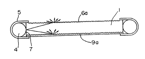
perpendicular to an emitting surface 6 4~ shown in FIG. 1
(a), light theoretically cannot radiate from the emitting
surface 6 when the critical angle of incidence is about
45. In FIG. l(a), the numeral 4 indicates a light source
such as a fluorescent lamp, the numeral 5 indicates the
reflector therefor, and the numeral 2 indicates reflective
8 2068422
surface formed at the opposed side of the emitting surface
6 of the light guide 1.
The emitting surface 6 is generally formed to be a
surface 6a treated in light diffusion or the reflective
surface 2 is formed to a diffusing reflective surface 9a.
The inventors have studied diffusing treatment for at
least the surfaces of a light guide and the opposed surface
thereof, in order to increase the amount of emitted light.
Consequently, it has been found that a method using surface
roughening on these surfaces as uniformly as posslble and a
method using a plurality of lens units for radiating light
in a predetermined direction is effective rather than the
method of using application of a light diffusing material
on at least one of the surface of the light guide and the
opposed surface thereof or the method of using formation of
a light diffusing material layer on the surface when an
acrylic plate is made by polymerization.
A surface light source element which comprises a light
guide with a roughened surface, a fluorescent lamp with a
surrounded silver-evaporated polyester film as a reflector
provided on an end surface thereof, and a white film as a
reflective member provided in contact with the roughened
surface, was made to measure the luminance of the light
emitted therefrom. Consequently, the luminance of the
emitted light decreases as the distance from the
fluorescent lamp increases. When the distance is 70 to 80
times the thickness of the light guide, the luminance is
about 1/10 that at the distance zero. This is shown by the
line 1 in FIG. 2. The inventors have proposed
9 2068422
uniformization of luminance by a light transmissive sheet
for regulating the emitting light in Japanese Patent
Application Laid-open Nos. (Tokukai-Hei) 1-244490 and 1-
252933, as described above.
According to the method, it is possible to make the
luminance of the emitted light uniform. However, this
method lowers the value of luminance of the overall emitted
light to about 1/10 to 1.5/10 of that near the incident end
portion. In this method, utilization of the incident light
energy passing through the light guide was not performed
efficiently. This is shown by the line 2 in FIG. 2. The
reason for this is that the light ~ransmissive sheet for
regulating the emitting light can cut the emitting light
but cannot reuse the cut light because of a regulating
pattern reflecting the light.
Therefore, the inventors have developed a surface
light source element so as to use ~he incident light as
efficiently as possible, in view of the above situation.
In the surface light source element, light emission is not
performed by using the regulating pattern of the light
transmissive sheet for regulating the emitted light, or by
applying a light diffusing material on the opposed surface
of the light emitting surface so that the density of the
material is greater as the distance from the light incident
portion is greater, as disclosed in Japanese Patent
Application Laid-open No. (Tokukai-Hei) 1-245220. In the
surface light source element, a transparent light guide
which was reported in Japanese Patent Application Laid-open
Nos. (Tokukai-Hei) 2-17, 2-84618 and 2-176629 and emits a
1 o 2068422
large amount of light, and an interface for reflection
having a small optical loss of light are used to regulate
the amount of emitted light so as to make the luminance
value on the light emitting surface uniform.
That is, in the surface light source element according
to the present invention, roughened surfaces or a plurality
of lens units, each of which has a directional light
emitting function which radiates the incident light from
the light incident surface of the transparent light guide
at an oblique direction to the incident light, are provided
on at least one of the light emittinq surface and the
opposed surface thereof; and flat areas are provided on the
roughened surfaces or the plural lens units so that the
ratio of the flat areas thereon increases as the distance
1 from the light incident surface decreases, thereby the
transparent light guide has a regulation function which
makes the luminance of the light through the light emitting
surface uniform over the whole surface thereof.
Accordingly, it is possible to increase the value of
luminance of overall emitted light to about 3/10 of that
near the incident end portion and to obtain a surface light
source element showing a uniform luminance valùe over the
entirety of the light emitting surface. This is shown by
the line 3 in FIG. 2.
EMBODIMENT
The surface light source element of the present
invention will be described concretely via the embodiments.
2 0 ~ 2
1 1
Surface light source element
FIG. 3 shows an embodiment of a back light device
incorporating a surface light source element according to
the present invention. FIG. 4 shows a partially sectional
view taken on line IV-IV of FIG. 3.
The device comprises a light guide 1 with a
rectangular plate shape, a film-like light diffusing member
3 provided over the light emitting surface 6 thereof, a
light source 4 such as a fluorescent lamp provided on the
side end surface (a light incident surface 7) of the light
guide 1, and a reflector 5 for holdir,g the light source 9
and reflecting light to the incident surface by the
reflective surface provided on the inner surface thereof.
The opposite side of the light emitting surface 6 of the
light guide 1 has a light reflective layer 2.
The surface light source element according to the
present invention is characterized ir, that roughened
surfaces or a plurality of lens units, each of which has a
directional light emitting function which radiates the
incident light from the light incident surface of the
transparent light guide in an oblique direction to the
incident light, are provided on at least one of the light
emitting surface and the opposed surface thereof; and flat
areas are provided on the roughened surfaces or the plural
lens units so that the ratio of the flat areas thereon
increases as the distance from the light incident surface
decreases, thèreby said transparent light guide has a
regulation function which makes the luminance of the light
,~ 2068~22
through the light emitting surface uniform over the entire
surface thereof.
In thls embodiment, flat areas 8 are provided on the
roughened opposed surface 9 to the light emitting surface
6, so that the flat areas 8 are more numerous as the
distance from the light incident surface 7 decreases, as
shown by arrow A in FIG. 4.
The increasing ratio of the flat areas in the light
guide can be selected, changed and determined appropriately
according to the shape or pattern of the flat areas, the
material or shape of the light guide, the kind of the light
source, the treatment degree of the light emitting or
reflecting surface or the like.
Pattern examples of the flat areas are shown in FIGS.
5 (a) to ~e). In every example, the area ratio of the flat
areas 8 becomes increases as a position is nearer the light
incident surface 7, as shown by arrow A in FIG. 5.
The diffusing member 3 which can be used for the
present invention may be any structure or material which
can diffuse light from the light guide nondirectionally.
The diffusing member 3 can be provided on the light guide 1
by the end portion of the light guide adhering to the
diffusing member 3 by an adhesive, by compulsory close
contact through pressure, or by merely positioning the
diffusing member 3 on the light guide. Furthermore, it is
possible to laminate the light guide 1 and the diffusing
member 3 directly or through a layer of air.
The light guide 1 in the present invention can be
obtained by a transparent resin such as an acrylic resin, a
13 2068422
polycarbonate resin or a vinyl chloride resin. In
particular, it is preferable to use an acrylic resin having
a large transmission coefficient of visible light. The
method of molding the light guide 1 can be selected or
changed appropriately.
The light source 4 in the present invention is not
limited. A fluorescent lamp or a filament lamp which is a
continuous tubular light source, a plurality of point-like
sources of light arranged along the incident surface, or a
light source device comprising a combination of a light
transmissive member which can receive light through a side
surface and a light source provided near the end portion
incident surface of the light transmissive member, can be
used as a light source.
The reflecting layer 2 of the surface light source
element according to the present invention can be formed by
laminating a reflecting film or the like which comprises a
film and an evaporated metal such as Ag, Al or the like.
It is preferable to use a reflecting material having a high
reflectivity.
In this invention, the light guide requires at least
one of the light emitting surface 6 and the opposed surface
being roughened, or a plurality of lens units being formed.
Furthermore, it is necessary to provide flat areas on the
roughened surface or on the surface on which a plurality of
lens units are formed, so that the ratio of the flat areas
thereon increases as the distance from the light incident
surface decreases.
14 2068422
In a preferred embodiment of the present invention,
the surface of the flat areas 8 in the light guide 1 is
preferably an optically flat surface, in particular, to be
a mirror surface. The incident light with an incident
angle more than the critical reflective angle to the
optical flat surface can be reflected almost without loss.
Since the light does not leak, it is possible to use
the light effectively to increase the luminance of the
entire light emitting surface.
The shape of the lens unit which is used in the
present invention is not limited. For example, a lens unit
with a shape proposed in Japanese Paten~ Application Laid-
open No. (Tokukai-Hei) 2-17 by the ir,ventors can be used.
Lenses 20 having various shapes are shown in FIGS. 6~a) and
(b).
The roughened surface which is used in the present
invention preferably has a haze value of not less than 30~,
and more preferably, not less than 50- in the roughened
surface portion.
The surface light source element according to the
present invention is not limited to the above embodiment.
Various changes or modifications in form and details may be
made therein. For example, in the above embodiment, flat
areas 8 are provided on the roughened surface 9 opposed to
the light emitting surface 6. However, flat areas 8 can be
provided on the roughened light emitting surface 6, as
shown in FIG. 7. It is possible to provide a structure so
that the area ratio of the flat areas thereon increases as
2068~22
the distance from the light incident surface 7 decreases,
as shown by arrow A in FIG. 7.
Furthermore, it is possible to provide the flat areas
on both roughened surfaces of the light emitting surface 6
and of the opposed surface 9, as shown in FI~. 8. It is
possible to provide a structure so that the area ratio of
the flat areas thereon increases as the distance from the
light incident surface 7 decreases, as shown by arrow A in
FIG. 8.
In the above embodiment, the light source 4 is
provided only on one end side of the light guide 1. It is
possible to provide the light source 4 on both ends sides
of the light guide 1, as shown in FI~. 9.
Reaulating method of the surface liaht source element
The surface light source element according to the
present invention can be regulated and manufactured by
various kinds of methods.
For example, when the flat areas are provided on a
roughened surface of the light guide or on a surface having
lens units, it is possible to manufacture desired light
guides by using a method in which flat areas are provided
on a roughened surface or on a surface having lens units or
by using a method in which roughened parts or lens units
are provided on a flat surface.
A die having a desired roughened pattern or a surface
roughness, or a die having specific lens units and flat
areas is prepared by surface roughening treatments such as
sandblasting, etching or the like. A light guide, which
16 2 0 6 8 ~ 2 2
has predetermined flat areas on at least one of a light
emitting surface having a roughened surface or lens units
and an opposed surface thereof, can be obtained by an
injection molding of a resin or by a heat-press using such
a die. In particular, the injection molding method is
preferable because of high precision and high molding
speed.
The manufacture of the surface light source element
can be performed by preparation of necessary members such
as a light guide, a diffusing member, a reflecting material
and the like, and by then assembling them.
Detailed embodiment
(Manufacture of a die for a light quide)
Glass beads were blown on a polished surface of a
brass plate, so that a metal plate on which surface
roughening is carried out by a usual forming process was
manufactured (Die 1).
A gradation pattern having a distribution of area
ratio of the flat areas as shown in FIG. 10 was formed by
using CAD. A pattern was developed and printed photo-
optically on the surface of the Die 1 by a usual
photolithography process. The portion to remain as
roughened surfaces, that is the portion similar to the
rough parts 22 as shown in FIG. 11(a), was protected by a
film. The remaining portion was polished to a degree of
roughness with an emery-paper No. 800. Thereafter, a die
having predetermined flat areas was made by removing the
protecting film (Die 2).
17 2068~22
A surface of a brass plate was polished by a buff with
an emery-paper No. 800, and then a mirror plate was made
(Die 3)-
A combined die for injection molding which had onesurface with a state similar to that of the Die 2 and had
the other surface with a state similar to that of the Die
3, was made (Die 4).
(Manufacture of a light guide)
An acrylic resin plate of 150 mm :: 250 mm with a
thickness of 3 mm was sandwiched between the Die 2 and the
Die 3 and a replica was formed by a conventional heat-press
process. Then, the replica was cut to the size and pattern
position as shown in FIGS. ll(a) and (b). The four cut
sides were polished to have mirror surfaces in a
conventional manner (Light guide 1).
In FIG. ll(a), numeral. 22 indicates roughened surface
parts. In FIG. ll(b), the light guide 1 has a length (B)
of 225 mm, a width ~C) of 132 mm, a width of a zone "0" (D)
of lS mm, an effective width (E: a width of zones "1" to
"11") of 205 mm, and a width (F) of zone "12" of 5 mm.
An acrylic resin plate of 150 Inm :~ 250 mm with a
thickness of 3 mm was sandwiched betweer, the Die 1 and the
Die 3 using a process similar to the above process and a
replica was formed by heat-pressing. Then, the replica was
cut and polished to produce a light guide (Light guide 2).
A negative EP picture was made as a comparative
example so that ink could be applied on the rough
corresponding parts of the Die 2 by a screen printing
18 2068422
process. A print form for screen printing was made by
using this. Screen printing was carried out on a surface
of an acrylic resin plate of 150 mm x 250 mm with a
thickness of 3 mm using a commercially available white ink
(VIC 120 White made by Seiko-Advance Co., LTD.).
Thereafter, this was cut and polished in a similar manner
to that of the light guide 1 or of the light guide 2 to
make a light guide for comparison (Light guide 3).
Light guides were made from acrylic resin pellets
(Acrypet VH made by Mitsubishi Rayon Co.) at a cylinder
temperature of 240C by using a 200 t-injection molding
machine and the Die 4.
(Measurement of the haze value of the light guide 2)
Pieces of sample of 50 mm x 50 mm were cut out from
the roughened surface parts of the light guide 2, and the
haze value thereof was measured according to ASTM-D 1003-
61. The haze value was calculated according to the
following equation.
Haze value = ~(Transmittance of diffused light) /
(Total transmittance light)) ~. 100~
Consequently, the haze value of the light guide 2 was
64.8.
~Assembly of the surface light source element)
A crystal white plate produced by Sky Aluminium Co.
(an aluminum plate with a thickness of 0.25 mm, a surface
of which is coat~d with a white paint) was positioned in a
folded state with an inner white surface so that the plate
2 0 6 8 4 2 2
had a rib with a width of 3 mm and a flat portion with a
size of 132 mm x 225 mm. At least one of two short sides
had no rib, so that the short side can function as a light
incident surface. This plate is the light reflecting
member. A milk white polyethyleneterephthalate film "EK
300 W" produced by Somar Co., with a thickness of 0.075 mm,
was cut to size of 132 mm x 225 mm to use as a diffusing
member.
A cylindrical member having an inner diameter of 6 mm
and a crystal white inner surface was produced as a lamp
case. The lamp case has an aperture with an opening width
of 3 mm.
The light guide was placed on the light reflecting
member so that the "O" zone as shown in FIG. ll(b) was
adjacent to the short side without rib of the light
reflecting member and the roughened surface or the printed
surface was close to the white surface thereof. The
diffusing member was placed on the light guide. These
three members were inserted into the aperture of the lamp
case together. A lamp "KC 130 T4E74" produced by
Matsushita Electric Industry Corporation with a diameter of
4 mm and a length of 130 mm was set in t he lamp case as a
surface light source element. "CXA-LlOL" produced by TDK
Corporation was used as an inverter for lighting a lamp.
The lamp was lighted by application of DC 12V.
(Measurement of luminance of the surface light source
element)
2068~22
Luminance of the surface light source element was
measured by a luminance meter "BM-5" produced by Topcon Co.
through a view angle of 1 and a measurement circle of 10
to 15 mm in diameter. The measurement was carried out at
the central portion of the zones "1" to "11" as shown in
FIG. 11. The surface light source element was fixed at a
predetermined measurement pedestal perpendicularly thereto
so that the lamp was in an upper side. After lighting had
been carr'ed out by application of DC 12 V, the measurement
was carried out through a lamp aging time of more than 15
minutes. The condition of temperature for measurement was
23C i 2C.
~Result of luminance measurement)
Results of the luminance measurement is shown in Table
1 and FIG. 12.
21 20~8~22
Z o _ o _ o _ _
c~> _ ~ c~ ~ ~ o 0 0 r-
o o o o o o o o o o
~ ., o` o . o . ~ ~. . . o
~ H ~ ~ _ _ _ . ~ ~ c~ _ _ ~
~ 0~ _ _ _
o ~ C~ C_ 0 <o ~ o 0 o o
C~ _ _ o o o o o o o o o o
_ O _ _ _
~ H u~ o o ~ o .~- o 0 ~_ ~ ~ 7 ~_
_~ ~ . _ ~ ~ _ _
~ OZ C-~ ~_ ~ o oD _ _ o r- ~r ~
~) ~ 0 ~ ~ ~ O> O> O O> C7> CJ>
F _ _ _ ~ _ ~ ~ _ _ _
Z ~" _ ~ ~ t- .,o ~ o 0 ,_ ,_ .
- - - - -
~ _ c~ c~ ~r u~ ~ r- ~c a~ o _ S~
o - - - - ~
` 22 2~68~22
According to the light guide l which is an embodiment
of the present invention, it is possible to ra~iate emitted
light with an approximately uniform luminance over the
whole of the light emitting surface and to illuminate a
display surface with a uniform luminance. The light guide
1 has a utilization rate of light higher than that of the
light guide 3. Therefore, even if the same light source is
used, it is possible to obtain emitted light having a high
luminance. The surface light source element using the
light guide 4 can provide a result similar to that of the
surface light source element using the light guide 1.
(Measurement of directional emitting angle of the light
guide)
A sample was placed on a measurement pedestal so that
a lamp y was at the left side. The luminances at
predetermined angles were measured, rotating the sample as
shown in FIG. 13.
A sample in which a diffusing member was removed from
a surface light source element using the light guide 1 is
indicated as 1-1. A sample with a diffusing member is
indicated as 1-2.
A sample in which a diffusing member was removed from
a surface light source element using the light guide 3 is
indicated as 3-1. A sample with a diffusing member is
indicated as 3-2.
The measurement position was fixed at the central
portion of the zone 6 as shown in FIG. 11. The results are
shown in FIGS. 14(a) and (b).
2068422
23
UTILIZATION POSSIBILITY IN INDUSTRY
As described above, in the surface light source
element according to the present invention, at least one of
the light emitting surface and the opposed surface of said
transparent light guide has a directional light emitting
function which radiates the incident light from the light
incident surface of the transparent light guide at an
oblique direction to the incident light and has a
regulation function which makes the luminance of the light
uniform over the light emitting surface in the whole
surface thereof. Therefore, even if the transparent light
guide is thin, it is possible to emit liaht with a uniform
luminance over the entire emitting surface on the basis of
the incident light. The incident light into the
transparent light guide is not wasted and has a high
utilization rate. Consequently, it is possible to produce
an emitted light having a high luminance without increasing
the wattage of the light source. Therefore, the present
invention provides a very thin type of surface light source
element which can supply emitted light with a uniform and
high luminance.