Note: Descriptions are shown in the official language in which they were submitted.
2068443
The present invention relates to an opto-elec-
tronic component for optical communications systems, and
more particularly to a gain-coupled distributed-feedback
semiconductor laser to be used as a source in such a
system.
In optical communications systems, and more
particularly long-haul communications systems, sources
capable of emitting single-frequency signals are preferred
in order to reduce, to the greatest extent possible, signal
distortion due to the different propagation rates of
different frequencies. Single-frequency emitting sources
are essential in coherent communications systems and for
high-speed direct source modulation.
Examples of single-frequency emitting sources are
semiconductor lasers in which optical feedback is obtained
through the use of mechanisms other than multiple reflec-
tions between the mirrors delimiting the laser cavity. In
such lasers, selection of oscillation frequencies (or
modes) is obtained without resorting to external compo-
nents, so that they may be fabricated by integrated-optics
circuit technology. In addition, the absence of end
mirrors allows such lasers to be integrated with other
components in an optical communications system. Examples
of such lasers are Distributed Bragg Reflector (DBR) lasers
and Distributed-Feedback (DFB) lasers. DFB lasers are
simpler to manufacture and hence are presently preferred.
Generally, in ~FB lasers, optical feedback
results from a periodic spatial variation in the effective
refractive index (i.e. the refractive index presented by
the whole structure for the guided radiation) in the
direction of light propagation, namely the longitudinal
direction. This variation is caused by a grating extending
across the whole cavity on or beneath the laser's active
layer. This optical feedback mechanism is commonly known
as "index-coup1ing" and exploits the t~ct that each refrac-
2068443
-
-- 2 --
tive index change is accompanied by a weak reflection in
the guided radiation. By selecting a suitable grating
period back reflection will occur such that the grating
will act as a wavelength selective mirror. The grating
only reflects light having wavelengths which closely
satisfy the Bragg condition, which is defined as follows:
= m ~B (1)
2nv
where:
o ~ = grating period;
AB = Bragg wavelength;
m = grating order; and
nv = mode refractive index.
In practice, ~B is chosen so as to be coincident with the
emission wavelength of the laser's active layer.
However, index-coupled DFB lasers are not per se
monomode sources, and their behaviour, with respect to
emitted modes, is highly sensitive to reflections on the
end facets. More particularly, if those facets are left
untreated, the oscillation modes of the laser will depend
on the relative positions of the facets with respect to the
grating spatial phase, the position of which is unpredict-
able, since it is impossible to exactly determine at which
point a grating will be cut when manufacturing the individ-
ual devices. If the laser facets are covered with anti-
reflective coatings, the laser will steadily oscillate in
two modes, symmetrical with respect to the Bragg wave-
length. Monomodality can then be achieved by causing the
rays propagating in the laser to undergo a quarter-wave
phase shift in the central grating zone. This phase shift
can be obtained by eliminating a groove of the grating in
the central grating zone, a rather complicated procedure
from a technical perspective. The expense involved in
2068443
-- 3
manufacturing such lasers, by applying anti-reflective
coatings to the facets and manufacturing a grating with the
required phase shift, makes it preferable to keep only
those lasers which as initially fabricated have monomode
structures and to discard the remainder. Notwithstanding
the fact that a considerable proportion of the production
is discarded, this method of manufacturing monomode lasers
continues to be economically advantageous.
The high cost associated with manufacturing
monomodal index-coupled DFB lasers can be avoided by manu-
facturing a DFB laser, in which a longitudinal periodic
gain variation ("gain-coupling") occurs instead of a peri-
odic refractive index variation. In H. Kolgenick, C. V.
Shank, "Coupled Wave Theory of Distributed Feedback
Lasers", Journal of Applied Physics, Vol. 43, No. 5, May
1972, it was theoretically shown that a gain-coupled DFB
laser is intrinsically a monomode structure and is rela-
tively insensitive to facet reflections. Therefore, the
manufacture of a gain-coupled DFB does not necessitate the
expensive procedures required to introduce a phase-shift in
the grating and to apply anti-reflective coatings.
An example of a gain-coupled DFB laser is
described in Y. Luo et al., "Gain-Coupled DFB Semiconductor
Laser Having Corrugated Active Layer" presented at the
International Conference on Solid State Devices and
Materials, Tokyo, August 1988, paper 20DPB-2, and published
on pages 328-330 of the proceedings of the Conference.
This paper describes a GaAs/GaAlAs laser, comprising a
corrugated layer or grating ("pattern providing layer"~
between conventional confinement layers of GaAlAs ("lower
and upper claddings"). The pattern providing layer is also
made of GaAlAs, but with such relative proportions of the
constituent elements as to give a refractive index which is
higher than that of the lower and upper claddings and is
2068~3
close to that of the active layer. The grating is followed
by a further corrugated layer, made of GaAlAs ("buffer
layer"), whose refractive index is slightly higher than
that of the lower and upper claddings. The active layer of
undoped GaAs is deposited on the buffer layer, so that a
planar structure is obtained. In this way~ a periodic
thickness variation is obtained which causes a periodic
gain variation. The refractive indices of the various
layers and the heights of the teeth of the pattern provid-
ing layer and the active layer are chosen so that theeffective refractive index is constant in the longitudinal
direction; thereby obtaining a laser with pure gain-coup-
ling.
This known structure has a number of disadvan-
tages due to the presence of a massive active layer~ whichdoes not permit the attainment of high values for both the
absolute gain and the differential gain (dg~dN~ where g =
absolute gainJ N = number of the injected carriers). It is
well known that the higher the differential gain, the
better the spectral line-width characteristics of the laser
and, generally, the better the dynamic properties of the
device (frequency behaviour, frequency modulation, etc.).
It is known in the art that a quantum structure
yields a gain which is several times greater than that of
a continuous structure (3 to 4 times higher in case of
quantum wells and even higher in the case of wires) and,
moreover, it yields a better differential gain. As a
consequence, relatively high output powers as well as good
dynamic properties can be achieved. Furthermore, it is
known in the art to use quantum structures, and more
particularly multi-quantum well structures, in the active
layers of coupled-index distributed-feedback semiconductor
lasers. However, as mentioned above, it is difficult to
achieve monomodality with these lasers. In addition,
2068443
-
-- 5 --
modification of previously deposited active material in
order to obtain a structure similar to that suggested, with
a plurality of discrete multi-quantum wire structures, is
impractical, since any intervention on the active material
causes the occurrence of faults (more particularly, non-
radiative recombining centres) in the device.
To overcome the above-mentioned disadvantages the
present invention is directed towards a semiconductor laser
and a method of fabricating a semiconductor laser, having
no massive layer of active material and being capable of
achieving good performance in terms of absolute and differ-
ential gain.
In a laser according to the invention, active
material is present only in grating grooves and consists of
discrete layers alternated with layers of a passive
material with a wider band gap. In each groove, the active
and passive layers form the wires and the barriers, respec-
tively, of a multi-quantum wire structure, orientated
perpendicularly to the direction of light propagation.
The invention also provides a method of fabricat-
ing such a laser which comprises the step of: growing in
each groove of the grating a plurality of layers of active
material alternated with layers of a passive material with
a wider band gap so as to form a multi-quantum wire struc-
ture orthogonal to the direction of light propagation.
These active and passive layers form the wires and the bar-
riers, respectively, of said structure.
These and other features of the invention are
further described below with reference to a preferred
exemplary embodiment thereof shown in the annexed drawing
which is a longitudinal sectional view of the laser in
accordance with the invention.
- 20684~3
-- 6
Although the present embodiment of the invention
describes a laser made of InP/InGaAs/InGaAsP, it will be
understood that the description is also applicable to a
laser using different constituent elements, e.g.
GaAs/GaAlAs.
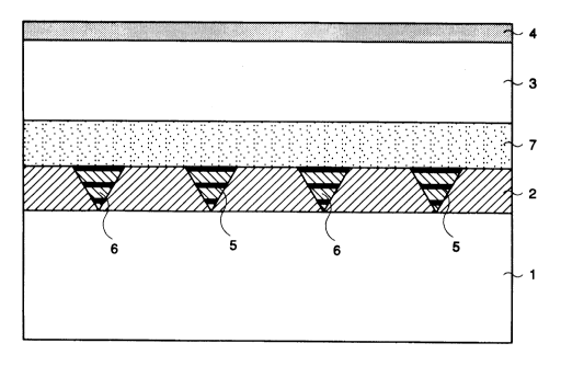
Referring to the annexed drawing, the laser of
the invention comprises, in a conventional manner, a
substrate 1 of suitably doped InP (e.g. n-doped), a grating
2 of quaternary InGaAsP alloy, an upper cladding 3 of InP,
doped in an opposite manner to the substrate 1 (hence p-
doped), and a contact layer 4 of highly-p-doped InGaAsP,
permitting electrode application. The grating 2 has a
period satisfying the above mentioned Bragg condition. In
addition, the constituent element proportions in the
quaternary alloy, of which the grating is made, are chosen
so as to yield a refractive index satisfying specific
conditions which will be described below.
Optically active material is present only in the
grating grooves and consists of discrete layers 5 of
InGaAs, separated by layers 6 of a passive material having
a wider band gap, e.g. InP or an InGaAsP alloy. The layers
5 and 6 are made so as to form the wires and the barriers
of a quantum wire structure, respectively. The thicknesses
of the layers of the active material are chosen so as to
provide the desired emission wavelength (e.g. 1.55 ~m).
This thickness can be accurately determined once the
materials forming the wires and the barriers are deter-
mined.
The number of layers of active material 5 is
chosen at the design stage so as to optimize the laser's
performance. More particularly, the number of layers of
active material 5 is chosen so as to meet the so-called
threshold condition, according to which mode gain must be
20684~3
equal to losses. This condition is expressed by the
following relation:
r g = ~t ~2)
where:
r = optical confinement factor, i.e. the part of the
electromagnetic field contained in one layer;
g = active material gain: and
~t = total losses.
It is known that the active material gain of a
quantum structure is a few times higher than that of a
massive structure; whereas the confinement factor is lower.
By varying the number of the layers one can thereby change
the confinement factor so as to satisfy the above condition
(2).
When an increase in the optical confinement
factor is desired, a further layer 7 of quaternary InGaAsP
alloy can be provided on the grating and the quantum wire
structure. The thickness of this layer 7 is determined at
the design stage in order to increase the confinement
factor and to facilitate the achievement of the threshold
condition (2).
It is clear that the described str~cture presents
a periodic gain variation, since the active material is
present only in the grating grooves. Fabrication of the
active layer as a multi-quantum wire structure ensures the
advantages associated with absolute and differential gain
inherent in this type of structure.
In order to fabricate the laser described, a
grating 2 is formed with the techniques commonly used in
Z068~3
DFB laser fabrication (more particularly holography or
electron beam lithography), then quantum wires are grown in
the grating grooves. In this respect, the techniques
commonly used to fabricate quantum well or quantum wire
structures can be adopted, e.g. molecular beam epitaxy or
vapour phase deposition (or vapour phase epitaxy) of
organometallic compounds. Care is required in order to
ensure the quantum structures are grown only in the grooves
or at least to ensure the easy removal of material of such
structures grown outside the grooves. For example, if the
surface of the grating 2, in zones between grooves, is kept
covered, during the operations leading to the growth of the
quantum structures, with a photoresist layer applied during
etching operations, the material of quantum structures
possibly grown on such layer has a polycrystalline struc-
ture instead of a crystalline one, and hence is easy to
remove, as is well known to persons skilled in the art.
It is important to avoid growth of quantum
structure material on the groove's walls since that would
cause active material continuity inside the groove and
hence would diminish the advantages derived from the
presence of a discrete structure. This growth can be more
readily avoided if the grooves, instead of being exactly V-
shaped, have a non zero width in the zone corresponding to
the vertex. The successive layers are then made in a fully
conventional manner. In addition, lateral light confine-
ment is obtained in a conventional manner, by making a
ridge structure or a buried structure.
To ensure monomodality, the laser must present
gain-coupling alone, without index-coupling. In order to
achieve this, the grating material composition must be
chosen such that the effective refractive index n in the
zones where there are no quantum structures satis~ies the
following relationship:
2068443
n = N~-tw-nw + Nb-tb-nb
(3)
NW-tW + Nb-tb
where:
Nw and Nb are the number of quantum wires and barriers,
respectively;
tw and tb are the wire and barrier thicknesses respectively;
and
nw and nb are the refractive indices of the wires and
barriers respectively.
It is al~ays possible to find a quaternary
InGaAsP alloy with a refractive index n that satisfies the
above relationship (3), since, as is commonly known, the
refractive index in such alloys varies with continuity from
the value corresponding to InGaAs to that corresponding to
InP when varying the proportions of Ga, As and P. The
above relationship (3) clearly indicates that, when a
quaternary InGaAsP alloy is used to make the barriers, its
composition shall be different from that of the alloy used
for the grating.
The above description also applies to lasers made
of GaAs/GaAlAs, in which case the quantum wires 5 will be
made of GaAs and the barriers 6 of GaAlAs. The grating 2,
in order to satisfy the above relationship (3) for the
refractive index, will be made of a GaAlAs alloy of a
composition capable of yielding a lattice parameter differ-
ent from that of the layer on which it is grown ("strained~
material).