Note: Descriptions are shown in the official language in which they were submitted.
2~684~
TEX822/4-9 PATENT APPLICATION
COMPUTER WITH SYSTEM
MONITORING FEATURES
TECHNICAL FIELD OF THE INVENTION
This invention relates in general to computer
technology, and more particularly to a computer with
system monitoring features.
TEX822/4--9 8 ~ ~ 9 PATENT APPLICATION
~AC~GRoUND OF THE INVENTION
Computer technology has become greatly pervasive in
all a6pects of current-day activities. Specifically,
computers are used in applications such as personal u~e,
business use, and industrial applications. One industry
which has become highly computerized is that of
telecommunications. For example, telecommunication
switching is now accomplished via highly sophisticated
switching networks. These switching networks are
commonly constructed by interaction of a series of
computers which accomplish various different functions
necessary to perform the telephone switching operation.
Indeed, under current technology, a typical
telecommunications switch may include on the order of
eight to twelve different computing devices.
For many computer uses, and specifically in the
field of telecommunications, it has become highly
desirable, and often mandatory, to ensure maximum
20 operational time of its various computers. Further,
certain computers within a telephone switching network
are more important to the switching function than others.
As a result, these certain computers may be critical to
the ongoing operation of the system and, therefore, any
downtime of one of these critical computers can adversely
affect the entire communications system. Naturally, an
extensive discontinuation of operation of one of these
critical computers could have devastating effects due to
the interruption of the communications link. For
example, needed communications may be unavailable for
emergency, business and other public or private
- institutions. Further, this interruption could cause
other adverse effects including large economic losses as
well. Clearly, the extent of the losses would depend
upon the particular use of the communications media.
., ,. ._, . .
TEX822/4-9 2 ~ 6 8 ~ ~ ~ PATENT APPLICATION
It iB therefore an object of the present invention
to provide a computer with system monitoring features to
increase the dependability of the computer.
It is a further object of the present invention to
provide a series of monitoring features in a computer in
order to constantly monitor errors which may occur in the
operation of the computer.
It is a further object of the present invention to
provide specific preferable responses to various
different types of errors once they have occurred in a
computer.
It is still another ob;ect of the present invention
to provide various different types of perceivable outputs
in response to the detection of an error. For example,
these outputs may be audio, visual or computer-readable.
It is still another object of the present invention
to provide integrated system components which may be
quickly replaced in the event of a significant failure,
thereby minimizing the downtime of the unit.
Other objects and advantages of the present
invention will be apparent to those of ordinary skill-in-
the-art, having reference to the following specification,
together with its drawings.
2~8l~9
TEX822/4-9 PATENT APPLICATION
SUMMARY OF THE ~ NTION
In accordance with the present invention, a computer
with æystem monitoring features is provided which
substantially reduces the disadvantages and problemh
associated with prior computers, and seeks to further the
objects set forth above.
The present invention in one embodiment includes a
computer with a housing. Within the housing i~ a
motherboard having a central microprocessor. At least
one fan is included for circulating air through the
housing. Various circuitry are also provided, including
circuitry for monitoring the operation of the fan and
circuitry for monitoring the temperature within the
housing. Also included are circuitry for monitoring a
periodic signal provided by the central microprocessor
under normal operation conditions, and circuitry for
presenting a microprocessor error indication to a user if
the periodic signal does not occur within a predetermined
time period.
The present invention in a second embodiment
includes a motherboard having a central microprocessor
and an input for receiving a supply voltage. A circuit
is breaker connected to the input and has an output for
- 25 providing an output supply voltage. Further included are
circuitry connected to the input for monitoring the
existence of the said supply voltage, and circuitry
connected to the output for monitoring the existence of
the output supply voltage.
TEX822/4-9 2 ~ ~ ~ Ll 6 ~ PATENT APPLICATION
BRIEF DESCRIPTION OF THE DRAWIMGS
For a more complete understanding of the present
invention, and the advantages thereof, reference i8 now
made to the following descriptions taken in con~unction
with the accompanying drawings, in which:
FIGURE 1 illustrates a frontal perspective view of a
rack-mountable computer having its top cover removed;
FIGURE 2 illustrates a rear perspective view of the
rack-mountable computer illustrated in FIGURE l;
FIGURE 3 illustrates a schematic of certain
components from the malfunction detection board
- illustrated in FIGURE 1, including the microproce6sor,
program memory, two RS-232 ports, and supporting
circuitry;
FIGURE 4 illustrates a schematic of certain
components from the malfunction detection board
illustrated in FIGURE 1, including voltage comparators
for monitoring different voltage levels, a temperature
sensor, and detection circuitry for monitoring the status
- of two fans used in the computer illustrated in FIGUREs 1
and 2;
FIGURE 5 illustrates a schematic of certain
components from the malfunction detection board
illustrated in FIGURE 1, including a connector and drive
circuitry to drive an LED display, and a connector for
providing various external signals which may be accessed
for remote notice of an error detection and to reset the
- microprocessor illustrated in FIGURE 3;
FIGURE 6 illustrates a schematic of certain
components from the malfunction detection board
illustrated in FIGURE 1, including circuitry for pulling
up various potentials to a level of VCC, a battery
recharge circuit, circuitry for resetting the general
microprocessor associated with the computer of FIGUREs 1
and 2, and power conversion circuitry for converting the
TEX822/4-9 2 a ~ 3 PATENT APPLICATION
input bias voltages (either from a power supply or a
battery) to a sufficient level for VCC:
FIGURE 7 illustrates a series of bypass capacitors
for purposes of removing noise out of the voltage supply
levels of the malfunction detection board illustrated in
FIGURE 8;
FIGURE 8 illustrates a perspective view of the
malfunction detection board disposed within the computer
illustrated in FIGUREs 1 and 2: and
FIGURE 9 illustrates a 6chematic of a power supply
interface board for coupling a power supply board
as60ciated with the computer of FIGUREs 1 and 2 to the
malfunction detection board illustrated in FIGURE
above.
TEX822/4-9 2 ~ PATENT APPLICATION
DETAILED DESCRIPTION OF THE IN~ENTION
The preferred embodiment of the present invention
and its advantage~ are best und,erstood by referring to
FIGUREs 1-~ of the drawings, like numerals being used for
like and corresponding parts of the various drawings.
FIGURE 1 illustrates a frontal perspective view of a
computer in accordance with the present invention, and
designated generally at 10. Computer 10 has a housing
which includes a front panel 12, a left-side panel 14, a
right-side panel 16 and a rear panel 18. Side panels 14
and 16 each includes a grid of holes for permitting air
to pass through the housing of computer 10. In the
preferred embodiment, front panel 12 includes a left and
right handle 20 and 22, respectively, for insertion and
removal of computer 10 into a rack (not shown). Front
panel 12 further includes two disk drive bays 24 and 26,
respectively. Disk drive bays 24 and 26 are constructed
in accordance with principles known in the art in order
to accommodate either half-height or full-height disk
drives. As a result, either floppy disk or hard disk
drives may be disposed within bays 24 and 26, and are
electrically connected to the hardware within computer
10 .
Front panel 28 also includes a test/indicator panel
28. As discussed in much greater detail below, computer
10 of the present invention includes a multitude of
system monitoring features which continuously monitor the
operation of numerous aspects of the computer's
operation. Panel 28 provides one of several mechanisms
for indicating to an operator the results of some of
these ongoing monitoring activities. Thus,
test/indicator panel 28 includes various indicators, as
well as an input button. Specifically, panel 28 includes
two status indicators 30 and 32, indicating an active
status and a standby status, respectively. Panel 28
TEX822/4-9 2 ~ PATENT APPLICATION
further includes a microprocessor indicator 34. Finally,
panel 28 includes three alarm indicators 36, 38 and 40
for purpose~ of indicating the condition of the power
input/breaker, the fans, and the power output,
respectively.
In the preferred embodiment, each of evenly numbered
indicators 30-40 are LED indicators. More specifically,
indicator 30 is colored green, indicator 32 i~ colored
yellow, and indicators 34, 36, 38 and 40 are colored
red/green, depending on the state of the indicator. In
addition, panel 28 includes a lamp-test button 42 which,
when depressed, causes indicators 30-40 to illuminate in
order to assure their proper operation. In the preferred
embodiment, this test causes single color LED indicators
to illuminate while the multi-color LED indicators flash
alternately (e.g., between red and green).
The preferred indications of evenly-numbered
indicators 30-40 is as follows. Active indicator 30 is
on (green) when no failure has been detected in the
operation of computer 10. Standby indicator 32 is on
(yellow) when the central microprocessor associated with
computer 10 is booting up, or when a specialized control
signal is delivered by the central microprocessor to the
malfunction detection circuitry discussed below.
Microprocessor indicator 34 stays green when the central
microprocessor reports no internal errors, but turns red
when an internal error occurs and is reported by the
central microprocessor to the malfunction detection
circuitry discussed below. Power input/breaker 36
indicator remains green when all breakers are closed and
power is present, but turns red when any breaker is open
or power is not present. Fan indicator 38 remains green
when the internal fans of computer 10 are operating
normally, but turns red if a fan malfunction occurs.
Finally, power output indicator 40 stays green when the
internally generated voltages of +5 VDC, +12 VDC and -12
f~
TEX822/4-9 PATENI' APPLICATION
VDC are within normal range, but turns red if any of
these voltages extend beyond an acceptable range.
It should be noted that although front panel 28
includes six indicators, each having a specific
designation, various alternative or additional
indicators/designations could be added. For example, an
indicator could be added for indicating a memory failure.
As another example, an indicator could be added for
indicating a disk error. Still other examples could be
recognized and added or substituted by one skilled in ~he
art without departing from the intended invention.
Referring now to the internal componentry of
computer 10, it should be appreciated that computer 10
includes a motherboard structure 44. Motherboard
structure 44 includes a central microprocessor and
various other supporting hardware in order to accomplish
multiple different functions associated with computer 10.
In the preferred embodiment, the central microprocessor
comprises a SPARC microprocessor commercially available
from Sun Microsystems, Inc. In addition, motherboard
structure 44, which includes the SPARC microprocessor, is
in its entirety a structure which is commercially
available from SUN Microsystems, Inc., and is part of the
SPARC station, a desk-top computer workstation. As is
well known in the art, the SPARC microprocessor includes
a SPARC integer unit, a SPARC floating point unit
complying with IEEE Standard 754, and a 64 k~yte memory
cache. The main memory included within motherboard
structure 44 has standard 16 Mbytes of single in-line
memory modules (SIMM), 16 Mbytes of expansion random
access memory (RAM) and maximum RAM of 64 Mbytes.
Motherboard structure 44 further includes an ethernet
network interface and an SCSI interface. Further,
motherboard structure 44 includes two RS-232 serial ports
and an 8 kHz 8-bit low-pulse code modulation internal
speaker. Finally, motherboard structure 44 may
!~J ~
TEX822/4~9 PATENT APPLICATION
optionally communicate with a keyboard and/or pointing
device, such a8 a mouse.
Motherboard structure 44 also includes a system bus
known as an S-bus. The S-bus iLs 32-bits wide for both
S addressing and data. In additiLon, the S-bus includes
three slots to accommodate addltional peripheral cards as
is known in the art. The software capabilities of
motherboard structure 44 include the SUNOS operating
system. In addition, motherboard structure 44 supports
window systems including OPEN WINDOWS and X VIEW.
Communications may be accomplished with motherboard
structure 44 through ethernet, NFS, TCP/IP, SUNCORE and
SUNCGI.
The internal circuitry of computer 10 further
includes a malfunction detection board 46 disposed within
the computer housing immediately behind test/indicator
panel 28. As described in greater detail below,
malfunction detection board 46 monitors various
operational characteristics of computer 10 and
communicates the results of the monitored activities via
various different types of indicators including those
previously discussed above.
Computer 10 further includes a power supply board
(not illustrated) disposed immediately below malfunction
detection board 46. The power supply is a standard power
supply operable to receive an input voltage in a range
from -40 to -75 volts, and includes circuitry to convert
the input voltage to levels of +5 VDC and +12 VDC. The
power supply also provides a digital signal, designated
in various Figures, as PWRGOOD. This signal is high 50
long as the power supply board continues to receive its
input power; otherwise, the signal goes low. In the
preferred embodiment, the power supply is constructed
according to principles known in the art and may be
purchased from the Digital Power Company located in
Freemont, California.
TEX822/4-9 2 3 ~ ~ PATENT APPLICATION
11
Malfunction detection board 46, test/indicator panel
28 and the power supply board ~re removably disposed
within the housing of computer 10 so that they may be
quickly removed through an opening 48 in rear panel 18.
More specifically, a separate rear housing 50 i8
physically connected to malfunction detection board 46,
panel 28 and the power supply board such that removal of
rear housing 50 will pull the three components away from
internal electromechanical couplings within the internal
componentry of computer 10. Once the three components
are pulled rearward, only a few cables/connectors need be
disconnected so that the components are completely
detached from computer 10. Further, new replacements for
the components may then be quickly reconnected and re-
inserted within computer 10. As a result, it should beappreciated that this removability feature permits a
quick and efficient mechanism to expeditiously replace
the removable components, thereby replacing any part or
parts of those components which has malfunctioned. This
feature is particularly advantageous in computer
applications where it is desirable to minimize the
downtime of the computer.
For example, in the telecommunications industry,
certain restrictions may be imposed on the maximum amount
of time that a computer may be nonfunctional. In
particular, for the embodiments of FIGUREs 1 and 2, it is
preferable, and in some instances mandated, that computer
10 remain dysfunctional for no more than five minutes
during an entire year of operation (operating at 24 hours
a day, 365 days a year). Thus, it should be appreciated
that should a malfunction occur within either malfunction
detection board 46, test/indicator panel 28 or the power
supply board, then a quick removal of any of those
components is facilitated by removing rear housing 50
and, therefore, the five minute limitation can be
- satisfied.
TEX822/4-9 9 ~ 6 ~ PATENT APPLICATION
Computer 10 also includes a fan S2 within the
interior of the cabinet of computer 10 (shown in cutaway
of side panel 16). Fan 52 is activated to draw air
through the holes in side panels 14 and 16 in order to
cool the componentry within com]puter 10. In the
preferred embodiment, a second fan 53 i5 also provided
for similar purposes (also shown in cutaway of side panel
16). Further, both fans 52 and 53 preferably include a
terminal for providing a signal indicating that the
respective fan i8 functioning properly. Below, this
signal is labeled FANGO. The FANGO signal is monitored
via malfunction detection board 46 to report a change in
the state of the signal, thereby indicating a fan
malfunction. Once detected, the malfunction is reported
to the computer user, such as through the illumination of
indicator 38.
FIGURE 2 illustrates a rear perspective view of
computer 10. From this perspective, it may be
appreciated that rear housing 50 is attached to the
housing of computer 10 via a plurality of quick-release
screws, designated at 54. Thus, if a need arises to
~uickly access and/or remove malfunction detection board
46, test/indicator panel 28 or the power supply board,
release screws 54 may be turned counterclockwise in order
- 25 to mechanically disconnect housing 50 from the remainder
- of the housing of computer 10. Having been disconnected,
rear housing 50 is removable by pulling it away from
computer 10, thereby pulling along with it malfunction
detection board 46, test/indicator panel 28 and the power
supply board discussed above. Various other cables (not
shown), which are discussed below, are then easily
accessible in order to electrically disconnect the
withdrawn components from their various other connections
within computer 10.
From the perspective of FIGURE 2, it further may be
appreciated that rear housing 50 includes various inputs,
TEX822/4-9 2 ~'~' ~ PATENT APPLICATION
outputs and switches. In particular, rear housing 50
preferably includes two input power ~acks denoted J4-A
and J5-B, respectively. Each of these input power
connectors is configured to receive an input voltage for
purposes of supplying power to the internal components of
computer 10. More specifically, in the preferred
embodiment, computer 10 is configured to operate in the
telecommunications industry. Accordingly, the provided
power supply is a -48 VDC input signal. Further, as is
typical in the telecommunications industry, a second and
separate -48 VDC power supply source is provided to
permit redundancy in the instance that the first supply
should fail. Thus, connectors J4-A and J5-B are provided
to accommodate each of these supplies, respectively.
Housing 50 further includes two circuit breakers, CBl-A
and CB2-B. Breakers CB1-A and CB2-B provide circuit
breaker protection for connectors J4-A and J5-B,
respectively, Thus, a surge in either input supply
voltage will cause its corresponding circuit breaker to
turn off. Further, either breaker may be manually
switched to disconnect the respective power supply from
the internal componentry of computer 10.
Rear housing 50 further includes four test points
indicated as -48VA, -48VB, -48VCOM, and -48VRTN. The
first test point, -48VA, allows contact to the voltage
supplied to connector J4-A after it has passed through
circuit breaker CBl-A. The second test point, -48VB,
allows contact to the voltage supplied to connector J5-B
after it has passed through circuit breaker CB2-B. The
third test point, -48VCOM, provides the voltage resulting
from a logical "OR" of -48VA and -48VB and, therefore, is
active if either -48VA or -48VB is active. Finally, the
last test point, -48VRTN, is used as a reference point
for the other three test points.
Rear housing 50 further includes an input power
indicator 56, a reset button 58 and a grounding post 59.
TEX822/4-9 ~ PATENT APPLICATION
14
Input power indicator 56 (labeled "INPUT POWERn) i8
illuminated whenever power to computer 10 is on. Reset
button 58 (labeled ~RESETn) is provided to allow a user
to press the button when a complete system hardware reset
5 i8 desired. The specific functionality for achieving the
reset function i5 described in greater detail below.
Rear housing 50 further includes three
communications jacks. The first jack is labeled
Jl-TTYB-IN. Jack Jl-TTYB-IN is preferably a 9-pin
connector, and provides RS-232 protocol communication
to/from malfunction detection board 46. The second jack,
labeled J2-OUT, is also preferably a 9-pin connector, and
provides an RS-232 protocol indication to an external
monitoring apparatus for transmission to the external
apparatus of status messages. The functionality and the
specifics of these status messages are discussed in
greater detail below.
Housing 50 includes a third jack, J3, which is
labeled "ALARM/RESET". In the preferred embodiment, this
jack is a DB15 connector and is used to connect an
external ALARM/RESET system to computer 10. As a result
of this connection, computer 10 may indicate to the
external ALARM/RESET system the detection by malfunction
detection board 46 of certain types of malfunctioning
events. In the preferred embodiment, these indications
are presented by providing pairs of contacts to the
external system, and the open/closed state between a
given pair of contacts may be monitored and/or utilized
by the external system to receive an indication of a
malfunction. Specifically, the state between a given
pair of contacts will change upon the detection of a
corresponding malfunction. For example, jack J3 includes
a pair of contacts (i.e., pins) corresponding to a
critical alarm indication. When no critical alarm has
been detected, the relative impedance between the pins
(i.e., either opened or closed) remains the same. If,
TEX822/4-9 ~ ~ ~j l9 ~ ~-3 PATENT APPLICATION
however, a critical alarm is detected by malfunction
detection board 46, then the relative impedance between
the two pins switches state (i.e., from opened to closed,
or from closed to opened). It should also be noted that
the preferred embodiment includes user selectable
hardware which determines whether a given pair of
contacts is either opened or closed in response to its
corresponding malfunction detection. Accordingly, the
choice of state permits the external system to respond in
whatever fashion is desirable.
Jack J3 also includes two pairs of contacts, each
pair of which permits remote resetting of computer 10 by
an external ALARM/RESET system. Specifically, either
pair of contacts may be closed for a period of at least
150 milliseconds in order to initiate a resetting of
computer 10. Once this reset procedure is initiated,
malfunction detection board 46 issues a reset to the
SPARC microprocessor on motherboard 44. Malfunction
detection board 46 also turns active indicator 30 off and
standby indicator 32 on. All remaining monitoring
functions continue to operate as before with the
exception of processor monitoring. Specifically,
malfunction detection board 46 waits for a predetermined
amount of time to receive an acknowledgement sequence
from the SPARC microprocessor. This time period is
preferably on the order of 60 seconds. During the time
that malfunction detection board 46 is awaiting this
acknowledgement, it ignores any other message from the
SPARC microprocessor. In addition, however, during this
time the SPARC microprocessor can abort the reset
procedure by issuing a message to malfunction detection
board 46 which, in the preferred embodiment, is either
~IQuitll or "quit". If, however, no abort message is
received by malfunction detection board 46 within the 60
seconds, then malfunction detection board 46 interrupts
TEX822~4-9 ~ n il ( 9 PATENT APPLICATION
16
power to the SPARC microprocessor and to it~el~, and then
restarts all operations.
A series of additional other features of computer 10
may be appreciated from the perspective of FIGURE 2. In
particular, an internal rechargeable battery may be
accessed by removal of a battery cover 60 attached to
rear panel 18. As discussed in greater detail below,
this internal battery is constantly recharged during
normal operation of computer 10 and, therefore, provides
an existing alternative source of power should ths normal
-48 VDC supply be interrupted. In the preferred
embodiment, this battery comprises a six-volt 1.2 amp-
hours battery and is commercially available from Wuasa or
Panasonic.
As visible from FIGURE 2, rear panel 18 also
includes three orifices corresponding to the three
available S-bus slots 1, 2 and 3. As stated above, the
SPARC station architecture has an S-bus which provides
three additional slots. These slots may be used to
install circuit cards for system configuration/expansion.
Specifically, cards can be installed to provide the user
with additional communication interfaces, as well as
video, graphics and printing capabilities.
Rear panel 18 further includes additional
input/output interfaces for various purposes. For
example, an SCSI-2 connector is provided (labeled SCSI
B). This connector provides a small computer system
interface (i.e., SCSI) in order to connect an external
SCSI drive or the like to computer 10. An ethernet
network port (labeled LEO) is also provided on rear panel
18. As a result, an ethernet network may be connected to
computer 10, thereby allowing computer data, as well as
audio and video information to be transmitted between an
ethernet network and computer 10. Rear panel 18 further
includes two RS-232 serial ports (labeled Serial A and
Serial B) for purposes of providing serial communications
TEX822/4-9 ~ (;l 6 -J PATENT APPLICATION
17
between computer 10 and other protocol-compatible
equipment. The ser~al port designated Serial B, in the
preferred embodiment, is coupled via a cable to
communication jack J1-TTYB-IN which, as stated above,
provides a communication to/from malfunction detection
board 46. Thus, this connection allows the SPARC
processor associated with motherboard structure 44 to
communicate with the circuitry associated with
malfunction detection board 46. Finally, standard
keyboard and audio connectors are provided to permit
keyboard and audio interaction with computer 10.
FIGURE 3 illustrates a schematic of certain
components of malfunction detection board 46, including
its microcontroller and other supporting circuitry. In
particular, a microprocessor 62 is provided for generally
controlling the functions of malfunction detection board
46. In the preferred embodiment, microprocessor 62 is an
8031 microprocessor. The 8031 microprocessor is a three-
port microprocessor, where each port has eight parallel
pins. As such, microprocessor 62 is illustrated having
pins P0.0 through P0.7 for the eight input/output pins
for its first port, P1.0 through P1.7 for its second
port, and P2.0 through P2.7 for its third port.
Nicroprocessor 62 has bi-directional access from its
first port through a bi-directional buffer chip 64 to a
data bus 66. In the preferred embodiment, buffer chip 64
is a 74HC245 chip and data bus 66 is an 8-bit multiplexed
address/data bus. The direction of data through buffer
- chip 64 is controlled by the output of an AND gate 65,
which is connected to the DIR input of buffer chip 64.
The inputs of AND gate 65 are connected to the program
status enable (i.e., /PSEN) and read (i.e., /RD) siqnal~
provided by microprocessor 62. Thus, by controlling these
signals, microprocessor 62 controls the direction of data
through buffer chip 64 either to, or from, data bus 66.
Microprocessor 62 communicates from its third port
TEX822/4-9 2 ~ ~ o '~ PATENT APPLICATION
through an address bus 67 to a program memory storage
chip 68 which, in the preferrecl embodiment, is a 27C256
chip and is also coupled to dat:a bus 66. A latch 70 i8
al80 coupled between data bus 66 and a second address bus
69. In the preferred embodiment, latch 70 iB a 74HC373
chip. Latch 70 has its output control input (labeled OC)
connected to ground and, hence, never tri-states its
output. Further, its latch enable input (labeled G) is
connected to receive the address enable signal, ALE, from
microprocessor 62. Accordingly, when microprocessor 62
enables addressing, latch 70 latches the data on data bus
66 and provides it to address bus 69. As a result, the
first eight bits of an address are connected to program
memory storage chip 68. The remainder of the address bits
are provided directly from the third port of
microprocessor 62 to program memory storage chip 68.
Accordingly, the program code for execution by
microprocessor 62 is stored in chip 68 for addressing.
Once addressed, data is returned from storage chip 68 to
microprocessor 62 Gver data bus 66 and through buffer
chip 64.
In the preferred embodiment, the code stored in chip
68 for execution by microprocessor 62 is written in
accordance with principles known in the art. As stated
above, one key aspect of the present invention i5 to
monitor various operational aspects of computer 10 to
detect/report any malfunctions. Accordingly, memory chip
68 includes a series of program instructions which, in
effect, create a large loop of operation for
microprocessor 62 under which it sequentially monitors
various different status signals, each of which is
representative of a particular system operational
feature. If a certain signal is recognized as indicating
a malfunction, then microprocessor 62 responds by taking
an appropriate action or actions. Each of the specific
characteristics monitored, and the corresponding reaction
TEX822/4-9 ~ ~ PATENT APPLICATION
upon the detection of a malfunction, is described in
detail throughout this document.
One example of system monitoring in the preferred
embodiment is the analysis of the operation of the
central microprocessor associated with computer 10. A8
stated above, in the preferred embodiment, the central
microprocessor is a SPARC microprocessor. As is known in
the art, a SPARC microprocessor produces a so-called
"heart beat" which is actually a message every 60 seconds
indicative of the time. Thus, one aspect of the present
invention is to ensure (by monitoring with microproces60r
62) that this heart-beat occurs at least once a minute.
If the heart-beat does not occur, then microprocessor 62
has detected a malfunction in the operation of the
central microprocessor, and can respond accordingly. In
the preferred embodiment, the response taken is three-
fold. First, microprocessor 62 turns active indicator 30
off. Second microprocessor 62 turns microprocessor
indicator 34 from green to red. Third, microprocessor 62
changes the state between two designated pins on jack J3,
labeled ALARM/RESET, so that a remote alarm station
connected to that jack may be notified of the
malfunction.
As another example, microprocessor 62 can receive
ASCII hex signals from the central processor which
trigger a response from microprocessor 62. Thus, to the
extent that the central processor is able to detect a
malfunction, it can communicate a corresponding ASCII hex
signal to microprocessor 62 which will respond in a
predetermined way. For example, the SPARC station of the
preferred embodiment is capable of detecting a hard disk
failure. Upon detection, therefore, the programmer of
the SPARC station should program the SPARC microprocessor
to communicate a predetermined ASCII hex code to
microprocessor 62. Upon receipt of this predetermined
code, microprocessor 62 can respond in whatever fashion
l u ~
TEX822/4-9 PATENT APPLICATION
is desirable (e.g., illuminate an indicator, change the
state o~ pins on jack 3, send an error message through
~ack J2-OUT). Other example of errors which may be
detected by the central processor and reported
to/responded to by microprocessor 62 include memory
failure or software error. Still other examples could be
determined without undue experimentation by a person
having skill in the art.
FIGURE 3 further includes two decoders 72 and 74,
which, in the preferred embodiment, are 74HC139 chips.
Each decoder 72 and 74 is connected to receive bits AO
and Al from address bus 69. In response to these two
bits, chips 72 and 74 provide write and read signals
which select a specific port to write out of, or read
into, respectively. Specifically, in the preferred
embodiment and as discussed in greater detail below,
malfunction detection board includes three ports to write
information off data bus 66 and two ports to read
information onto data bus 66. Accordingly, decoder 72
can provide any of three write port signals (i.e.,
/WRPORTO-2) and decoder 74 can provides any of two read
write port signals (i.e., /RDPORTO-l).
As stated above in connection with FIGURE 2,
computer 10 in the preferred embodiment includes a reset
push button 58. The schematic implementation of the
reset feature is illustrated in FIGURE 3. Specifically,
a switch push button 76 is schematically illustrated to
indicate the function of reset button 58. One terminal
- of push button 76 is connected to ground while the other
is connected to a node 78. Node 78 is connected to the
EXTRST/ signal which is representative of an external
signal utilized to reset computer 10. Node 78 is also
connected to one input of an AND gate 80. The second
input of AND gate 80 is connected to the ALE signal
provided by microprocessor 62. The ALE signal is active
whenever microprocessor 62 is performing an addressing
u~9
TEX822/4-9 PATENT APPLICATION
function and, therefore, is constantly toggling under
normal operation conditions. 'rhe output of AND gate 80
is connected to the /ST (i.e., strobe) input of a micro-
monitor chip 82 which, in the ]preferred embodiment, is a
DS1232 chip. The reset output of chip 82 (labeled RST)
is connected to the RESET input of microprocessor 62.
The reset output of chip 82 iB also connected to the
clock input of a flip-flop 83. The data input of flip-
flop 83 is connected to node 78. The output of flip-flop
83 is connected to the second port of microprocessor 62
(pin Pl.l).
The operation of the reset function is as follows.
Microprocessor 62 may be reset in one of two way~,
namely, user-induced reset or malfunction reset. A user-
induced reset occurs by either depression of push button
76 or by activating the active low signal EXTRST/ sign~l.
A system malfunction reset occurs due to any other
significant malfunction in the operation of
microprocessor 62 and its accompanying circuitry. In the
preferred embodiment, these two types of resets are
separately identified and produce different consequences.
Specifically, under normal operating conditions, node 78
is high because push button 76 is open and active low
signal EXTRST/ is inactive (i.e., high). This high logic
level is connected with the ALE signal into AND gate 80.
If microprocessor 62 and its accompanying circuitry are
functioning properly, then the ALE signal toggles high
and low at a typical frequency on the order of 500 kHz.
Thus, signal ALE makes transitions on the average of
every 2 microseconds. Under normal operationC~
therefore, each time the ALE signal goes high, the output
of AND gate 80 also goes high. This high signal strobes
micro-monitor chip 82, thereby causing its internal
counter to reset. As long as this reset occurs before
the internal counter overflows, then the RST output of
micro-monitor chip 82 remains low and, thus, no reset is
TEX822/4-9 ~0~ 3~ PATENT APPLICATION
issued to microprocessor 62. Specifically, in the
preferred embodiment, this internal counter will overflow
if it i8 not reset at least every 150 milliseconds.
Thu~, as long as this internal counter is reset before it
overflows (i.e., at least every 150 msec.), the reset
output of micro-monitor chip 82 remains low and no reset
is received by microprocessor 62.
For a user-induced reset (i.e., depression of push
button 76 or issuance of signal EXTRST/), the operation
is as follows. Either a depression of push button 76 or
an issuance of signal EXTRST/ causes node 78 to be
connected low. This low forces the output of AND gate 80
also to go low, even if the ALE signal is constantly
going high and low. Thus, this low signal is connected
to the /ST input of micro-monitor chip 82, thereby
preventing the internal counter of micro-monitor chip 82
from being reset. As a result, after a period of 150
milliseconds, the counter of micro-monitor chip 82
overflows, and chip 82 issues a reset at its output.
This reset is connected to both the clock of flip-flop 83
as well as the reset input of microprocessor 62.
once microprocessor 62 is reset, it starts its
program execution at the beginning, and one of its first
tasks is to check the output of flip-flop 83. Because
the reset causes flip-flop 83 to be clocked, its output
will reflect the state at node 78. Accordingly, if
microprocessor 62 detects that the state at node 78 is
low, then it determines that the reset was merely a user-
induced reset. As a result, active indicator 30 is
turned off and standby indicator 32 is illuminated
(yellow). Further, microprocessor 62 issues a reset
indication to the central SPARC microprocessor discussed
above. Microprocessor 62 then awaits 60 seconds for an
acknowledgement from the SPARC microprocessor. During
this time, microprocessor 62 ignores all other messages
from the SPARC microprocessor. If no response is
TEX822/4-9 ~ L 6 9 PATENT APPLICATION
received in 60 seconds, then microproces60r 62 performs a
hard power reset. During the waiting period, however,
the SPARC microprocessor can abort the reset by is6uing a
message back to microprocessor 62 notifying it to abort
the reset procedure.
A non-user induced reset occurs as follows. If
microprocessor 62 or certain selected accompanying
circuitry fails, then microprocessor 62 will stop its
addressing function. As a result, the ALE signal from
microprocessor 62 discontinues its normal transitions
and, instead, remains low. This low is connected to AND
gate 80 and, like a user-induced reset, prohibits micro-
monitor chip 82 from being strobed. Thus, again, after a
period of 150 milliseconds, micro-monitor chip 82 issues
a clock to flip-flop 83 and a reset to microprocessor 62.
Under this condition, provided microprocessor 62 is still
operational, it again re-starts its program and checks
the output of flip-flop 83 to detect the state at node
78. In this scenario, node 78 is high because the reset
was not user-induced. As a result, microprocessor 62
determines that the reset was not user-induced and,
therefore, can respond appropriately.
FIGURE 3 further illustrates the schematic
componentry for communication between microprocessor 62
and a device external to computer 10. In particular,
FIGURE 3 illustrates two 9-pin RS-232 connectors 84 and
86. RS-232 connector 84 is a schematic depiction of jack
Jl-TTYB-IN diccussed and illustrated above in connection
with FIGURE 2. Accordingly, connector 84 is preferably
coupled via a cable to a port which communicates with the
SPARC microprocessor on motherboard structure 44 of
computer 10 (e.g., SERIAL B in FIGURE 2). Connector 86
in FIGURE 3 corresponds to jack J2-OUT illustrated and
discussed above in connection with FIGURE 2.
Accordingly, connector 86 provides transmission of
information to a remote console or other RS-232 protocol-
TEX822/4-9 ~ ') PAT~NT APPLICATION
24
compatible device. Thus, serial messages illustrative of
a datected malfunction may be communicated out of
connector 86 to a remote console or the like.
Both connectors 84 and 86 are connected to a RS-232
signal processing chip 88 which, in the preferred
embodiment, is a MAX232 chip. Chip 88 provides for the
conversion of TTL level signal~ ~i.e., +0 to +5 VDC) to
standard RS-232 voltage levels (i.e., +12 VDC) and vice
versa. The connection of chip 88 to connectors 84 and
86, as well as the supporting biasing circuitry for chip
88, are all configured according to principles known in
the art. Thus, for example, chip 88 is configured to
receive data from connector 84 and after conditioning
that data, is connected to microprocessor 62 for
transmission of the data to microprocessor 62. A
multiplexer 90 which, in the preferred embodiment, i8 a
74HC157 chip, is connected between microprocessor 62 and
MAX232 chip 88. Specifically, multiplexer 90 has two
outputs (labeled lY and 2Y) for transmitting data
received from microprocessor 62 though signal processing
chip 88 to either connector 84 or connector 86. Further,
a connector selection signal, RS232SEL, is input to
multiplexer 82 for choosing either output lY or 2Y.
Thus, in response to RS232SEL, multiplexer 90 outputs
- 25 data from microprocessor 62 to either connector 84 or
connector 86.
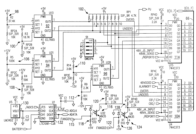
FIGURE 4 illustrates a schematic of the preferred
components of malfunction detection board 46 for
performing the functions of voltage monitoring for three
different voltage levels, temperature sensing, and
detection circuitry for monitoring the status of fans 52
and 53, discussed above in connection with FIGURE 1.
Specifically, FIGURE 4 illustrates three comparator
circuits 92, 94 and 96. Comparator circuits 92, 94 and
96 in the preferred embodiment are IC77665 chips, and
monitor the voltage levels of +5 VDC, +12 VDC and -12
TEX822/4-9 ~iJ~L~ 9 PATENT APPLICATION
VDC, respectively. ~or example, in connection with
monitoring the +5 VDC voltage level, a first voltage
divider 98 i8 connected between the supplied level of
+5 VDC and ground. The voltage~ divided by divider 98 is
connected to a ~irst SET input of comparator circuit 92.
Similarly, a second voltage divider 100 iB connected
between the supplied level of +5 VDC and ground, and the
divided voltage i5 connected to the second SET input of
comparator circuit 92. In the preferred embodiment,
first divider 98 has two resistors, the first having a
resistance of 37,400 ohms and the second having a
resistance of 10,000 ohms. Second divider 100 has two
- resistors, the first having a resistance of 18,700 ohms
and the second having a resistance of 10,000 ohms.
As is known in the art, the ICL7665 chip used for
comparator circuit 92 will provide two output signals.
The state at the first output, OUTl, indicates whether
the input voltage at input SETl is over a predetermined
threshold and, similarly, the state at the second output,
OUT2, indicates whether the voltage at the second input,
SET2, is below the predetermined threshold. The value of
the resistors in voltage dividers 98 and 100 affect the
magnitude of the input voltage relative to the absolute
value of +5 VDC. In the preferred embodiment, the
resistors of divider 98 are chosen so that a comparison
is made to determine if the +5 VDC supply exceeds its
nominal amount by 25% (i.e., exceeds 6.25 VDC).
Similarly, the resistors of divider 100 are chosen so
that a comparison is made to determine if the +5 VDC
supply falls below its nominal value minus 25% (i.e.,
below 3.75 VDC). As a result, for purposes of signal
identification, the outputs at OUTl and OUT2 of chip 92
are designated as OVER5 and UNDER5, respectively, for
indicating that the monitored voltage has risen above or
below a 25~ margin relative to the +5 VDC input value,
respectively.
TEX822/4-9 2 ~ ~ 3 ~ PATENT APPLICATION
Outputs OUTl and OUT2 are both connected to
respective pull-up resistors 102. In the preferred
embodiment, pull-up resistors 102 are part of a single
in-line package of nine resistors (labeled "SIP 9Rn).
Pull-up resistors 102 also provide a separate pull-up
signal (denoted PU) for purposes of providing a pull-up
voltage for other instances which may be needed within
the circuitry of malfunction detection board 46.
Output signals OUTl and OUT2 of comparator circuit
92 are connected to the inputs of a port circuit 104.
Port circuit 104, in the preferred embodiment, is a
74HC373 latch. Port circuit 104 is the second port
(i.e., of PORTO and PORTl) of the two read ports
discussed above in connection with reading and writing
from data bus 66. Thus, the eight outputs of port circuit
104 are connected in parallel to data bus 66. These
outputs are constantly latching their inputs because
their enable input pin (labeled G) is connected to VCC.
For purpose of outputting data to data bus 66, port
circuit 104 receives the /RDPORTl signal which is
presented by decoder 74, discussed above in connection
with FIGURE 3. Thus, upon assertion of the /RDPORTl
signal, the data latched by port circuit 104 is presented
to data bus 66.
Comparator circuits 94 and 96 are configured in a
similar manner as that of comparator circuit 92.
Accordingly, comparator circuit 94 has its SETl and SET2
inputs connected to voltage dividers 106 and 108,
respectively. Similarly, comparator circuit 96 has its
SETl and SET2 inputs connected to voltage dividers 110
and 112, respectively, Each of comparator circuits 94
and 96 have two output signals, OU~l and OUT2, both
corresponding to respective indications of whether the
input monitored signals either exceed or fall below a
predetermined threshold. For comparator 94, its two
output signals are connected to a 74HC373 port circuit
TEX822/4-9 ~ PATENT APPLICATION
114 ~n the same manner as comparator circuit 92 i8
connected to port circuit 104. Port 114 provides the
identical function of port circuit 104, but operates as
the first port (i.e., PORT0) for presentation of parallel
data to data bus 66. Further, port circuit 114 also
receives its enabling signal, /RDPORT0, from decoder 74.
The two output signals, OUTl and OUT2, of comparator
circuit 96 are also connected to inputs of port circuit
114 for presentation to data bus 66. In operation,
comparator circuits 94 and 96 operate in exactly the same
manner as comparator circuit 92, except comparator
circuit 94 makes the determination of whether the
supplied DC voltage level of +12 VDC either exceeds or
falls below 25% of a nominal +12 VDC level, while
comparator circuit 96 determines whether the input supply
voltage of -12 VDC exceeds or falls below 25% of the
nominal voltage level of -12 VDC.
FIGURE 4 further includes the circuitry for
monitoring the operation of fans 52 and 53, discussed
above in connection with FIGURE 1. As discussed above,
the preferred fans used to circulate air through the
chassis of computer 10 each include a mechanism for
indicating that the fan is operational. In the preferred
embodiment, this mechanism comprises a digital signal
level described as the signal "FANGO". Thus, each of the
two fans provides a respective FANGO signal, denoted as
FANGOl and FANG02. As illustrated in FIGURE 4, the
signal FANGOl is connected to the anode 115 of a diode
within an opto-isolator circuit 116. As is known in the
art, opto-isolator 116 includes a light-emitting diode
which, when activated, emits light upon a photo-
transistor, thereby causing the transistor to conduct.
The anode of the diode within opto-isolator 116 is also
connected through a resistor to +5 VDC. The collector of
the photo-transistor within the opto-isolator is likewise
connected through a resistor to +5 VDC. The collector of
TEX822~4-9 ~ 9 PATENT APPLICATION
28
the photo-transistor within the opto-isolator 116 is al~o
connected to a data input of port circuit 114 for
presentation to data bus 66.
The operation of the fan detection circuit i8 as
follows. Under normal operating conditions, the signal
FANGOl is low and, therefore, a 0-volt signal is placed
at anode 115 of the diode within opto-isolator 116. As a
result, the photo-transistor within opto-isolator 116 is
turned off. If, however, the fan associated with signal
FANGOl should become dysfunctional, then signal FANGOl
goes high, thereby permittir.g current to flow through the
diode of opto-isolator 116. Once the diode conducts, it
emits photons, thereby causing the photo-transistor of
opto-isolator 116 also to conduct. Once the transistor
conducts, its collector is connected to ground. This
change in state is communicated to port circuit 114 for
presentation to data bus 66 and detection by
microprocessor 62.
As stated above in the preferred embodiment,
computer 10 includes two fans and, therefore, the
schematic of FIGURE 4 illustrates a second and identical
fan monitoring circuit. Thus, a second signal FANGO2 is
provided to an anode 122 of the diode within an opto-
isolator 124. Further, anode 122 is connected through a
resistor 126 to a +5 VDC level. Similarly, the collector
of the photo-transistor within opto-isolator 124 is also
connected through a resistor 128 to a level +5 VDC. The
collector of the photo-transistor within opto-isolator
124 is connected to a data input of port circuit 104 for
purposes of presentation to data bus 66. The operation
of the second fan monitoring circuit is identical to that
of the first with the sole exception that its function is
to monitor a fan independent of the first fan monitored
by the first fan monitoring circuit. With respect to
both detection circuits, however, it should be noted that
the particular selection of opto-isolators is highly
TEX822/4-9 ~ PATENT APPLICATION
29
advantageous because they translate voltage from analog
to TTL levels, and also isolate! the analog voltage level
from the remainder of the digital circuit should an
analog voltage error occur.
FIGURE 4 further illustrates the schematic circuitry
implemented in the preferred embodiment for performing a
temperature sensing function. In particular, a
temperature sensor 130 is provided for producing an
electrical signal, VOUT, which is directly proportional
to the ambient temperature exposed to sensor 130. In the
preferred embodiment, temperature sensor 130 i8 an LM34DZ
temperature-controlled analog voltage circuit. The
output voltage, VOUT, i6 connected to a first channel
input, CHO, of an A-to-D converter 132. A-to-D converter
132, in the preferred embodiment, is an LTC1091-CJ8
serial A-to-D converter. The converter provides a serial
data output, denoted ADATA, which is connected to port 1
of microprocessor 62 (see FIGURE 4). The clock input of
A-to-D converter 132 receives a clock signal, denoted
ADCLK, from port 1 of microprocessor 62. Microprocessor
62 also provides an active low channel select signal,
/ADCS, from its port 1 to the channel select input, /CS,
of converter 132.
The operation of the temperature sensing function is
as follows. Temperature sensor 130 produces an analog
output voltage in response to its immediately surrounding
ambient temperature. Microprocessor 62 then activates
its A-to-D chip select signal, /ADCS, to enable converter
132. Further, microprocessor 62 sends a bit stream of
command code via signal ADATA to A-to-D converter 132.
This command code includes a command which instructs
A-to-D converter 132 to read the analog voltage at its
channel O ti.e., CHO) input. Accordingly, this selection
causes the analog voltage representing temperature to be
converted by A-to-D converter 132 into an 10-bit digital
representation. In the preferred embodiment, however,
TEX822/4-9 PATENT APPLICATION
A-to-D converter 132 is serial in operation and,
therefore, must be repetitively clocked in order to
extract each of its 10-bits of .Lnformation. As a result,
microprocessor 62 clocks conver1er 132 through signal
ADCLK so that each of the 10-bits are extracted and
presented as data to microprocessor 62 for purposes of
determining the temperature internal to computer 10. It
should be noted that a serial converter consumes
considerably less space on malfunction detection board 46
than would a parallel counterpart.
Microprocessor 62 utilizes the temperature
information to present an indication to the user or
monitor of computer 10 of any abnormal operating
temperature. Specifically, in the preferred embodiment,
the operating temperature within computer 10 should be
from 40 degrees Fahrenheit to 100 degrees Fahrenheit.
Thus, when the temperature deviates from this range,
microprocessor transmits a warning message to connector
86 (see FIGURE 3) for presentation to a remote console or
the like. Further, this condition is reset when the
temperature stabilizes between 45 degrees Fahrenheit and
95 degrees Fahrenheit. It should also be noted that this
detection of temperature deviation does not affect any
other monitoring function of malfunction detection board
46.
A-to-D converter 132 is further utilized in order to
monitor the vitality of the battery associated with
computer 10. Specifically, recall in connection with
FIGURE 2 that in the preferred embodiment, a rechargeable
battery backup system is implemented in order to operate
computer 10 in the instance that its normal -48 VDC
supply is interrupted. The output voltage provided by
this battery, denoted as BATTERY, is connected to a
second channel input, CHl, of A-to-D converter 132. As a
result, microprocessor 62 may assert /ADCS to enable
A-to-D converter 132. Again, microprocessor 62 sends
TEX822/4-9 2 ~ ~ 8 i~ ~ ~J PATENT APPLICATION
command code via signal ADATA to instruct converter 132
to select its CHl input, thereby inputting the battery
voltage into converter 132. Thus, A-to-D converter 132
al60 i operable to provide a digital representation of
the value of the battery voltage. This digital
representation is clocked out of converter 132 in the
same manner as is the temperature information converted
from temperature sensor 130. Further, once the digital
representation is made available to microprocessor 62, it
may be monitored in order to present a warning or
indication to a user of computer 10 should the battery
level fall below a desirable value.
FIGURE 5 illustrates a schematic of various
components from malfunction detection board 46, including
the preferred circuitry for connecting and driving an LED
display, a series of output ports from data bus 66 and
circuitry for providing contacts to a remote station for
both indicating the detection of a particular malfunction
and resetting computer 10. Specifically, FIGURE 5
includes three output port chips 134, 136 and 138, each
coupled to data bus 66, thereby defining write port 0,
port 1 and port 2. In the preferred embodiment, each of
port chips 134, 136 and 138 is a 74HC377 data latching
chip. Each of chips 134, 136 and 138 includes eight
parallel inputs for driving eight parallel output
signals. Each of output port chips 134, 136 and 138
receives a corresponding input latching signal, /WRPORT0,
/WRPORTl and /WRPORT2, respectively, from decoder 72. As
is known for a 74HC377, its clock pin is qualified by its
latching pin; that is, the latching pin (i.e., /G) must
be asserted in order for the chip to respond to a clock
signal. Thus, once a particular output port is enabled,
clocking the respective port will cause the respective
data signals illustrated in FIGURE 5 to be presented at
the port's output bits (i.e., Q0-Q7).
TEX822/4-9 PATENT APPLICATION
FIGURE 5 further includes a connector device 140 for
providing ~ignals to drive the LEDs on test/indicator
panel 28. In the preferred embodiment, connector 140 is
a 2x12 header device having its pins connected to the
signals illustrated in FIGURE 5. Thus, it should be
appreciated that a compatible connector and cable may be
coupled to connector 140 in order to drive the LEDs in
response to their corresponding signals. Further, a
review of the signals illustrated on the pins of
connector 140 reveals numerous signals in addition to
those necessary to drive indicators 30-40. These
additional signals are provided for user definition and
to accommodate a greater number of indicator~, if
desirable. For example, pin 22 of connector 140 provides
a signal labeled CRITICAL ~derived from pin 2 of port
circuit 138). A user may define a particular malfunction
as corresponding to this signal and, therefore, detection
of the malfunction will cause the CRITICAL signal to go
active. Once active, port circuit 138 may be written,
thereby causing the signal to be transferred via
connector 140 to a corresponding indicator.
As discussed above, the preferred embodiment of
computer 10 provides a series of contact terminal pairs
which may be accessed by a remote station such that the
remote station is notified that a system malfunction has
been detected. FIGURE 5 illustrates the preferred
ætructure for providing this feature. In particular, an
external connector 142 is provided having contacts which,
when monitored, provide an indication that a system
malfunction has occurred. In the preferred embodiment,
external connector 142 is a DB15 male connector. Of the
fifteen pins available on connector 142, ten of the pins
provide external malfunction indications. Each pair of
the ten detection pins provides a pair of contacts which
may be accessed by a remote user in order to indicate the
status of a particular aspect of system operation. As
~3~
TEX822/4-9 PATENT APPLICATION
set forth above, port circuit 1:18 provides variou~ type~
of generically labeled fault detection signals which may
be user-defined and transferred via connector 140 to
indicators. Port circuits 134 and 136 provide additional
similar signals. In addition to biasing connector 140,
some of these user-definable signals are used to control
the status between each pair of detection pins.
In particular, each pair of the signal indication
pins is connected to a respective one of a group of
relays 144, 146, 148, 150 and 152. Thus, for example,
pins 1 and 2, which provide two terminals corresponding
to a CRITALRM and a CRITALRMRET, are coupled to contacts
of a relay 144. Relay 144 is switched when the signal
CRITICALALARM (pin 5 of port circuit 136) is activated.
Thus, again, a user-definable event controls an action,
namely, a triggering of relay 144. Once relay 144 i8
triggered, it switches the status between pins 1 and 2
from either closed to opened or opened to closed.
Accordingly, a change in this status is an indication to
the remote station that the user-defined malfunction
corresponding to the pair of pins has occurred.
As another feature, relay 144 provides three output
terminals labeled Cl (i.e., commonl), NCl (i.e., normally
closed 1) and NOl (i.e., normally opened 1). Common
terminal Cl is connected to a first data output line 155
of relay 144. The latter two terminals are described in
terms of their function and, therefore, one is normally
closed with respect to the common terminal, Cl, when the
relay is deactivated, and one i8 normally opened when the
relay is deactivated (again, with respect to the common
terminal, Cl). In the preferred embodiment, normally
closed and normally opened terminals are connected to a
three-pin jumper 154. Jumper 154 has three pins, two of
which at a time may be connected to a second data output
line 156. Thus, it may be appreciated that a user may,
by selecting two of the three pins on jumper 154, connect
TEX822/4-9 ~ PATENT ~PPLICATION
34
output l~ne 156 to either the normally closed or normally
opened output of relay 144. Thus, ~or example, if a user
places a ~umper connector between the top two illustrated
pins of jumper 154, then output line 156 is tied to the
normally closed terminal of relay 144. As a result, when
operation of the overall computer is normal, then the
connection between output lines 155 and 156 is normally
closed and, thus, pin~ 1 and 2 of connector 142 are also
connected to one another. If, however, a critical alarm
signal were received by power driver 158, then relay 144
would switch, thereby opening the connection between
outputs 155 and 156. It should further be appreciated
that a user may alternatively place a jumper connector
around the lower two pins of jumper 154, thereby causing
output line 156 to be coupled to the normally opened
output, NOl, of~relay 144.
Relay 144 is driven by a power driver circuit 158.
In the preferred embodiment, power driver circuit 158 is
a two-input MC1472 chip. The MC1472 chip has two inputs
designated lB and 2B, and two respective outputs
designated lY and 2Y. Upon receipt of an input signal,
driver circuit 158 enables (active low) its respective
output. In the instance of chip 158, inputs lB and 2B
are connected to the CRITICALALARM and PWRLAMP signals,
respectively. As a result, outputs lY and 2Y are enabled
low when signal CRITICALALARM or PWRLAMP goes high,
respectively. Output lY is connected to the PWR- input
of relay 144. Thus, it may be appreciated that once the
CRITICALALARM signal is activated, the output lY of chip
158 goes low, thereby triggering relay 144 to change
state.
Chip 158 has its second input, 2B, connected to
receive the PWRLAMP signal which is provided by
microprocessor 62 through pin 16 of output port 136. The
corresponding output, 2Y, is connected to provide an
active low lamp signal, LAMPON/. The LAMPON/ signal is
TEX822/4-9 ~ PATENT APPLICATION
used to drive the input power indicator 56 discussed in
connection with FIGURE 2 above. Thus, in operation,
activation by microprocessor 62 of the PWRLAMP signal
causes chip 158 to activate its corresponding output,
LAMPON/, thereby illuminating indicator 56.
Relays 146, 148, 150 and 152 are configured in a
similar manner as relay 144. As a result, each of these
relays includes a respective jumper 160, 162, 164 and 166
connected between its respective normally closed and
normally opened outputs. Each of the common outputs of
these relays is connected to a respective data output
line 167, 169, 171 and 173. Moreover, the common pins of
- jumpers 160, 162, 164 and 166 are also coupled to
respective data output lines 168, 170, 172 and 174.
Thus, depending on the particular selection of a ~umper
connector, each of jumpers 160, 162, 164 and 166 may be
configured so that either the normally closed or normally
open relay output is connected to its respective data
output line 168, 170, 172 and 174.
Each of relays 146, 148, 150 ar.d 152 have their PWR-
inputs connected to an output of a corresponding power
driver circuit 176 or 178. Power driver circuits 176 and
178, in the preferred embodiment, are the same as power
driver circuit 158 and, therefore, are MC1472 chips. As
stated above, these chips provide two inputs and two
corresponding outputs. As a result, one of each of the
outputs of power driver circuit 176 are connected to the
PWR- inputs of relays 146 and 148, respectively.
Similarly, the two independent outputs of power driver
circuit 178 are connected to the PWR- inputs of relays
150 and 152, respectively. The two independent and
corresponding inputs of power driver circuit 176 are
connected to receive signals AUDIBLEALARM and FUSE,
respectively. Similarly, the independent inputs of power
driver circuit 178 are connected to receive signals
MAJORALARM and MINORALARM, respectively. Each of these
TEX822/4-9 ~ 6 ~ PATENT APPLICATION
actuating signals are user-definable to correspond to the
detection by microprocessor 62 of a particular
event/malfunction.
Power driver circuits 176 and 178 operate in the
same manner as power driver circuit 158. Accordingly, as
an example, power driver circuit 176 activates low either
of its outputs in response to either of its corresponding
inputs going high. For example, if the AUDIBLEALARM
signal is activated at input lB of chip 176, then output
lY is activated low. This active low output signal i5
input to relay 146, thereby causing relay 146 to change
state. As a result, the state of the normally closed and
normally opened outputs of relay 146 changes and, in
accordance with the placement of a jumper connection on
jumper 160, data output line 168 is either connected to,
or opened from, the other data output line 167.
FIGURE 5 further illustrates the preferred circuitry
for implementing the remote station external reset
feature discussed above. In particular, connector 142
- 20 includes two pair of pins labeled EXTRESETl and
EXTRESETlRET, as well as EXTRESET2 and EXTRESET2RET.
These signals correspond to the ability of malfunction
detection board 46 to reset the operation of computer 10
in response to a remote station's indication requesting
the computer to be reset. The first pair of external
reset signals are connected to pins 11 and 12 of
connector 142. Similarly, the second pair of external
reset signals are connected to pins 13 and 14 of
connector 142. The EXTRESETl signal is connected to the
anode of the diode within an opto-isolator 180. The
EXTRESETlRET signal is connected to the cathode of the
diode within opto-isolator 180. Similarly, the
EXTRESET2 signal is connected to the anode of the diode
within an opto-isolator 182 while the EXTRESET2RET signal
is connected to the cathode of the diode within opto-
isolator 182. The collector of the photo-transistor
2~
TEX822/4-9 PATENT APPLIcATION
within opto-isolator 180 i8 connected to the collector of
the photo-transistor within opto-isolator 182, and either
collector is capable of providing the EXTRST/ signal.
The emitters of the photo-transistors within opto-
isolators 180 and 182 are both connected to ground.
Further, the collectors of the photo-transistors within
opto-isolators 180 and 182 are connected through a
resistor 184 to the positive power supply voltage, VCC.
The operation of opto-isolators 180 and 182 i~ as
follows. In the example of opto-isolator 180, a remote
user having access to pins 11 and 12 may externally reset
computer 10 by forward biasing pin 11 with respect to pin
12. This forward biasing voltage causes the diode within
opto-isolator 180 to emit radiation upon its transistor,
thereby causing the transistor to conduct. Once
conducting, the transistor within opto-isolator 180 sinks
the current through resistor 184, thereby bringing signal
EXTRST/ low. Thus, it may be appreciated that the
forward biasing effect acts as a request to activate
signal EXTRST/ which is an active low indication that an
external request has been made. As discussed in
reference to FIGURE 3, the EXTRST/ signal is connected to
AND gate 80 and, through opsration of circuit 82, may
cause microprocessor 62 to be reset.
Opto-isolator 182 operates in the same manner as
opto-isolator 180. Thus, a remote user may provide a
forward bias voltage between pins 13 and 14 of connector
142, thereby forward biasing opto-isolator 182 and
causing its internal transistor to conduct. Once again,
this conduction causes current to flow through its
respective resistor 184 and pull signal EXTRST/ low.
FIGURE 5 further illustrates a pair of jumpers 186
and 188 for connecting to the terminals of fans 52 and
53, discussed abo~e. As described above, in the
preferred embodiment, fans 52 and 53 each have three-
input terminals for receiving a biasing voltage, a ground
TEX822/4-9 ~ 3 1~ ~ PATENT APPLICATION
38
and providing an operational signal, designated as FANGO.
Accordingly, jumper connector :L86 may be connected to the
terminals of fan 52 so that a +12 VDC biasing voltage i8
provided between pins 2 and 1 of ~umper connector 186,
while the FANGO signal is returned via pin 3 of connector
186. Jumper connector 188 is configured in an identical
manner as jumper connector 186 and, therefore, provides a
+12 VDC biasing voltage between pins 2 and 1 and receives
the operational FANGO signal on pin 3.
FIGURE 5 further illustrates the preferred circuitry
for driving two speakers which may be placed within the
housing of computer 10. Specifically, a power driver
circuit 190 receives at its input both a speaker signal
and a tone signal. In the preferred embodiment, power
driver circuit 190 is a MC1472 chip. The first output,
lY, of power driver 190 is connected to the PWR- input of
a relay 192. The second output, 2Y, of power driver
circuit 190 is connected to the second normally opened
output of relay 192. The first and second channel
outputs of relay 192 are connected to a speaker connector
194 for coupling to a first speaker. Similarly, the
normally closed outputs of both channel 1 and 2 of relay
192 are connected to second speaker connector 196 for
coupling to a second speaker. In operation, power
driver circuit 190 and relay 192 operate to provide
signals to the speakers which create audible sounds from
the speakers. Specifically, when a tone is desired, the
SPEAXER signal i8 kept high while the TONE signal is
oscillated. The frequency of oscillation of the TONE
signal causes a corresponding frequency of outputs from
relay 192. Consequently, the oscillating TONE signal
causes a speaker tone proportional to the frequency of
oscillation.
FIGURE 6 illustrates a schematic of certain
components of malfunction detection board 46, including
those preferably used in performing the functions of
TEX822/4-9 ~ 6 ~ PATENT APPLICATION
receiving various voltage leve]Ls, battery recharging, and
one mechanism of microprocessor resetting and power
conversion. Specifically, FIGI~E 6 includes a connector
198 for receiving various voltage levels from locations
external from malfunction detection board 46. In the
preferred embodiment, connector 198 is an 18-pin
connector. Connector 198 receives signals CBl/ and CB2/
on pins 15 and 16, respectively. These signals represent
the return reference levels for the two -48 VDC supply
voltages before they have passed through their respective
circuit breakers, discussed above.
Connector 198 also receives signal 48VGOOD on pin 8.
As described below, this 48VGOOD signal indicates that at
least one of the two post-circuit breaker voltages, -48VA
or -48VB, is active. The specific generation of signal
48VGOOD is illustrated in connection with FIGURE 9,
below. Connector 198 also receives the POWERGOOD signal
on pin 6. The POWERGOOD signal is an indication from the
power supply board that it is receiving sufficient supply
voltage. Thus, if the signal is inactive, there is
insufficient supply voltage to the power supply board.
Finally, connector 198 receives signals 48VA SENSE and
48VB SENSE which are connected to pins 18 and 17,
respectively. These two signals are digital signals
representing the -48 VDC supply voltages before they pass
through their respective circuit breakers (i.e., CBl and
CB2). Specifically, these two signals are digital level
signals which represent that their corresponding pre-
circuit breaker signal is active (i.e., whether the
-48 VDC is present before the circuit breaker). Thus, if
either signal goes inactive, there is an indication that
the corresponding power supply voltage has been
discontinued before its respective circuit breaker.
The +5 VDC, +12 VDC and -12 VDC voltage levels are
connected to various pins on connector 198, as
illustrated in FIGURE 6. In addition, signals CBl/,
7~'J~
TEX822/4-9 ~ PATENT ~PPLICATION
CB2/, 48VGOOD and POWERGOOD are each connected through
respective pull-up resistors to VCC.
- FIGURE 6 further includes a voltage divider 200
which is connected to the backup battery supply voltage,
VBAT. In the preferred embodiment, voltage divider 200
has a first resistor connected between the battery
voltage VBAT and a digital signal, BATTERY. A second
resistor 204 is connected between the signal BATTERY and
ground. In the preferred embodiment, resistor 202 is a
1010,000 ohm resistor and resistor 204 is a 22,000 ohm
resistor. The divided battery voltage, BATTERY, is
connected to the second channel input, CHl, of A-to-D
converter 132 discussed in connection with FIGURE 4.
Thus, as discussed above, this voltage may be reviewed by
microprocessor 62 to determine the vitality of the
battery backup system.
FIGURE 6 also illustrates a battery recharge chip
206. In the preferred embodiment, battery recharge chip
206 is a UC3906 chip. Battery recharge chip 206 is part
of an overall battery recharge circuit, designated
generally at 208. Battery recharge circuit 208 is
constructed according to principles known in the art and
provides a reference node 210 and a ground 212. The
rechargeable battery discussed above in connection with
FIGURE 2 has its positive and negative terminals
connected between nodes 210 and 212, respectively.
Moreover, circuit 208 operates to continuously recharge
the battery connected between nodes 210 and 212 during
normal operation of computer 10. As a result, the
battery remains fully charged in the instance that it is
necessary to supply power to computer 10 should both of
the normally operating -48 VDC power supplies fail.
FIGURE 6 also illustrates a connector 214 for
connecting/disconnecting power supply voltages to
motherboard structure 44, discussed above. In the
preferred embodiment, connector 214 comprises a 12-pin
TEX822/4-3 ~ PATENT APPLICATION
` 41
connector which is mateable wi1:h a connector and cable
for connecting to motherboard structure 44. Pins 1, 2,
and 7 of connector 214 are connected to +5 VDC. Pins 3,
i, 9 and 10 of connector 214 are connected to ground.
Pins 5 and 11 of connector 214 are connected to +12 VDC.
Pin 12 of connector 214 is connected to -12 VDC.
Pin 6 of connector 214 i8 connected to the output of
an AND gate 216. AND gate 216 has its inputs connected
to the POWERGOOD signal (from the power supply board) and
the RESETSPARC signal (from pin 9 of port circuit 138).
Under normal operating conditions, the POWERGOOD signal
is high and the RESETSPARC signal is high. Accordingly,
the output of AND gate 216 is high. If, however, a
situation arises in which it is desirable to reset the
SPARC microprocessor on motherboard 44, then the
RESETSPARC signal is toggled from high to low. This low
signal is then combined with the high POWERGOOD signal by
AND gate 216, thereby producing a low output which may be
interpreted by the SPARC microprocessor through pin 6 of
connector 214.
FIGURE 6 further illustrates the preferred power
conversion circuitry 218 of the present invention. Power
conversion circuitry 218 is constructed according to
principles known in the art, using the various components
as illustrated. Power conversion circuitry 218
ultimately provides a potential in an output node 220,
the potential equal to VCC. It should be noted that the
VCC potential at output 220 provides the VCC bias for all
other VCC potentials illustrated in FIGUREs 3-9.
Further, from FIGURE 6, it should be appreciated that the
VCC potential is backed up by VBAT, the battery backup
voltage, at a node 222. Thus, if the regular supply to
power conversion circuitry 218 of +5 VDC fails, then VBAT
is able to drive circuitry 218 so that VCC ~ontinues to
be supplied. Thus, the various components of FIGUREs 3-9
TEX822/4- 9 2 ~ PATENT APPLICATION
42
powered by VCC are supported by the battery backup
feature.
FIGURE 7 illustrates a schematic of various
capacitor configurations used in the preferred embodiment
of the present invention. Spec:ifically, a fir6t
capacitor network 228 is provicled and is connected
between VCC and ground. In the preferred embodiment,
capacitor network 228 has sixteen 0.0~ microfarad
capacitors connected in parallel. FIGURE 7 further
illustrates three additional capacitor networks 230j 232
and 234. Capacitor network 230 i8 connected between
+5 VDC and ground and has two capacitors connected in
parallel, one of a value of 0.01 microfarads and the
other of a value of 22 microfarad6. Capacitor network
232 is connected between +12 VDC and ground and includes
three capacitors, those capacitors having values of 0.01
microfarads, 0.01 microfarads and 22 microfarads.
Finally, capacitor network 234 is connected between
-12 VDC and ground and is a single 22 microfarad
capacitor. Each of capacitor networks 230, 232 and 234
provides the function of stabilizing power supply during
supply fluctuations. In addition, networks 230 and 232
help to substantially reduce the amount of noi6e which
may otherwise exist on the +5 VDC and +12 VDC voltage
supply levels.
FIGURE 8 illustrates a perspective view of the board
layout for malfunction detection board 46 which has been
discussed generally above in connection with FIGURE6 1
and 2 and schematically in connection with FIGUREs 3-7.
The component part designations illustrated in FIGUREs
3-7 are carried forward in FIGURE 8. As a result, if a
malfunction occurs within the board (or the power supply
immediately below the board), then it may be quickly
replaced with a new board so that the overall downtime of
computer 10 is minimized.
""~ ~, 9
TEX8 2 2/ 4 -9 PATENT APPLICATION
43
Malfunction detection board 46 iB illustrated as
having a front end 236 and a rear end 238. Front end 236
i8 disposed within computer 10 toward its front panel 12
and, therefore, lies immediately behind test/indicator
panel 28. Rear end 238 of malfunction detection board 46
is disposed toward rear panel 18 of computer 10, and
further lies within rear housing 50. From FIGURE 8,
therefore, it may be appreciated that the complete
functionality of malfunction detection board 46 is
performed, in the preferred embodiment, on a single
integrated board which may be easily disposed within
computer 10. Because the board iB an integral unit, it
may be easily removed and replaced within computer 10.
Further, and is discussed in greater detail above, the
removal of rear housing 50 and its movement away from the
rear of computer 10 causes malfunction detection board 46
to be pulled away from computer 10 for easy replacement
purposes. Having pulled malfunction detection board 46
away from the remainder of computer 10, only a few cables
need be disconnected from malfunction detection board 46
in order to fully remove it and replace it within
computer 10.
FIGURE 9 illustrates a schematic of an interface
board designated generally at 240. Interface board 240
is preferably constructed as a separate board from the
power supply board and malfunction detection board 46,
and acts primarily as a ~unction for cabling between the
power supply board, the malfunction detection board, and
the actual power supply signals. In the preferred
embodiment, interface board 240 is disposed vertically in
housing 50 and adjacent rear end 238 of malfunction
detection board 46. As a result, interface board 240 may
be easily and quickly accessed for
connection/disconnection in the event that housing 50 i8
removed from computer 10.
TEX822/4-9 2 ~ ~i 8 '1 ~ ~ PATENT APPLICATION
In the preferred embodiment, interface board 240
includes three connectors 242, 244 and 246. Connector
242 is preferably an 18-pin connector, and is for
connecting via a cable to connector 198 shown in FIGUR~
6. Connector 244 is preferably a 20-pin connector, and
is for connecting to various different locations within
computer 10, including the circuit breakers and input
- power indicator 56. Connector 246 is preferably a
fifteen position connector and may be coupled directly to
the power supply board.
Interface board 240 further includes two discrete
resistors 248 and 250. In the preferred embodiment, both
resistors 248 and 250 are 3.3 Kohm one-watt resistors.
Interface board 240 further includes two diodes 252 and
254. In addition, interface board 240 includes three
opto-isolators 256, 258 and 260.
Interface board 240 also includes two power supply
inputs 262 and 264 (labeled CBl and CB2, respectively)
which represent the -48 VDC supplies before their
respective circuit breakers. Input 262 is connected to
pin 20 of connector 244, as well as to the cathode of the
diode within opto-isolator 258. Similarly, input 264 is
connected to pin 19 of connector 244, as well as to the
cathode of the diode within opto-isolator 260. The
return reference levels for both CBl and CB2 are labeled
CBl/ and CB2/, respectively. Return level CBl/ is
connected to pin 8, and return level CB2/ is connected to
pin 9 of connector 244.
The anode of the diode within opto-isolator 258 is
connected through a resistor 266 to pin 14 of connector
244. Similarly, the anode of the diode within opto-
isolator 260 is connected through a resistor 268 to pin
14 of connector 244. In the preferred embodiment, both
resistors 266 and 268 are 8.2 Kohm, one-watt resistors.
The emitters of both photo-transistors within opto-
isolators 258 and 260 are connected to ground. The
TEX822/4-9 ~C~ PA~ENT APPLICATION
collector of the photo-transistor within opto-isolator
258 provides a digital signal, designated as 48VA SENSE,
which is connected to pin 18 of connector 242.
Similarly, the collector of the photo-transistor within
opto-isolator 260 provides a digital signal, designated
as 48VB_SENSE, which is connected to pin 17 of connector
242. Signals 48VA SENSE and 48VB_SENSE are digital
representations that the first and second power supply
voltages of -48 VDC, respectively, are present before
their corresponding circuit breakers, CB1-A and CB2-B.
Specifically, as indicated above, inputs 262 and 264
receive respective -48 VDC redundant power supply inputs
(i.e., CB1 and CB2) before the supplies are connected
through respective circuit breakers. Once the supplies
are attached, they are monitored as follows. In the
example of input 262, the first supply voltage i8
connected to the cathode of the diode within opto-
isolator 258. This connection causes the diode of opto-
isolator 258 to conduct, thereby causing its
corresponding transistor to conduct as well. As a
result, the output signal from opto-isolator 258,
48VA_SENSE, will change state. As discussed above, this
signal is sensed and, therefore, the change in state is
detectable. Likewise, input 264 receives the second
redundant voltage supply (denoted CB2) and, therefore,
the output of opto-isolator 260 presents a digital
representation (i.e., 48VB SENSE) of when the second
voltage supply is present before the circuit breaker.
Accordingly, microprocessor 62 can monitor the status of
these two signals to determine if either supply has
failed before the circuit breaker. Given this
determination, a user can be notified that a problem has
occurred in the supply which is external to computer 10.
As a result, the user can focus its troubleshooting
effort on the external supply without having to expend
TEX822/4-9 ~ )f~ PATENT APPLICATION
46
valuable time examining the operational vitality of
computer 10.
Connector 244, in general, receives the two -48 VDC
supply voltages after they have been passed through their
S respective circuit breakers. ~rhese voltage levels are
designated -48VA and -48VB. Specifically, pins 2, 3, and
12 of connector 244 receive -48VA, and pins 1, 10 and 11
of connector 244 receive -48VB. The return reference
level for both post-circuit breaker voltages -48VA and
-48VB is labeled -48RET. This return reference level,
-48RET, i8 connected to pins 4, 5, 13, 14 and lS of
connector 244. Each post circuit breaker supply voltage,
-48VA and -48VB, is connected to a respective cathode of
a diode 2S2 and 2S4. The anodes of diodes 252 and 2S4
are connected to pin 26 of connector 246 and provide a
common voltage signal labeled -48VCOM. ThiS
configuration creates a "diode OR" configuration whereby
the two post circuit breaker voltages are logically ORed
together such that the resulting voltage, -48VCOM, will
exist if either one of the post circuit breaker voltages,
-48VA or -48VB, exists. Thus, it should be appreciated
that diodes 2S2 and 2S4 are configured in manner to
provide a redundant system whereby an ultimate power
supply voltage, -48VCOM, will exist even if one of the
2S two post circuit breaker voltages, -48VA or -48VB, fails.
In addition, the anodes of diodes 2S2 and 2S4 are
connected to the cathode of the diode within an opto-
isolator 256. The anode of the diode within opto-
isolator 256 i8 connected to pins 4, 5, 13, 14, and 15 of
connector 244, which provide the return voltage, -48RET,
for the post-circuit breaXer -48 VDC power supplies.
Thus, it should be appreciated that in the instance that
either diode 2S2 or diode 254 provides a voltage for
-48VCOM, opto-isolator 256 is forward biased, thereby
causing its transistor to conduct. As a result, this
conduction causes a change in the digital state of the
TEX822/4-9 ,~,~ $~i~r1i~j3~l~ PATENT APPLICATION
output signal of opto-isolator 256, namely, 48V SENSE.
Thu~, it should be appreciated that signal 48VGOOD
presents a digital representation that at least one of
the two post circuit breaker voltages, -48VA or -48VB,
exists. This post circuit breaker voltage confirmation
signal, 48VGOOD, is connected to pin 8 of connector 242.
Accordingly, microprocessor 62 can monitor the status of
the signal at pin 8 of connector 242 to ensure that at
least one power supply voltage is vital after its
respective circuit breaker. Further, if signal VGOOD
fails while signals 48VA SENSE and 48VB_SENSE indicate
valid external power supply, then a user can be so
notified and focus its troubleshooting effort on the
circuit breaker(s) or other internal connections of
computer 10.
Connector 246, in general, is for connecting to the
power supply board. As discussed above in connection
with FIGURE 1, the power supply board is disposed
immediately below malfunction detection board 46 and is
integrally removable by retracting housing 50 from
computer 10. Once retracted, the power supply board may
be disconnected from connector 246, thereby providing
independent access to either board. Connector 246
provides the necessary 48-volt supply to the power supply
board and receives back from the board the necessary DC
voltage levels in order to drive the remainder of
circuitry associated with computer 10 as well as the PWR
GOOD signal discussed above. Thus, pin 26 of conneGtor
246 receives the diode OR voltage, -48VCOM, which is
active in the case that either -48 volt post-circuit
breaker voltage exists. Pin 24 of connector 246 is
connected to pins 4, 5, 13, 14 and 15 of connector 244
and, therefore, receives the -48 voltage return signal
labeled -48RET from connector 244. The remainder of the
pins of connector 246 provide return voltage levels
and/or signals from the power supply board.
TEX822/4-9 ~ ~i 3 '1~ ~ PATENT APPLICATION
48
Specifically, pins 4 and 6 of c:onnector 246 provide a
voltage level of +5 VDC. Pins 20 and 22 of connector 246
provide a voltage level of +12 VDC. Pins 16 of connector
246 provides a voltage level ol` -12 VDC. Pins 8, 10, 14
and 18 of connector 246 are connected to ground.
Finally, pin 12 of connector 246 provides a digital
signal labeled PWR GOOD which provides an indication by
the power supply board that the power supply board is
receiving its own supply voltage.
Connector 242 i5 for coupling to malfunction
detection board 46 in order to provide board 46 the
necessary voltage supply levels. In addition, connector
242 provides and receives certain digital signals
indicative of various functions so that microprocessor 62
may monitor the signals to respond to a detected
malfunction. Specifically, pins 1 and 2 of connector 242
are connected to pin 6 of connector 246 and, therefore,
receive a voltage level of ~5 VDC from the power supply
board. Pins 3 and 4 of connector 242 are connected to
pins 10 and 18 of connector 246 and, therefore, are
connected to ground. Pin 5 of connector 242 is connected
to pin 22 of connector 246 and therefore, receives a
voltage level of +12 VDC.
Pin 6 of connector 242 is connected to pin 12 of
connector 246 and, therefore, receives a digital signal,
PWR GOOD, discussed above. Pin 7 of connector 242 is
connected to pin 7 of connector 244 and provides a
signal, LAMPON/, to connector 244 to turn on input power
indicator 56. Specifically, the forward bias voltage for
input power indicator 56 is the signal LMP PWR which is
connected to pin 16 of connector 244, while the return is
the LAMPON/ signal from pin 7.
Pin 8 of connector 242 is connected to the collector
of the photo-transistor within opto-isolator 256 and,
therefore, receives a digital signal representing that
TEX822/4-9 ~ PATENT APPLICATION
either of the two post circuit breaker supply voltages is
active, namely, 48VGOOD.
Pin 9 of connector 242 is connected to pin 4 of
connector 246 and therefore, receives a supply voltage
level of +5 VDC. Pin 10 of cormector 242 is connected to
pin 16 of connector 244 and provides the LMP PWR for
enabling input power indicator 56. Pins 11 and 12 of
connector 242 are connected to pins 8 and 14,
respectively, of connector 246 and, therefore, are
connected to ground. Pin 13 of connector 242 i8
connected to pin 20 of connector 246 and, therefore,
receives a supply voltage of ~12 VDC. Pin 14 of
connector 242 is connected to pin 16 of connector 246
and, therefore, receives a power supply voltage -12 VDC.
Pins 15 and 16 of connector 242 are connected to
pins 8 and 9, respectively, of connector 244 and,
therefore, receive from connector 244 the return
references for power supply voltages, labeled CBl/ and
CB2/, before their respective circuit breakers. Finally,
pins 17 and 18 of connector 242 are connected to the
collectors of the photo-transistors within opto-isolators
268 and 258, respectively, and, therefore, provide
signals 48VB SENSE and 48VA SENSE.
From the above, one can appreciate that the present
invention provides various features and advantages over
previously existing computers. It should be noted,
however, that while the advantages of the present
invention have been described in detail, various changes,
substitutions and alterations can be made herein without
departing from the spirit of the invention. For example,
while computer 10 has been described as advantageous in
connection with the telecommunications industry, clearly
the inventive features described could have widespread
application to all types of computers, including those
used for personal use, business use and other industrial
applications. Further, while specific selected circuitry
TEX822/4-9 PATENT APPLICATION
; 50
has been described in connection with the preferred
embodiment, various types of alternative circuits could
be chosen by a person having ordinary skill in the art.
For example, many of the discrete components including
integrated circuits could be replaced with substitutions
or equivalent devices. As another example, certain
function~ or operations could be combined using an
application specific integrated circuit. Nonetheless,
the present invention contemplates such types of changes.
Still other examples too numerous to list also follow
from the previous description and in no way should depart
from the scope of the present invention as defined by the
following claims.