Note: Descriptions are shown in the official language in which they were submitted.
~'~ 9-1/0772 1 P~'J~CTS90/06612
INDUCTI':ELY COUPhED SAW DEVICE AND
METi-iJD FOR MAKING THE SAME
BACKGROUND OF THE INVENTION
The present invention relates to apparatus for coupling
electrical energy into and/or out of a surface acoustic wave
("SAW") device. More particularly, the present invention
relates to apparatus for coupling energy into and out of a
SAW device which serves as a transponder in a "passive
interrogator label system".
A "passive interrogator label system", so-called, is a
radar system utilizing transponders which are capable of
receiving an interrogating first signal, processing this
signal and transmitting a second signal, in reply, that is
derived from the first signal and contains encoded informa-
tion. Because the encoded information normally includes an
identification code that is unique to each transponder, and
because the transponders of such a system are relatively
light weight and small and may be easily attached to other
objects to be identified, these transponders are sometimes
referred to ws "labels". Furthermore, the transponders,
which may be implemented by SAW devices, carry no
self-contained power source, such as a battery, that must be
periodically replaced. Consequently, these transponders are
denamirzated as being "passive"; hence the name "passive
interrogator label system°'.
Passive interrogator label system of the type to which
the present invention relates are disclosed, for example, in
the following U.S. patentso
vv~ 9mo77~x P~r/us90/os6~x -
' 2 cr:, ;:1
U.S. Patent No. 4,737,789 of Paul S. Nysen for
''Inductive Antenna Coupling for a Surface Acoustic
Wave Transponder;
U.S. Patent No. 4,703,327 of Anthony J. Rosset-ti
and Paul A. Nysen for "Interrogator/Receiver
System for Use With a Remote Transponder"; and
U.S. Patent No. 4,737,790 of Halvor Skeie and
Donald Armstrong for "Passive Interrogator Label
System with a Surface Acoustic Wave Transponder
Operating at i.ts 'Third Harmonic and Having In-
creased Bandwidth°'.
In general, a passive interrogator label system in--
dudes an "interrogator" for transmitting a fir st radio
frequency signal; at least one passive ~transponder which
receives this first signal, processes it, and sends back a
second radio frequency signal containing encoded
information; and a receiver; normally located next to the
interrogator, for receiving the second signal and decoding
the transponder encoded information.
~~'~(~~~.~.~
dv0 91107782 3 f~f/~J~9010~61.~
for example, the antenna characteristics required for
'this application, operating at a frequency of approximately
915 MHz., determine that the antenna be physically approximately
one inch wide and three inches long. The SAW
device, to which the antenna is coupled, is also placed on
the substrate to form the complete assembly or "label".
This flat, card-like structure is ideal far many
applications such as identification badges far personnel and
ID tags for automobiles, factory parts or the like.
The aforementioned U.S. Patent No. 4,737,789 describes
means for inductively coupling a SAW transponder to an
antenna by means of an inductive loop farmed by at least one
turn of an electrical conductor and having an inductance
which is substantially equal to the capacitance presented at
the terminals of the SAW device within the frequency range
of operation. The two free ends o:~ the loop are
electrically connected to the two transducer terminals of
the SAW device so that the loop and the device form a
resonant circuit at the frequency range of operation.
The U.S. Patent No. 4,737,789 also describes a package
comprising a substrate formed by a Mylar sheet coated on
both sides with a polyethylene based, thermally activated
adhesive,~ a SAW device comprising a lithium niobate
piezoelectric substrate and a partial turn of a metal foil
inductive loop, bonded to the Mylar substrate and
electrically connected to the two terminals of the SAW
device. This entire assembly is then eneapsula~ed and
placed next to an inductive loop which is electrically
connected to or formed integrally with the antenna.
While the SAW device and its associated inductive loop,
so connected, may be conveniently packaged together in a
glass or aeramic.envelape to form a separate manufactured
~~~~~~3
'v~o 9~io»~~ ~ P~iu~~oe~s~g-._
unit, which may be .then mounted adjacent an antenna
structure, this package assembly necessari7.y requires
several manufacturing steps to produce. This package is
also relatively 'thick in its final form. Whereas the
physical size of assembly is not significant in many
applications, certain applications, such as wallet size ID
cards, require the assembly to be as thin as possible.
SUMMARY OF THE INVENTION
It is a principal object of the present invention to
provide a SAW device which may be inductively coupled to a
signal source or sink such as an antenna.
It is a further object of the present invention to
provide a SAW device of the above noted type which is
contained in an extremely small, thin and yet robust
package.
These objects, as well as ather objects which will
become apparent from the discussion that.follows, are
achieved, in accordance with the present invention, by
providing a SAW device having a conductive loop deposited on
the active surface of the piezoelectric substrate which is
electrically connected at its ends to the two transducer
terminals of the device. The conductive loop forms an .,
inductive element for ooupling enefgy into ani~ out of the
SAW device. The active surface containing the acoustic
piths of the SAW device is protected by a non-conductive
cover disposed above, and attached to, the surface by means
of an adhesive. This cover may be made of glass, for '
example,
CA 02068513 1998-03-12
This device, comprising the SAW substrate with the
inductive loop pattern and its associated cover is placed in a
protective frame which laterally surrounds the SAW substrate
and cover. The protective frame, which may be made of metal
to provide resilience, may have the same thickness as the
combined thickness of the substrate and cover. This entire
package, including the substrate cover and frame is therefore
extremely small in its dimensions and yet mechanically strong
and completely passivated and protected against outside
elements.
In one aspect, the invention resides in a surface
acoustic wave (SAW) device comprising:
(a) a SAW substrate having an exposed surface;
(b) at least one SAW transducer, disposed on said
surface of said substrate, for converting between electrical
energy and SAW energy that traverses said surface along at
least one acoustic path, said transducer having first and
second electrical terminals; and
(c) a first conductive, planar loop disposed on said
surface of said substrate and electrically connected at its
ends to said first and second terminals;
(d) a second conductive, planar loop disposed in
substantially plane parallel relationship with said first
loop, said second loop having third and fourth electrical
terminals, said first and second loops forming an inductive
element for coupling energy into and out of said SAW device
72003-11
CA 02068513 1998-03-12
5a
between said third and fourth terminals, on one hand, and said
first and second terminals, on the other.
In a further aspect, the invention resides in a
process of producing an encapsulated surface acoustic wave
(SAW) device comprising a SAW substrate having an exposed
surface and at least one SAW transducer, disposed on said
surface of said substrate, for converting between electrical
energy and SAW energy that traverses said surface along at
least one acoustic path, said transducer having first and
second electrical terminals; said process comprising the steps
of: (a) depositing, on said surface of said substrate, a
conductive partial loop, said loop being electrically
connected to said first and second terminals;(b) adhering a
non-conductive cover to said substrate above said surface in
the region of said acoustic path.
For a full understanding of the present invention,
reference should now be made to the following detailed
description of the preferred embodiment thereof, taken in
conjunction with the accompanying drawings.
72003-11
~0~~7~~
vvo 9mo~asz 6 P~/u~9o/OS~~~.:Y .
BRIEF.DESCRIPTIOI~T OF THF DRAWINGS
::
Figure 1 is a representational diagram of apparatus
according to the prior art for coupling a SAW device to an ..
antenna.
Figure 2 is a top view of a transponder according to
the prior art comprising a SAW device connected to a dipole
antenna formed of metal foil and bonded to a Mylar sheet.
Figure 3 is a cross-sectional view of a SAW device, as
disclosed in the prior art, connected to a metal foil
antenna and packaged within a small housing.
Figure 4 is a top-view of the SAW substrate surface
comprising a multitude of transducers connected to two bus
bars, a conductive loop connected to the bus bars, and a
multitude of reflectors and delay pads positioned along the
surface acoustic wave paths defined by the transducers.
Figure 5 is a top-view of a non-conductive cover for
the substrate of Figure 4.
Figure 5 is a cross-sectional view of a non-conductive
cover of Figure 5 disposed on the SAI9 substrate of Figure 4,
taken along the section line 6-6 in Figure 5.
Figure 7 is a perspective view of the SAW substrate and
cover of Figures ~-6 assembled together.
Figure 8(a) is a top-view ,ref the SAW device of Figure 7
arranged in registration with a dipole antenna to form a '
transponder.
P~f/lJS9i)/06612
!~O 9110778 7
Figure 8(b) is a top-view of a highlighted portion of
Figure 8(a) displaying the SAW device and inductive coupling
loop of the antenna in further detail.
Figure 8(c) is a cross-sectional view taken along the
line 8 (c) - 8 (c) in Figure 8 (b) .
Figure 9 is a top view of a SAW device disposed in
registration with an antenna.
Figures 10(a) through 10(c) are representational,
cross-sectional views showing the placement of a SAP;
substrate, an adhesive and a cover layer into a cavity
mold, and disposing a squeeze plate on top of the cover to
cause the adhesive to properly adhere to the substrate and
cover.
Figure 11 is a top-view of 'the cavity mold of Figure
10.
Figure 12 is a cross-sectional view of the cavity mold
of Figure 11, taken along the lines 12-12 thereof.
Figure 13 is a cross.-sectional view of a SAW device.
Figure 14 is a perspective view illustrating a SAW
device arranged. in a protective frame.
Figure 1~ is a top~view of the SAW device and
protective frame of Figure I4.
Figure 16 is a cross-sectional the SAW device and
protective frame taken along the line 16-~16 in Figure 15.
2~~8~~.~
1~'O 91107782 8 PCf/US~301~661,". ', ,
Figure 17 is a perspective view of a spring clamp
suitable for applya:ng pressure to a SAW device during
manufacture.
Figure 18 is a cross-sectional view of the spring clamp
of Figure I7 in a position to apply pressure.to the cover of
a SAW device.
i
eve ~~/o~~s2 9 ~ ~ ~ ~ ~ ~ ~~/u~~o/os~l2
DESCRIPTION OF TI3E PREFERRED EMBODIMENTS
The preferred embodiments of the present invention will
now be described with reference to Figures 1 through 18 of
the drawings. Identical elements in the various figures are
designated with the same reference numerals.
Figure 1 illustrates the basic configuration of a
passive interrogator label system, with induction
input/output coupling so described in the aforementioned
U.S. Patent No. 4,737,789. The design comprises a SAW
device having a conductive loop inductively coupled with an
antenna. Previously, a SAW device required direct wiring to
its dipole antenna, which 'this design eliminates.
An alternative, and direct means.for connection to
antenna is shown in Figure 2, whereby the SAW device is
connected to several contact pads by physically wiring both
together. A dipole antenna, which forms an inductive loop
or DC short, is incorporated to prevent the build-up of
static electricity.
Referring to Figure 3, (cross-sectional view of Figure
2), the SAW device is encapsulated in a bos.-like container
held together by an epaaty adhesive. This view illustrates
the necessity of connecting several leads to a contiguous
section to form a DC short between both antenna elements.
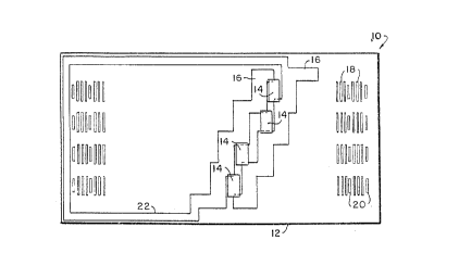
Figure 4 illustrates a device 10 having a substrate
layer 12 comprising a multitude of SAW transducers 14
positioned on the substrate layerl2 with respect fro a
multitude of xeflectors 20 and delay pads 18. Each SAW
transducer l4 has a pair of reflectors 20 positioned on both
sides and is adjoined to a conductive bus bar 16,
interconnecting each transducer 14. The conductive bus bars
~v~ 9no~~sz ~ ~ ~ ~ ~ ~. ~ 1 o p~~u~~oioss~.°..;a r
16 and transducers 14 may be farmed from the same conductive
material 22, i.e., aluminum. Connected to the bus bars is a
U--shaped conductive loop 22, having an approximate thickness w
of 4,000 Angstroms. The sub strate layer 12, upon which all
transducers 14 and conductive layers 16 and 22 are disposed,
is a piezo-electric material, preferably lithium niobate.
This configuration produces,a.conductive loop 22, which is
inductively coupled with a dipole antenna (not shown).
As is the case with most highly sensitive electronic
equipment, protection from foreign objects, be it dust
particles, fingers or possible shorts, is necessary for
consistent and proper operation. The first embodiment
discloses a protective means for SAt9 substrates which by
design, eliminates unwanted interference within the acoustic
path or paths in order to maintain proper SAW performance..
As shown in Figures 5, 6 and 7, a non-conductive cover
24 is disclosed, adjoined directly above the SAW substrate
layer 12 by means of an adhesive sheet 26. The
non-conductive cover 24 acts as a protective means for
the substrate surface 12 and maintains the substrate
surface's integrity. Figure 7 is a perspective view of the
SAW devace 28, encapsulated by the cover 24, substrate layer
12 and adhesive 26. The non-conductive cover should
comprise a thickness range of .003 to .030 inches, and may
be farmed from glass. $oth substrate 12 and non-conductive
cover 24 should comprise a lateral width dimension of 0.1 to
0.2 inches and a lateral length dimension of 0.2 to 0.4
inches. The epoacy adhesive 26 should comprise a thickness
range of .002 to :010 inches, and a width of .01 to .05
inches. A typical adhesive layer used is the 3M brand AF -
42 Film Adhesive for its strong adhesive properties~with
both glass and metal, and its.limited outgassing during ,
curing.
~'~ 91/07782 .~1 PC.°f/1JS90/~1b512
Figures 8 (a-c) and 9, illustrates how the SAtnT device
assembly of Fig. 7 must be placed in registration with an
inductive loop on an antenna to couple energy between the
antenna and the SAW device. Figure 8(a) illustrates a top
view of a SAW device 28 positioned at the center of dipole
antenna 30, formed of metal foil or conductive ink. The
antenna 30 is disposed on a flat substrate 32, which may
comprise polyethyline coated Mylar. The SAW devices
placement is further highlighted in Figure 8(b). The SAW
device 28 is placed in registration with a corresponding
loop area 34 on the antenna 30 to provide the inductive
coupling between the antenna and the conductive loop 22 on
the devices. A cross-sectional view of the relative
positioning and alignment of the SAW device 28 ~to precisely
register the conductive loop 22 with respect to the
inductive loop portion 24 of the antenna is shown in Figure
8 (c ) .
A second embodiment of the present invention discloses
a more complete package, illustrated in Figures 10(a-c).
initially, the substrate layer 12 is placed into a cavity
mold 40 as shown in Figures 10(a) and 11.. An adhesive sheet
26, as previously disclosed, is disposed on the substrate
layer 12 to form~SAW device 28. The configuration of
non-conductive cover and substrate layer allows for the
transfer of acoustic energy between transducer and
reflector, whale permitting for the direct protection of the
substrate's upper'surface. Furthermore, a squeeze-plate, is
then applied to the SAW device 28, above the cavity mold 40
to produce an even seal and squeeze any excess 46 is than
cured at 17~°C far forty-five minute to hermetically seal y
the substrate layer. Subsequentally, with the substrate
layer 12 adjoined 'to the non-conductive cover 24, the SAW
device 28 can then be removed form the cavity mold 40.
i~"Ce 91/07782 PCf/1JS90/Ob6l;.t-_
12
As is the case with packaging SAW devices, dust
build-up within the cavity mold 40 inhibit the proper
settling and positioning of the SAW substrate 12 during the
curing process. Referring to Figure 12, a series of grooves
50 are disclosed on the inner surface of the cavity mold 40
where the substrate layer is to be disposed. This design .
allows any dust particles to fall within the grooves 50,
thereby eliminating any interference with the substrate
while being adjoined with the non-conductive cover 24.
A packaging alternative is further disclosed, referring
to Figure 13, whereby the substrate layer 12 is placed
within a laxge cavity mold 52, formed from ceramic
materials. An adhesive (not shown) is placed on either the
bottom portion of the substrate layer 12 to the cavity mold
52. A non-conductive cover 54 is further disclosed, which
hermetically seals the substrate 12 within the cavity mold
54 during curing.
Another embodiment discloses a packaging alternative
illustrated in Figures 14-~18. A SAW a substrate 12 is
encapsulated by a frame member 66 formed from a rigid
material, such as stainless steel, to provide mechanical
support against bending, and protects the edges of the
substrate 12 from chipping. The substrate 12 is initially
placed within the frame member 66. Subsequently, a
nan-conductive cover 24 and an adhesive (z~ot shown) may be
disposed on portions of the device's upper surface fox
protection from external elements.. Hence, unlike the ~:.
previous'embodiments which utilize a squeeze plate, a
onepquarter inch gauge spring clip 70 having one half pound
of pressure is employed to apply constant, even pressure
over the cover and substrate surface in an area outside the
acoustic path. Such clips are readily available from RSP '
Tool Engineering Inc., of Freemont, California. It
~~~~~3
~b'~ 91/0778 P(.'T/K.IS90!~6~1~
13
is further noted that a bottom cover or cavity, disposed
underneath the substrate, may be used to facilitate further
protection. The rinal package, with spring clips, is
subsequently cured.
There has thus been shown and described a novel
inductive input/output coupling for a SAW device which
fulfills all the objects and advantages sought therefor.
Many changes, modifications, variations and other uses and
applications of the subject invention will, however, become
apparent to those skilled in the art after considering this
specification and the accompanying drawings which disclose
the preferred embodiments thereof, All such changes,
modifications, variations and other uses and applications
which do not depart from the spirit and scope of the
invention are deemed to be covered by the invention which is
limited only by 'the claims which follow.