Note: Descriptions are shown in the official language in which they were submitted.
20~8926
,
OPI ICAL LINE MONlTOR
Field of the Invention
This invendon relates to optical tr~ncmi~sion s~t~,ms. More
pardcularly, this invention relates to line ...o~ for optical tr~n~mi~sion ~yst~.llS
S and is especi~lly adv~nt~geQus in linearly-,~ pea~.~,d subll~ ~ opdcal tr~n~mi~sion
~y~t~ S.
Back~round of the Il.v~:lltiG..
It is imperadve that the p~rO. .~nce of tr~n~mi~sion Sy~t~,.llS be
..~nn;lo-~d. Faults must be identified and COll~ acdon must be taken to --
~
10 an adequate level of service. It is particularly adv~nt~geous to ac~;ulat~ly andecon~mically identify the ~1~ sence of a fault and its loc~tion from the t~"-~ of
the tr~n~missinn system. This is particularly the case in undersea tr~n~mi~sion
~y~t~ s which cannot be con~e.~icndy subjected to tesdng along the undersea
pordon of the tr~nsmi~inn system b~,t~.~n the shore te~nin~l~ Accordingly, there- 15 has been an c~ngoing effort to develop ways of ..~O.~ilo~ g the pl~nce and locatinn
of faults on und~,~a and other tl~n~mie~ion ~y~t~,ms from the end termin~l~ of the
cable, all of which are ..n~ r~tnry in terms of complexity, cost, and applicability
to current opdcal pmrlifier-based tr~n~micsi(!n system design~.
In the past, l~ spaced along the tr~n~missiQn system co~ ined
20 complicated cil-;ui~ which was used in supervising the tr~n~miccic-n system. That
CilCui~ly inrlllded reson~nt ~mplifiers~ special 1.;1n~ ;1h ~, and control cil~;uilly
n,spol-~ , to co....n~l-dQ- embedded in cr mpleY supervisory signals l~nn~hrd into the
tr~ncmiCcion system. This added much to the cost of construcdng each l~peatel.
The complexity of this supervisory CilCuiLIy made it prone to failure. The cost of
25 repair was high becàuse the ,~,~at~ are reladvely in~ccessible. Also, some prior
Su~ iSOly systems were un~tt~ctive be~ ause they could be used only when the
tr~ncmiccir~n system was out of service. Some techniques developed for coaxial
~electric~l tr~ncmiccion ~y~t~ s are based on pec-)l~rities unique to those systems and
have not been recogni7~1 as applic~ble to current optical tr~ncmicsion S~ llS.
The first tr~nQ~tl~ntic tekphol-e cables l~uiled two cables for the deep-
sea portion, one for each direction of tr~ncmiccion Because each cable carried
signals in one direction only, supervision was limited to receive only techniques.
Each l~ipeaLe~ on that cable, in a~lditiQn to amplifying the traffic signals, generated a
unique narrow band noise peak. This was accomplished by the ~ ition of a single
35 quart_ crystal l~son~lol to the amplifier feedb~rl~ circuit in each repeater. The
2068926
-2 -
crystal caused a narrow-band gain peak which, in turn, amplified the incollling
system noise in a selPcted rl~uel cy band unique to each ~peate~. The noise peak~ign~tllreS of the lepeate,s were ...o~ o.~id at the l~ceivillg terminals. F~sel ce of
the signal in-lir~ted that the a~soci~t~P~ ~a~. was intact. Tr~n~mi~sion
S Illeas~.llellls from termin~l to te~nin~l in the crystal fi~uellcy bands provided
info....~l;on from which amplifier gain changes could be inferred.
A later system provided bidirecPon~l tran~mi~sion over a single cable
by the use of a Co.. ol~ amplifier and directi.?n~l filters to sepal~lc the two
directions of tr~n~mi~s;on into two ~palale frequency bands. Tr~n~mi~sion in one10 direction occurred in a low rl~ucllcy band and tr~n~mi~ion in the other direction
occull~,d in a high rl~uency band. Like the two cable ~y~llls, this later systemused crystal ~lete ..~ ecl noise peaks as the ~ supervisory technique. High
resc)l~ltion ~ lum analyzers made it pos~ihl~ to .n~ n;l~ l noise peaks from many
~at~,s simllll~nPA,~,sly, and thus locate failures, such as nn~t~le singing
15 amp~ifiers. nec~u~ both directions of ~ ...;C~ion were carried on the same cable
and by the same ~mplifiers, another method of loc~ting faults was developed. On an
out-of-service basis short, lepeliti~, relatively high ~ d tone bursts were
n,---;l~ at a r~uency near the upper end of the low frequency band.
Nonline~ ;Iy of the amplifiers produced second order ;n~ od~ tiQn products of the
20 tone bursts which fell into the high ~u~ney band and were l~,lu~led to the sending
termin~1 Returns from individual repeaters, after filt~ring and amplifying, could be
id~ntifi~A by their ch~ctericdc delay. ne~ lce the ~mplifi~-.rs were highly linear,
the l~,lullled signals were very weak and dme averaging techniques were developed
to ill~lO~ the accuracy and range of the llleasu.~ el t.
In later sy~t~.llls, each l~,~at~ cQnl~in~d a unique-frequency highly
stable c~ystal-controlled oscill~ r. The os~ t~rs were ~ccign~d to two narrow
su~ ViSoly bands, one near the bottom of the low band and one near the top of the
high band. E~e~ ~ were placed in sequence so that their oscill~f~rs alternated
bel-.~n low band and high band, thus minimi7ing l,nc~.~in~ies in the loc~fion of30 faults. Fault loc~tion was now simpler and faster because of the easily identifyable
oscillator tones whose level could be plotted and tracked in time, thus in(li-~fing loss
distributions. Out-of-service tone burst methods of identifying operating l~edlewere h~ ved mainly by the use of mnltif~h~nnel (delay) analyzers and longer
period of post detection averaging.
2068926
The last coaxial undersea cable system was supervised with an oscill~tor
in each lc~a~l and by a specially developed l~i~ater l. Io~ .. hlg set. Since the
success in line~ri7ing the amplifiers in the l~,~at~s made it impossible to detect tone
bursts tr~n~l~ted from one transmi~sion band to another by i.~ ...od~ tion, a chirp
S rl~uen~;y technique was used to l~co~er the l.,lul~led l~il,eat~. signals from the noise
on an out-of-service basis. In ~ lifit)n to locatin~ or ~.;fying fault loc~tion, this
technique could also locate sources of high int~ tion and locali7~d
tr~n~mi~ion ~nom~lies Although this technique had a lc; ..~ ble ability to retrieve
signals severely imbedded in noise, its imple.... ~ ;on was very complex.
10 ~inten~r~ce~ therefore, was and still is a problem.
In 1982 Y. Kobayashi et al. publi~hed a paper entitl~d "A 12epe~ter Fault
T oc~tor Using a Correlation Technique for a Sub~ e Cable System",
I~E Tr~nc~ctiolls on Co---~ tion~ Vol. Com-30, No. 5, May 1982, pp. 1117
1124. The paper refers to a le~at~. fault locater using correlation of pseudo-random
15 s~uences l~llnched on a coaxial sul,.~ ;nr, cable. That locater, however, is only
appli~ble to coaxial cables involving the previously noted bidirection~
tr~n~mi~ion in two frequency bands and having l.,~at~,.s which contain ~mplifi~r~
s~lffi~iently nonlin~r to cause i~.le- ...~l..l~tion products to be l~ lled to the
tPrmin~l in sufficient ~ --nl~ to be con~ellielltly detect~ble. Also, the paper states
20 that the locater is used when the cable is out of service. There is no in~ tion how
in-service ~ nilo~ g might be ~ co~ he~l There is no indir~tion of how such
techniques might be used in an optical tr3n~mi~sion system as there is no such return
of int .n.~lul~ti~ n pl'~.lU~;lS in an optical system.
With the advent of ~gen~, dti~e ~ lwd~,e undersea sy~tems~ the
25 ch~a~;t~,~ of supe.~isol~ t~,ms ch~ngt~A drastically. In comr~ri~Qn to linear coaxial cable l~xa~.~ lwd~e electro optical l~n~ t~l~ are e~ll~,lll~ly
cGn~pl~ which neCGs~ s adding redlm~ncy to the system. In this regard,
~ g~,n.,.~live ~slems can be equipped with spare l~;~n~ as well as a spare line
that can be ~rcc sscd on a span-by-span basis. This control of redlln~nt element~
30 l~ uires ~wilching which is controlled from the termin~ls by a con....~n~ ~ollse
type supervisory system. In those s~ .lls complicated supervisory co.n.--~n.1~ are
camed to the l.,~ate.s. Each lepcat~r and ~~ tol cont~in~ a complicated
supervisory circuit that l~o~ and inte.~ s con....~n-l~, checks the address
portion of the co..-n-~n-l against the local address, executes the co.nn~ and
35 genc~ates the applul,liate l~,sl,on~. Comm~n-l~ invoke two types of ~tion~
switching or .non;l~ ;ng Examples of ~wil~;hing fimcti~n~ include enabling the
20689 26
- 4 -
spare transmitter, enabling loopback of the data signal, and accessing the standby
span. Monitoring functions include measurement of input optical power to the
receiver, laser-transmitter bias, block error count, temperature, sensitivity margin,
etc. in addition to the reporting of the state of switches. The monitored
5 information contained in the response is carried to the termin~l~ by phase
modulation of the data stream.
Because the performance degradation of a single span in a regenerative
system can result in the failure of that line, it is necessary to monitor individual
span margins routinely to insure adequate overall system margin. Linear amplifier
10 based systems are not as dependent upon individual span degradations because
each span contributes only a small part of the total degradation.
Two examples of fault location systems in regenerative repeatered optical
systems are reported by Kobayashi et al., "Repeater Fault Location for a
Submarine Optical Fiber Cable Tr~ ",i~sion System", IEEE Transactions on
Co"",lunications Vol. Com-32, No. 2, February 1984, pp. 155-162, and Hayashi
et al, "Remote Control Signal for Submarine Optical Repeater Fault Location
Systems," Electronics Communications in Japan~ Part I. Vol. 69, No. 9, 1986,
pp. 93-99.
It is plain that there has been a long history of efforts being made to
20 identify and locate faults on electrical and optical ~r~ ion ~yslel~s. Those
efforts have resulted in line monitoring systems of ever increasing cost and
complexity. There has been a long st~nrling but lln~ti~fied need for a simple, cost
effective, and reliable line monilo~ g system which provides sufficient information
to determine the existence and location of faults on a tr~n~mi~ion system,
25 particularly on an optical tr~n~mi~ion system. It is, therefore, an object of the
invention to provide such a line monitor.
Summary of the Invention
The invention provides an optical tr~n~mi~sion system coll-~lising: a first
optical fiber extending between first and second terminals for carrying optical
30 signals from the first terminal to the second terminal; a second optical fiber
D
2068g 26
- 4a -
extending between first and second terminals for carrying optical signals from the
second terminal to the first terminal; a plurality of permanently connected passive
high loss loop back circuits disposed along the length of and between the first and
S second optical fibers for re~ullling portions of an optical signal on the first optical
fiber back to the first terminal; a transmitter circuit in the first terminal for
launching an optical signal on the first optical fiber; and a receiver circuit in the
first terminal for sensing returned portions of said launched optical signal on the
second optical fiber and for detecting variations in said returned portions to
10 identify the existence and location of a degradation along the length of said first
and second optical fibers.
In the plefell~d embodiment, an interference canceller provides the
means of reducing the interference on the loopback signals produced by
the incoming data signal, thus m~king in-service line monitoring
~3
206~926
possible in a practical ,-.e&su,~.,~nl times. The int~,lr~,~nce c~ncellpr also provides a
IlleaSUl~ of the end-to-end signal-to-noise ratio and operalillg system margin.
Brief Description of the D~ &~
FIG. 1 is a sche ..n~;c diagram of an optical .~,~a~, in accc,~lce with
5 the invention.
FIG 2 is a sch~Pm~tic diagram of an optical ll;1n~ ss;on system
hlcc,pG,ating an example of the optical line ...O~ O. of this invention.
FIG 3 is a more detailed sche ~ ;c diagram of the canceller circuit
shown in FIG. 2.
.,
10 Detailed Des~ tion
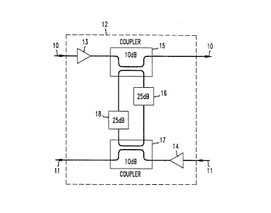
FIG. 1 shows an e~ ,1P- of an optical l~peat~,l 12 in accordance with
this invention. One or more of these l~ t~l~ 12 are located at l"~et~ P~
po~iti~n~ along the length of an optical tr~n~mi~sion system to amplify optical
signals pr~png~ting along the tr~n~mi~sion system.
The tr~n~mi~sion system cc",~,ises a first optical fiber 10 which carries
optical signals from a first terminal to a second termin~l, as in(1icnted by the arrows
in FIG. 1. The tr~n~mi~ion system also comrrises a second optical fiber 11 whichcarries optical signals from the second termin~l to the first termin~l As the optical
signals travel from one end termin~1 to another, they becc"~ pro~,ssively
20 n~ ~l Accordingly, one or more repe~ters 12 are spaced along the fibers 10 and
11 to amplify the ~ J~tc~3 optical signals. This ~mplifirnti -n is accon~plished by
an ~mplifiP~ 13 in fiber 10 and another ~mrlifiPr 14 in fiber 11. Any technique for
amplifying optical signals in an optical trnn~mission system may be used to
nrco..~l.lish the funclion of amplifiers 13 and 14. One eY~mrle of suitable
25 ~mrlificntion is a laær pul,l~d section of erbium doped optical fiber with power to
the laser S~-p~ by a dedic~tYl current line co~ P~t~l to the ~at~l. In sub~
~st~,~s, the first and æcond termin~l~ are located on shore and the fibers 10 and 11
and ,cipcat~.~ 12 are und~.-.at~.
Supervision or line ...on;to.ii g is ~rco...l lished via a perm~n~ntly
30 col~ne~;lt;d passive and lossy loopback circuit in the ,~i~ater 12. The loopback
circuit comrri~es an optical coupler located in the fiber 10 at the output line of
amplifier 13. The optical coupler 15 couples a portion of the signal in fiber 10 to the
input of an attenuatu, 16. The output of the ~ttenll~tor 16 is conl-ccl~l to the input of
an optical coupler 17 which is located in fiber 11 at the output of amplifier 14. The
2068926
-
- 6 -
optical coupler 17 couples a portion of the attçnuAt~d signal from A~l~ ..u~nr 16 to the
optical signal flowing in fiber 11 for return to the t~rmin~l tr~n~mitting alongfiber 10.
As described in more detail below, the optical signals in fibers 10 and 11
S contain a supervisory signal useful for idcn~irying and loc~ting faults in the optical
tr~nsmi~Sion system. The supervisory signal may be extracted from the rest of the
signal flowing into a l,..i-s~-;tl;.-g end station to give an in-lir~tir~n of any
deterior~tion in the trAn~mi~Sion system and the loc~ti~ n of any such deterioration.
The loopback circuit of FIG. 1 is bidirection~l In this regard, optical
10 coupler 17 also couples a portion of the optical signals flowing in fiber 11 to the
input of another ~lle~u5~ 18. The output of; I~ tor 18 is col~l-e.I~d to the input
of coupler 15, which couples a portion of the ~ '.4.~cf~ signal from a~t., ..~or 18 for
return to the termin~l tr~..~..~;ll;i~g along fiber 11. As in the case described above, a
supervisory signal is l~ t`h~l from the tefminAl ~ ;ng along fiber 11 and is15 looped back to that llAI-.~.ll;ll;l-g termin~l along fiber 10.
The loopback loss and mr~d~ tion index are chosen to minimi7~
degradation to the traffic signals on the ~lAI~ g and l~ce;ving lines and to
provide an adeqll~te level of loopback signals for in-service Illo~fi~ g For
eY~mrle, the in-service m dlll~tion index could be in the 1 to 10 percent range and
20 thetotalloopbacklosscouldbefromabout45dBfors~r,~msco~ -inguptoabout
300 l~,~at~.~ down to about 30 dB for S~ S having about 10 lepedt~
This is a simple and cost err~ al~ e to the pond.,l~,us
complexity of prior superv-isory ~ t.,..~ developed for electro optical l~gene.~t~.
The added .,~at~r cQ.--l~nf ~ in FIG. 1 include two coupl~ , which each may be,25 for eY~mrle, lOdB coupl~, and two optical ~ttenu~t~~rs~ which each may be, for
eY~mple 25dB Alh~ , providing a total of 45 dB of loss for each loQpback.
This simple but highly stable loopback path provides a means of ~ccllrAtely
the loop loss to any repeater from either temlin~l Studies have shown
that any change in system tr~n~mi~sion that is likely to affect service will be
30 identifi~ble as a change is .l~a~,d loopback losses. As the desc.i~lion belowmakes plain, the quantity that is actually llleasu~d via this technique is a relatively
low-L~uency amplitude mod~ tion of the average tr~n~mitted signal power. The
~mrlit~ld~ m~ tion remains coupled to the average signal power through the
~rocesses of amplifiration, dispe.~ion, and spectral bro~lenin~ due to fiber nonlins~r
35 effects. As ~ sse~ above, for in-service line ..~ni~. ;.-g, the amplitude
mo~ tion index is low, typically about 1 to 10 percent, preferably 2 to 5 percent, to
2068926
~inin~;,e signal degr~d~tir~nl For out-of-service .nonilu. ;ilg, the modlllAtion index is
increased to 100 percent replacing the high-bit rate data signals. Detection of the
supervisory portion of the loopback signal l~ui~s a technique which will now be
descnbed.
S FIG. 2 illustrates an e~ ,le of a circuit for t~n~mi~sion) l~co~ly, and
etection of supervisory signal l~lullled to the 11 ~n~ g telminAl via high loss
loopback circuits such as the one shown in FIG. 1. The circuit of FIG. 2 preferably
is located in one terminal of the optical trAn~mi~Si(~n system. FIG. 2 shows the two
optical fibers 10 and 11 of FIG. 1 and SChemAti~ y illusll~tes three l~at~ls 12a,
12b and 12c, one of which is shown in more detail in FIG. 1. The arrows in each
e~at(,r 12a, 12b and 12c s~lllboli~ the high loss loopback described above. The
number of l~a~rs used is dete-.-.in~d by the length of the trn~mi~sion system and
the l~uh~ed signal amplihlde along the fibers. Although not shown in FIG. 2, those
skilled in the art will appreciate that the fibers 10 and 11 are connect~l to similar
15 cil-;uil.~ in another t~rminAl They would also appreciate that the terminals would
be located on shore and the fibers 10 and 11 and the l~,~ate.~ 12a, 12b, 12c . . .
would be SUblll~ ed un~at~r in sub...A~;n~ appli~tion~. It is advant~geous for
only the sil~lesl and most reliable parts of a line .nr)~ or to be located in the
l~pc,a~rs and on the fibers. As the ~ sion here makes plain, this is achieved most
20 a~lmirahly in this in~ iol~.
A trnn~mit mnltirlçY~r in FIG. 2 produces a signal l~les~ .~;ng
info. ",AI;nn to be tlnn~ ;llc~d from the termin~l of FIG. 2 through the fiber 10 to the
other ~ A1 not shown in FIG. 2. The signal produced by the tran~mit
multiplexer 19 is one input to a mtxllllAt~r 20. The other input to the modlllAt~r 20 is
25 an optical carrier appeal~lg at the output of a laser ~ n;lh~ 21. The m~lll~tor 20
causes the optical carrier to be m~ te-l in accoldance with the i-~rol~--AI;on
col~ ed in the signal produced by the ~ smil multiplexer 19. The ~mplitllde of
the optical carrier is det~ ined by the output cur~ent of a laser bias circuit 22.
The alJpdlalus of FIG. 2 produces a supervisory signal useful in
30 idenlirying the presence and loc~ti- n of faults on the optical trAn~mi~ion system.
The supervisory signal col--p. ;~es a l~ c, pseudo random word produced by a
pseudor~ndom word gelle~dlol 23. Preferably, the bit rate and word length of thepseudo random words produced by the b_n~,~alol 23 are such that the word period is
longer than the round trip delay from the t~rmin~l to the l~ale~ furthest from the
35 ~An~ and back. For eYAmplc the word length may be 223 _ 1 bits at a bit rate
of 100 kb/sec. in a 10,000 km tr~n~mi~ n system. The input power level is chosen
- 20~8~26
-
- 8 -
such that the l~e~lUe; produçin~ signals and the supervisory signals do not unduly
inte.r~ with each other and the supervisory signal is con~eniel.lly l~,co~able at
the l~-.n~hing termin~l after loopback from the repeaters.
The pseudorandom words produced by the pse-ldorandom word
S ~n~,.alor 23 are one input to a modulatnr 24. A carrier signal, which may be a sine
wave or a square wave signal produced by a carrier source 25, is another input to the
mod~ tor 24. The output of the mnd~ tor 24 is the carrier from source 25 biphasem~lll~t,ed by the pseudor~qndom s~u~"lce from the pseudo random lu-~ber
gell~alol 23. The output of the mnd~ t~r 24 is connP~Ied to the bias circuit 22
10 which controls the bias current and, lLelef~l~, the amplitude of the optical carrier
signal from the laser ~ r 21. The supervisory signal thereby amplitude
modlll~tes the average power of the signal ~.,..-~...;l~ from the terminql alongfiber 10. ~lt~m~tively~ the supervisory signal could be linearly combil ed with the
output of the ~ ls~ mllltipl-~Y~r 19 and applied to modlll~r 20.
As eYrl~inPA above in conn.~!;on with a d~scli~)lion of FIG. 1, a portion
of this ~mrlitllde mo~ ted optical signal is looped back to the tr~n~mitting tf rmin~l
in each of the l~e~ . The loo~back signals from fiber 10, the signals from the
other temmin~l traveling along fiber 11, and any noise produced in the tr~n~mi~sion
system and traveling in fiber 11 is directed to a lecei~er 26 which coverts the optical
20 signals on fiber 11 to electlic~l signals. The l~ce;~,er 26 may, for ex~-ll~le, be a PIN
diode l~ice;~er or an av~l~nche pho~odet~ctor. The output of the receiver 26 is
connr~3 to a regene~dlor 27 which shapes and retimes the pulses in the signal from
the l~,ce;~,r 26. The shaped pulses are directed to a mllltipleY.~r 28 which receives
the info.... .......-l;on tl; ~-s~ d from the terrninal l.~ g on fiber 11.
As is ey~pl~in~ in detail with respect to FIG. 3, the l~igen~,ldtor 27 not
only pl~luces a data signal for reception by the multiplexer 28, it also produces the
inverse of such data signal. The unl~,~n~.lalc;d data signal from the l~,ce;~ 26 and
the inverse of the l~,ge~ t~,d data signal from the l~genc.alol 27 are input to a
c~nc~P,llP,r circuit 29 which is ill..~ l~l in more detail in FIG. 3.
The c~nc~llP,r circuit 29 adds the output of the l~ei~e. 26 and
subst~n i~lly the inverse of that signal so as to essent;~lly cancel the data signal from
the far te.ll~inal l~;...~n~ ;.-g on fiber 11, and thus reduce the inl~lre~nce caused by
that data signal with the .no~ o~;I-g function The output of the canceller 29 isco,-l-ect~l to the input of an ,R~ amplifier 30 which arnplifies the supervisory signals
35 thereby recovered from the signal on fiber 11.
2068926
.~. g
The amplified supervisory signal from amplifier 30 is then directed to a
series of deleclol~. There is a det~ct( l for each le~ater on lines 10 and 11. Each of
the det~ J.~ uses a correlation technique to pl~luce an output ~ se ~I;ng the
portion of the supervisory signal looped back by its lc;;lpec~i~e l~ater. That output
5 containsh~ro....~ nwhichcanbeusedtodete....illethe~,ro....Anceofthe
tr~n~mi~ion system out to the location of the l~ e l~atcr. Thus, the
existence and loc~tion of faults on the tr~nsmicsion system may be i-lentifi~d
One of the de~ ,.s 31 is shown in detail in FIG. 2. By way of
example, the d~t~clor 31 may be the clet~ o~ for l~ate. 12a. There are similar
10 det~ctorsforeachoftheotherl~ipe~e~ 12b, 12c . . . The~e~ector31 containsa
recdve pseudo random nUI11b~ ge-lP i ~or 32 which is s~nchl~l ized with the l.An~n~;t
pseudo-random number gr ~ tl)r 23, as in~iir~ted symbolically by line 33a. The
same clock which clocks the ~n~,.atol 23 also clocks the ~I~.a~ol 32. Cell~,.dlOl 32
pl.xluces the same pseudo random n ulllber sequence as ~ne.alor 23, but it produces
15 that sequence in a delayed fashion with respect to s~uence produced by
ge. e.alor 23. The m~pnit~lde of the delay is set to be equal to the round trip time
bel~.~n the tr-n~mit pseudo r~ndom num~. generator 23 and the l~ater 12a.
Each of the det~,cluls for the other l~,peate ~ contain delayed pl~ucl;on of pseudo
r~ldolll r.ulll~r sequences, the delay being equal to the round trip time bel-.~n the
20 producti. n of a pseudo random nulll~r by g_.le.alur 23 and the receipt of that
number after loopback by the l~pe~t.,. ~soci~te~ with that detector.
The pseudo random s~uelue pluduced by g_ne~alor 32 can be given a
ple~ete.-.~;ne~ delay with respect to the sequence produced by ~n~.alor 23 in any
~l~U~. For ey~mple~ the delay can be pr~luced by a counter preset by a
25 cO~u~ulcr 35 which sets the l~uilcd time delay in each of the dc t~lc~. ~ via an
interface such as an inh,. rar,e 34 and a delay control line 33a.
The number sequence from g.~ nrlntu~ 32 is directed to one input of an
exclusive OR gate 36. The output of the exclusive OR gahe 36 is connf~t~l to one of
the inputs of each of exclusive OR gates 37 and 38. The other input of exclusive OR
30 gate 38 is connec~d to the carrier source 25. The phase of the carrier from source 25
is shifted in phase by 90 in phase shifter 39. The output of the phase shifter 39 is
collllr~t d to the other input of exclusive OR gahe 37. The sequence from
~ne.dlol 32 thus bi-phase m~d~ tes two quadrature carriers via the exclusive OR
gates 37 and 38. The output of exclusive OR gate 37 is connr~ ;d to one input of a
35 multiplier 40. The other input of multiplier 40 is co~nrcl~ to the output of the RF
amplifier 30. The output of exclusive OR gate 38 is connected to one input of
- 2068926
- 10-
another multiplier 41. The other input of the multiplier 41 is col-nc~ d to the output
of the RF amplifier 30.
The multipliers 40 and 41 con~l;lu~e hol~olyne demod~ tors. The
output of each demod~ nr co~ n~ a DC col-lpol ellt pr~,lional to the product of
S the m~pnit~lde of the signal returned by l~Kat~,f 12a and the cos ~, where ~ is the
dirre.~.~ce in phase be~ the locally gene,ated carrier and that of the received
signal.
The output of mllltiplier 40 is con~ t~d to the input of an integrator 42
and the output of multiplier 41 is connecle~l to the input of another integrator 43.
10 The DC con~ponents produced at the outputs of multipliers 40 and 41 are integrated
by the integrators 42 and 43. In effect, the integrators 42 and 43 amplify the DC
COmpOI enl~ and ~U~pl~Ss the noise in the outputs of the multipliers 40 and 41. The
signal output caused by the DC col--~ol~nls in effect incl~,ase s with time, but the
noise does not affect the output of the inte~al~l~ bec~use it has a zero average value.
The outputs of the integrators 42 and 43 are in~lir~tion~ of the
~,. rV....~,.ce of the tr~n~m~ nn system from the ll..n~ ;ng termin~l to the
l~i~dt~,~ 12a ~soci~t~ with the det~,cte~ 31. Det~ction of the mq~ihlde of thoseouhputs and their ch~nges over time is a means by which the exi~tenre and locah-)n
faults can be identifi~.d in the lli.n~...;~siQn system. Similarly, the ma~nihlde and
20 ch~n~ s in c~ ;.~nding signals p~luced by the other de~clo~ s are an inflir~tion of
the existence and loc~tion of faults in the tr~n~mi~inn system in other loc~tiQn~
The ma~itude and ch~nges in ma~ni1llde in the det~ction signal may be
observed in any desired way to asct.ta~l tr~n~mics?on system ~IrOllll~l ce. In the
example of the invention shown in FIG. 2, the outputs of the inte~al~ 42 and 43
25 are sampled p~riodic~lly by sclc~lively connç~ g the inlfv~ tO~ outputs to analog to
digital con~it~ 47 and 48, via gates 44 and 45, which are closed by the OCCw~,l ce
of a strobe pulse produced on line 46 from the comp~t~r in~f,. r~ce 34. Con~e.t~,ls 47
and 48 pl~oduce digital n~.~ related to the m~nihlde of the voltages output by
the ir.t~,g.alc,.~ 42 and 43. The con~e.~ input those nul~ to the c(illlput~,r 35.
30 The numbers and their ch~nges over time may be observed to ..~I-;~or the
pe- rO. ..~ c of the tran~mi~sion system out to repeater 12a. For example, the
IIUI11~ may be squared and ~ccum~ t~l over a pred~ te ..-;~-ed measul~,ment period
to ~ccomrlish quadrature detection Quadrature del~lion is used becduse the phaseof the ~ceived carrier cannot, in general, be dete ..~inçd Let ~ = the phase
35 dirre~nce between the tr~n~mitted and received carrier. The outputs of the
multipliers 40 and 41 both are pl~ollional to the m~gnit~lde of the received signal,
2068926
A. They are also plu~l~ional to the cos(H) and the cos(~ + 2 )~ s~ vcly.
Squaring and adding the outputs yield A2 [(cos2 (~) + sin2 (0)] = A2, the
ma~itllde squared of the desired collll,o~
The integrator outputs are sampled when the strobe pulse on line 46 is
S high. The strobe line 46 is comlect~d to the clock input of a D flip flop 49, the output
of which is conl-~ d to one input of the exclusive OR gate 36 which also has theoutput of the receive pseudo random number ~n~lor 32 connp~-l~ to its other
input. On the falling edge of each strobe pulse, the D flip flop 49 is cloc~A causing
it to change state which, in turn, causes an inversion in the output of the exclusive
10 OR gate 36. Inversion of the ûutput of the exclusive OR gate 36 at each falling edge
of the strobe pulse causes a resulting inversion of the demr d~ q-tc-r carrier signals and
a change in the polarity of the d~ .n~ulqt~r output signals from the multipliers 40
and 41. The integrators thus ~IÇollll dual slope int~t.~ion, which çli...i~ ,s the
effect of any dc imhqlqn~e in the den~ r and in~ làt~1~7. The integrators may
15 be ac coupled by circuits whose time col.!~t~ are long co~ d to the sampling
period. The outputs of the in~çgr.qtors appl~ t~ triqn~ll-q-~ waves, which are
sampled at their turning points when the strobe line 46 is high. At the end of the
mea~,u~ lcnl~ the average lecei~cd signal at the integration output is given by
~ N ~ [Vln --Vln+1]2 + [V2n --V2n+l]2
20 where V 1 n and V2n are the nth sample values of the two integr~q~tir)n outputs and N
is the nulll~, of C~ plil-g intervals.
When the line ...oni~- l in accor~allce with this invention ope,~les on an
in-service basis, the l.,cc;~ed loopbac~ signals are ~,u~,. ;.--~s~l upon the data signal
~,~--~.--;l~ from the far tcfminq-l neC~ G the power ~7~;llUm of the data signal is
25 near n-~;n------ in the rlG~lucl c~l band of the line --Ol~;lJ~ signal, it is the dominant
source of in~rGlGnce. To reduce the int~,r~.c nce a data cqncell~r has been devised.
FIG. 3 shows a detailed eY~mrl~ of a canceller circuit which achieves a substantial
re~3ucti~n in inte,r~,lGI ce.
FIG. 3 shows the optical ~ecGhr~ r 26 described above and shown in
30 FIG. 2. The output of the optical lccei~r~ 26 is cQnn.o.cte~l to a reg~,n~ tor 50 which
shapes the data signal received from fiber 11. The output of the lGcei~er 26 is passed
2068926
through a delay ClC ~ .f,nt 51 and is directed to the input of a D-flip flop 52. A clock
signal for the D-flip flop 52 is lJ~uduced by passing the output of the receiver 26
through a high pass filter 53, a rectifier 54, and a band-pass filter 55. The Q output
of the flip flop 52 is a q~l~nti7~d version of the linear output of the optical lece;~r 26
S and is sent to the receive demultiplexer 28 of FIG. 2.
The Q output of the flip flop 52 is a qu~nfi7~A and inverted version of
the linear output of the optical l~,C~ .. 26 and is fed to the input of a variable gain
~mrlifier 56 whose gain is ~llu~ufic~lly controlled as described below. The output
of the receiver 26 is fed to the input of a delay element 57. The outputs of the delay
10 element 57 and the Amrlifi~r 56 arG filtered by identi~l band pass filters 58 and 59,
specli~/Gly. The output of band pass filter 58 is conne~t.,~l to one input of a
~u....~ g el~m-ont 60. The output of the band pass filter 59 is passed to another input
of the ~ .,,,,;ng elcmf,nt 60 via a switch Sl. The ~..n...~;ng element 60 produces an
output directed to the RF ~mrlifier 30 shown in FIGs. 2 and 3. That output is related
15 to the sum of the output of the lGce;l.e, 26 and the in~ ,d output of the
lG~nc.al~r 50. The data signal co.n~ f nt of the signal on fiber 11, and its possible
hlt~.r~ ce in the ~on;~ol ;.-g ~lC~Il, are thereby substAnti~lly elimin~t~d in the
output of the ~ il-g element 60.
A feeclb~c~ loop provides A~to.~AIi~ amplitude balance of the two
20 signals which are input to the s-J~- --~ing e4 ~f,-~ 60. In this regard, a rectifier 61
provides rec~ific~tion of p,~3ete ...;ny~ polarity, for e~ )le, positive polarity
rectific~ti- n, of the output of the band pass filter 58 and another rectifier 62 provides
oppo~i~ polarity recfific~tion, for example, ncgali~. polarity rectifir~tion, of the
output of the band pass filter 59. The outputs of the ~;~ifi~ 61 and 62 are summ~d
25 in a s-~.. ;l-g elem~nt 63, which produces an error signal at its output. The error
signal is directed through a low pass filter 64, the output of which is amplified by a
dc alllpliLif,r 65. The dc amplifier 65 produces an ~ulu...AI;c gain control signal
ct~d to d~e gain controlling input of the variable gain ~mrlifi~r 56. The feedb~loop provides ~ O...AI;f amplitude balance of the two signals before they are
30 ~.. ed and amplified in the RF amplifier 30. In ~ ition to gain control, ~ltom~fic
delay co~ nc~l;on may be used where the relative delay in the system is not
s-.ffi-~iently stable. The output of the RF amplifier 30 is conl-~led to the inputs of
correlation det~ctor~ such as the detectûr 31 shown in FIG. 2.
By ~ s~ing the data in~ Ç~, ellce by, say 20dB, the ll~asulG~nt
35 time can be reduced by a factor of about 100. This reduction in ll-easul.~ time
makes in service line moni~o~ ;ng feasible. Integration times, however, may be
2068926
- 13-
relatively long, for e~.nl le, several hours, which is why it is advantageous to use a
separate ~t~ O. channel for each çepeal~r in the system. This will permit
essenti~lly continlloue and collcu~ t .llo~ o.;.~g of the loopback losses of the entire
system. By idcntir~hlg loc~li7~ sources of degradation as they occur, ambiguides5 in loopback sign~hlres due a~ljacent degr~d~hon~ or rh~nges can be resolved.
In order to plan m~int~.n~nce, repairs, and l~;stulalions, it is highly
desirable to accurately measure system end-to-end margin and its v~ri~tion with
time. Margin is defined as the actual signal-to-noise ratio divided by the signal-to-
noise ratio n~xess~ y to meet error rate lc~lui~lll~l ls (eA~ ,ssed in dB). The
10 intc.rel~llce c~nr~ell~r described above in FIG. 3 can provide a lllea~ of the
received signal-to-noise ratio and hence the end-to-end margin. The c~nrell~tionratio of the c~ncellpr circuit is l"onolonir~lly in~ ai.illg filnction of the signal-to-
noise ratio. That this should be true can be undc.~od by the following rea~oning.
The c~nr~llçr forms the dirL.~nce of two signals, one of which ~,l,v~n~ the true15 signal that has been disl~Jrt~d (multiplied by a consl;~nt) plus additive noise. The
other is the true signal that has been l~g_n~l~t~. The first order effects of distortion
can be co.~ e nc~ by linear weighting The reslllting dirr~ ce between the two
signals, when divided by the value of the ~cei~,cd signal plus noise equals
N + S
20 which when inverted and e A~ ,ssed in dB equals the c~nr~ellçr ratio. The canceller
ratio is analogous to the noise power ratio co.. nl-ly used to evaluate signal-to-
noise ratios in Ll~uency division multiplexed analog tr~n~mi~sion s~ms. The
c~nrellçr ratio very closely appç~ Çs the ratio of signal density to noise density
I-~c~su l through id~ntir~l bandr~s filters. It follows that by pçri~1ir~11y
25 Illon;~- ;n g the c~nr,ell~tion ratio sh~ng~s in margin can be detecte~1
In the circuit of FIG. 3, the c~nc~ tion ratio may be det~....inf d by
directing the output of RF ~mplifiçr 30 to a rectifier 66, then through a low pass
filter 67, and finally to a voltage ll~ uling device 68 such as a voltmeter or
com~ r. The cancellation ratio equals the reading taken by the voltage measuring30 device 68 where switch Sl is open divided by the reading with switch S 1 closed.
The result is an in~ic~tion of the overall signal-to-noise ratio or end-to-end margin of
the tr~n~mi~sion system.