Note: Descriptions are shown in the official language in which they were submitted.
` 92 0~ `~) 2~ 27 ~3 3208 1~;44 ARI~IIKA&IZUMI 1~ 3
2069243
Logarithmic Intermediate-Frequency A~pl~fier
BACKGRO~ND OF THE INVENTION
1~ Field of the Inventio~
This invention relates to a logarithmic intermediate-
frequencY amplifier, and more psrticularly, to a logarithmic
intermediate-frequency amplifier having true logarithmic
characteristic or pseudo logarithmic characteristic.
2. Description of the ~elated Art
In general, a logarithmic intermediate-~re~uency tIF)
amplifier comprises IF amplifiers cascade-con~ected to sach
other in a multistage connectiou ma~ner, rectifiers for
receivin~ output signals o~ these IF amplifiers in a
successive ma~ner. and an adder fox adding all output
sig~als o~ these rectifiers to each other, and is generally
formed o~ a bipola~ inte~r~ted circuit. ~his is based on
such advantageous facts that bipolar transistor is superior
in noise charact~ristic as well as small in sensltlvity
degradation when considered ~rom the viewpoint o~ a recei~ed
input. and it can be driven even at a low imped~nce or at a
large capacity because the bpolar tr~nsistor has a high
drivability and the like.
' g2 ()5 ~ 20 27 ~03 S2118 ~)~34~ ARIHIKA&IZUMI ~ 4
20692~3
Rece~tly, a C-~OS logarithmic IF amplifier has been
demanded to be developed in order to effectivelY use the
advantages of the C-~S inte~rated circuit. In this case,
however. the following problems have been ponted out on
a structural basis:
An MOS transistor is large In l/f nolse, so that it is
required ~o have an i~termediate-frequency (~F) band cut off
its low band side i~ order to pre~e~t tho sensit hity from
bein~ degraded from the viewpolnt of a received input. So-
called HPF (High Pass Filter) characteristic to cut off this
low band ~ide can be equivalently obtained by ~roviding ~F
amplifiers ~n a multista~e casczde-con~ection manner through
coupling capacitors. In this case, bowever. a coupling
capacitor to be inserted is desired to be small in capacit~.
O~ the other hand, the multistage connection of the IF
amplifiers throug~ the coupling capacitors makes that the
rectifiers receiving output s~gnals of respective IF
amplifiers differentiate the slgnal waveforms thereof, thus
making it easy to vary the drect-current value of an output
of each rectifier. As a result, in order to obtain a good
li~ear logarithmic chara~teristic, it is unavoidably
required to e~pand the frequency band of an input signal of
~ 2 --
' ~2 OF ~ 2~ 28 ~03 3208 06~14 ARI~HII~A&IZUMI (2~t~J5
20692~3
each rectifier to the low requency side. that is, it is
requ~red that the capacity of a coupliu~ capacitor to ~e
insertedly used is increased.
Accordingly in order to practlcally r~allze tbe C-~OS
logarithmic ~F amplifier, such a proble~ has been arisen
that for the capacity of a coupling capacitor to be used,
su~h contradicto~y requirements as shown above must be
satisfied. ln addition. in case that the capacity of a
coupling capaci~or to be used is inc~eased, thare arises a
problem on the dri~ability of the IF amplifier itself as
well.
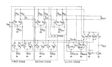
Negt, as a pseudo - logarithmic I~ ampli~ier of
polygonal llne ~pprogimation type formed on a C-~OS
integrated circuit, such a circuit as is, fo~ e~amPle, shown
in Fig. 1 is ~nown conventionally. This ~ircuit ls disclosed
l~ the Japanese Laid-Open Patent hpplication ~o. 62-292010,
which comp~ises n differential ampl~fiers respectively
~ncluding ~OS tra~sistor pairs (T~l, TOl), (T02. T02), ....
and ~TOn, TOn) and constant-current sources IOl, IO~, ....
a~d IOn. These different~al amplifiers a~e cascaded in a n-
stags connection manner. The differential a~plifiers of the
first through nth stages ~re connected to full-wave
' 92 ()F `~ 2(1`2~ ~)3 32(~8 ()ff44 ARIHIKA&IZUMI C~ )6
2069243
reGtifiers comprising two pa~rs o~ transistors (Tll and
Tlk), ~T21 and T2k), .... and ~Tnl a~d Tnk). and n co~stant-
current sou~ces Ill, I12, .... and Il~ for driving these two
pairs of tr~nsistors, respectively. The dIfferential
amplfier of the (n+l)th stage has a full-wave rectifier
co~prising two pairs of ~05 transstors ( T(ntl~, and
T(n~l)k) and two constant-Gurrent sources In(n+l) for
drving the two pairs of them, and receiving an output
signal of the differential amplifier at the nth ~tage.
These ~ntl) pairs of transistors (Tll and Tlk). (T21
and T2k), ..., and (T(ntl)l and T(n~l)k) forming full-wave
rectifiers each has a ga~e-width (W) and gate-lengtb (~)
rat~o (W~L) of l:k (~>1) tbereby to constitute an unbalan~ed
differential pair. The~, in respectlve two pairs, the
t~ansistors havi~g a gate-width (~ and gate-len~th (13
ratio (~/L) of one (1), or (T11 and Tll), (T~l and T21),
, and ~T(ntl)l and T(ntl)l) have the drai~s and ~ates
connected respectively in co~on, and on the other hand,
those having the ratio (W~L) of k, or the tra~sisto~s ~Tlk
a~d Tlk), (T2k and T2k), -, and (T(ntl)k and T(ntl)k) ha~e
the drains and gates co~nected respec~ively in co~on.
Ne~t to the (n~l)th stage, ~n adder co~p~ising t~ee
` ~32 (~ ` 2(~ 3(:~ ~n3 3208 l~G~14 ARICI~IKA&IZUMI ~1007
2069243
~OS transistor pairs (T10, T2~), (T30, T4~) and ~T50, T~0)
ls provided, which sums up the outputs of the full-wave
re~tifiers of the first to the (n~l~th sta~es.
~ ith the pseudo-l~garithmie IF amplifier arranged as
above, the operation will be described below.
Flrst, a tr~nsconductan~e parameter ~ can be expressed
in terms of the gate-width and gat~-length ratio (~ll/Lll)
of the transistor Tll on the first ~ta~e by the followin~
squation (1);
~ (Co~/2) (~
where, ~ n is a mobility of ~OS transistor; and ~ox is a
gate o ide film capacity pe~ unit area.
In addition, ~ith the transistor pair (Tll, Tlk) o~ the
first stage, a ratio k between the gate-widt~ and gate-
le~gth ratio of one translstor Tll of the pair and that of
the ~ther transistor Tlk ca~ be expressed as foll~ws;
(Wlk/ Llk)
k= ~ (2)
(Wll/ Lll)
-- 5--
' 92 ~)E ! 2~1 30 ~3 3~ 01349 ARI('HIKA&IZUMI Ql~
20~92~3
~ urther in addition. ln the two pairs of transistors
tTll and Tlk) of the first stage, if the gate-to-source
voltag~s of respective t~ansistors are e~pressed as Vgsl,
Vgs2, Vgs3 and V~s4, and the threshold voltage of eac~
tra~sistor ls expressed as Vt. the cur~ents of respeetive
t~ansistors Il, I2. I3 and I4 can be e~pressed as follows;
Il - a (Vgsl - Vt)~ -~- (3)
I2 = ka (Vgs2 - Vt)2 ~ (4)
13 = a (Vgs3 - Vt) 2
I4 = k~ ~Vgs4 - Vt~ ^- (6)
~ ere, t~ese currents Il, I2, I3 aQd I4 can be e~pressed
in terms of a current Ill of the oonstant-curre~t source of
the first stage as follows;
II t I2 - Ill - ~7)
13 t I4 = 111 (8)
` 92 ()F ` 2~ ~31 ~03 3208 (~644 ARICHIKA&12UMI l~lrJ~)9
20~9243
Also. an input voltage VIN of the two p~irs of-
transistors (Tll and Tlk~ of the fi~st stage ca~ be
e~pressed in terms of the gate-to-sourc& voltages Vgsl,
Vgs2, Vgs~ and Vgs4 o~ the transistors as follo~s;
VIN - Vgsl - Vgs2 = Vgs4 - VS3 (9)
As a res~lt, an output current ~ Il of the two pairs of
transistors (Tll a~d Tlk) can be expressed as follows;
Il = (Il - I2) - ~I4 - I3
-Z(l - l/k) ~(1 t l/k) Ill - 2~ VIN~
~ ~ (10)
(1 t 1/ ~
From ~q.(10), it c~ be ound that the output current
~ 11 ha~ a square ~ull-wave rectifica~lon characteristic
with respect to the input volta~e VIN.
In the same manner as above, an output current ~ I2
of t~e t~o pairs of transisto~s (T21 and T2k) of the
second stage - , and an output current ~n~l of the two
~2 05 2~) 32 ~e~3 3~()8 ~644 ARI~HIKA&IZlJMI Q1~10
20692~3
pairs of the transistors (T(n+1)1 and ?~n+l)k) can be
respectively e~pressed as follows;
-2(1 - l/k) {(1 t 1/k)-I22 - 2a VlNP3
(1 + 1/ k)2
-2(1 - l/k) {~1 + I/~) I(ntl) 2a VOUT
a In+l ~
(1 t 1~ k) a
(12)
Here, t is clear that the output currents ~ Il,
I2 -, ~ In+1 and the constant-curre~t sources I11. I22,
~, and I~(n~l) of respective stages are related as shown
by the following equations (13) to (15);
-2I11 S ~ 2I11 (13)
-2~22 ~ ~ I2 ~ 2I22 ~(14)
' ~2 V5 2~1 32 ~13 32~8 l644 ARIC~lIKA&IZllMI 1~
- 20~9243
-21n(n+1) ~ ~ In~l ~ 21n(n+1) o (15)
Thts mea~s that even if the i~put voltage VIN and the
output vo1tages Vl, V2 ^ , Y~UT of respective stages a~e
made large, the output currents ~ Il. ~ I~---, ~ In~l are
always ~ithin the respective ran~es shown bY Eqs.(l3) to
(15). In addition, the volta~e ~l. Y2, ..., V~UT are output
voltages of the d~fferential ampli~iers of respecti~e
stages. and as the input voltage VIN is increased gradually,
these voltage~ are su~cessively saturated in the order of
VOUT, - V2, and Vl.
Also, ~he output current IOUT of tbe adder consisting
of the three UOS transistor pairs (T10, T20), (T30, T40~ and
(TSû, T6~) c,in be expressed as follows;
IOUT = A I l ~ ~ I2 t . . . ~ ~ In+l ~ (16)
As a result, by suitably setti~g the constant current
values I01, I0~, ~- , and I0~ of the constant-current
sources of respective stages and the resistance values ~0l,
` ~2 OE . 20 33 '~33 32~ 6~4 ARICIIIKA~ IZUMI 1~1~)12
2069243
R02. , ~nd ~On of resistors to be connected to the drains
of respective transistors, the maximum output voltages of
the differental amplifiers of respective stages can be made
of a constant sign~ T~is 3eans that the charaeteristic o~
the output current IOUT can be made appro~i~ately of a
logarithmic characte~istic to the input voltage VIN.
~ ith the conventional pseudo-logarithmic I~ amplifier
arranged as shown above, it makes one full-wave rectifier
of two unbalan¢ed differential tra~sisto~ pairs and as a
result, the constant-current source is required to be used
twlce in nu~ber as many as the rectifier, resulting i~
arlsln~ suc~ a problem that current eonsumptlon unavoidably
becomes lar~e. In addition, considerin~ from the viewpoint
of the circuit structure. one rectifier uses two u~balanced
differential transistor pairs and as a ~esult. the circuit
scale disadva~tageously becomes large.
This lnventio~ was made wlth a view to solvi~g the
above-mentioned problems. an obJect of this invention is to
provide a logarithmic IF amplifier i~ which contradictory
requirements on the capacitY of a coupling capacitor to be
inserted can be satisfied thereby to be formed on a ~-~05
integrated circuit~
-- 10--
' 92 ~ 2~ 34 ~3 32~18 ~644 ARICHIKA&IZUMI [~11313
2069243
Another object of this inventlon is to provide a
pseudo-logarithmic IF amplifier capable of reducing power
co~sumption as ~ell a~ decrsasing circuit scale.
As the applications related to this invention. the
followi~gs are concerned; the ~apanese Patent Application
No. 2-292866 previously made by the same a~pl~cant; the
U. S. Patent Application No. 784.5~2 which was made
correspondingly thereto; and the British, German and French
Patent Application No. 91310038.4 based sn the European
Patent Co~vention.
SUMUAR~ OF T~E ~NVENTION
~I) In a first aspect of this invention, a C-~OS
logarith~ic IF amplifier is provided which is realizable
on a C-~OS integrated circuit.
~ C-~OS logarithmic I~ amplifier of this aspect
comprises a plurality of lF amplifiers cascade-con~ected
through a first coupling capacitor to each other, a
plural~ty of rectifiers each receivlng a signal from the
correspondlng one of the IF amplifiers through a second
coupling capacitor dif~erent in capacity from the ~irs~
coupling capacitor, and an adder for adding the output
)r ~ 20 ~4 ~n3 32(~8 0644 ARICHIKA&IZUMI b~l~l4
2069243
signals of the rectifie~s to each other.
~ ith the C-NOS logarithmic IF a~plifier arranged as
above, the first and sec~d coupling capacitors are
preferable to be connected in series to each other thereby
cascade - Gonnecting the IF amplifiers therethrough. The
rectifiers each is applied with a~ output sig~al of the
corresponding one of the I~ a~plifiers at the connection
point of the corres~ondi~g first and second coupli~g
capacitors.
An IF amplifier to be used for this i~ventlon is not
specificall~ limited in structure thereby. an arbitrarily
structured one can ~e ~ed therefor, and a rectifier to be
used ~or this invention is not specifically limite~ in
structur~ thereby, so t~at either o~ a half-waYe or full-
wave rectifier ca~ be used therefor.
Wi~h the C-~OS logarithmic IF amplifier of this aspect,
the IF amplifiers are connected through the first coupling
capacitor to e~ch other and the rectifiers are connected to
each other through t~e second coupling capacitor different
in capacity from the first coupling capacitor. As a result.
by setting t~e first and second couplng capacitors at
optimum capacitive values ~espectively, the IF amplifi~rs
"32 ~F ' 20 35 ~)3 3208 ~44 ARIHIKA&IZUMI 1~lol5
2069243
each makes it possible t~ have its frequency band cut off
the low band side thereof, and the rectifiers each makes it
possible to ha~e its frequencY band e~panded to the low band
side. Accordingly, (l/f) noise of an IF amplifier can bs
reduced the~e~y restricting deg~adation o~ noise figure
(NF). In addition, the Input band of a rectifier can be
expanded to the low band side thereby obviating e~cessive
signal differe~tiation and positiYely maintaining linearity
of the logarithmic characteristlc. Consequently, the ~-~0$
logarithmic IF amplifie~ accordin~ to this inv6ntion ca~
be reali2ed on a C-~OS i~tegrated circuit.
(2) rn a second aspect of thi~ inve~tion. a pseudo-
loga~ith~ic IF amplifier is provided which is realizable on
a ~-~OS integrated circuit. This amplifier has two types, a
first and second~
A pseudo-l~garithmic IF amplifier of the first type
comprlses a plurality of differential amplifiers cascade-
connected in a plurality of stages, a f~rst ~alf-wave
rectifier for receiving an input signal of the dif~erential
amplifier of a ~irst one of the stages, a plurality of
second half-~ave rectifiers each receiving a~ out~ut signal
of the cor~e~ponding one of the differential a~plifiers
- 13 -
~ 2~ 36 ~3 32~18 Q644 ARICHIKA~IZUMI (~ 16
2069243
other than that at the first stage, and an adder for adding
the direct-current components of outputs of the first and
second recti~iers. The first and second rectifiers e~ch has
one or mo~e unbalan~ed differential transistor pairs
different in ~ate-width a~d gate-length ratio from each
other thereby outputting the dlrect-current component o~
a differential output current of the same.
A pseudo-logarithmic IF amplifier o~ the second type
comprises a plurality of differential amplifiers cascade-
connected in a pluralitY of stages, a first half-wave
rectifi~r fox receiving an i~put signal of the dlfferential
amplif~er of a first one of the stages. a plurality of
second half-w~ve rectifiers eaGh receiving an output signal
of the correspondin~ one of the differential amplifiers
other than that at the first stage, and an adder for adding
outputs of the first and second half-wave rectifiers and
outputtin~ the direct-current components thus added, or for
receiving outputs of the ~irst and second rectifiers to fon~
their direGt-current compo~ents thereby to be added to each
other. Similar to t~e first type, the first and second
rectifiers each has one or more unbalaneed differential
transistor-pairs different in gate-width and ~ate-length
' ~2 ~5 `' 20 37 ~)3 32~8 ~)~3'14 ARICHIKA&IZUMI ~1~317
2069243
ratio from each other, but different from the first type in
that ea~h of them is so structured that is adapted to output
its differential outPut current dlrectly.
~ ith the first and second types of the pseudo-
lo~arith~ic IF a~plifier in this aspect, in cas~ that two or
more unbalanced differential transistor-pairs di~ferent i~
gate-~idth and gate-length ratio are to be provided, it is
pre~erable that the translstors each with a relatively small
gate-width and ~ate-length ratio have the drains and gates
connected resp~ctively in commo~, and the transistors each
with a relatively large ~ate-width and gate-length ratio
have the drains and gates connected respectively in ~ommon.
With the pseudo-logarlth~ic IF amplifier according to
this invention, a half-wave rectifier having one o~ more
unbalanced differential transistor-pairs is used as the
rectifier, and a direct - current component of its
dlfferential output current is added, or its differential
output current is added and then, ~he direct-current
component is taken out therefro~. As a result, current
consu~ption a~d circuit scale ca~ be advantageouslY reduced.
In addition, when two or more unbal~nced differential
tranSiStQr pairs are provided. an improvement in llnear
- 15 ~
' 92 ~F ` 2~`37 ~03 3208 ~)~44 ARICHIKA~IZUMI ~ )18
20692~
of logarithmic characterlstic results as compared wlth the
case that one pair of them is used.
~RIEF DESCBIPTION OF T~E D~A~INGS
Fig. 1 is a circuit diagram showing an e~a~ple of a
conventional pseudo-logarithmic I~ amplifie~.
Fig. 2 is a circuit block diagram of a C-~OS
logarithmic IF amplifler acco~di~g to a ~irst embodimeut of
this inve~tion.
Fig. 3 is a circuit block diagram of a C-~OS
logarithmic IF ampli~ier accordi~g to a second embodiment of
this invention.
Fig. 4 is a circult diag~am showing o~e e~ample o~ a
rectifier to be used in the amplifier show~ i~ Fig. 2 or 3.
Fig 5 is a circuit diagram showing another e~ample o~
a rectifier to be used in the amplifier shown in Fig. 2 or
3.
~ ig. 6 is a circuit d~agrRm of a pseudo-logarithm~c I~
amplifier accordi~g to a third embodlment of this inven~ion.
Fig. 7 is a characteristlc diagram o~ the amplifler
shown i~ Fig. 6.
Fig. 8 is a circuit diagram of a pseudo-logarithmic IF
- 16 -
' 92 ~5 ` 2~ 38 ~3 32l~ 0~;44 ARICHIKA&IZUMI 1~ 9
20~92~3
amplifier according to a fourth embodiment of this
invention.
Fig. 9 is a circ~it diagram of a pseudo-logarithmic IF
a~plifier according to a fi~t~ e~bodime~t of this inve~tion.
Fi~. 10 is a circuit diagram of a half-~ave rectifier
to be used in the amplifier shown in Fig. 9.
DESC~IPTION O~ T~E PREFE~ED EMBODI~ENTS
The preferred embodimen~s of this inYention will be
described below whil~ referring to Figs. Z to 10.
CFirst E~bodime~t]
Fig. 2 shows a C-NOS lo~arithmic IF amplifier according
to a ~irst embodiment of this i~vention, in ~ich a
plurality of IF a~plifiers ~1, A2, are cascaded ln a
multistage conne~tio~ manner in order to amplify an IF
signal successively. The multistage cascade - connected
a~plifiers Al, A2,--- have rectifiers Bl, B2,--- connected
t~ereto in order to recti~Y their output signals,
respectively. ~utput signals of the rectifi~rs Bl, B2.
are sent to an adder C to be added to each other and
outputted. The I~ ampli~iers ~1, A2, ~ the rectifiers Bl,
`~2 ~5 2~ 3g ~l)3 3208 ~1~44 ARlCHlKA&lZllMI ~c~2~
2069243
B~. and th~ adder C are respectively made of ~OS
t~ansistors.
These IF amplifiers Al, A2, -- are cascade-connected
to each other through the two capacitors which are connected
in series between each adjace~t two of these IF amplifiers.
Each of the IF amplifiers A1. ~2,~ s connected to the
correspondin~ one of these rectifiers B1, B2, - at the
connection point of the two capacltors connected in se~ies
therebetween. Namely, the IF amplifiers Al and A~ are
cascade-connected to each other throug~ the capacitors ~A1
and CBl which are disposed in se~ies therebet~een. The IF
a~plifler A1 is ~o~ected to ~he rectifier B1 at the
connection poi~t of the capacitors ~Al and CBl. In addition,
the IF amplifiers A2 and A3 are cascade-connected to each
other through the capacitor~ CA2 ~nd CB~ which are disposed
i~ series therebetween, and the IF amplifier A2 is connected
to the rectifier B~ at the connectio~ point o~ the
capac~tors CA2 and CB2. The IF amplifie~s A3 and A4, ~4 and
A5. are cascade-connected to each other ~nd connected
correspondingly to the rectifiers B3, B4, in the same
manner as shown above.
In the fo110win~ description. an IF amplifier Ai,
- 18 -
' 92 ~)5 ` 20 4~ ~3 32~3.'3 OG44 ARlCHlKA&lZllMI ~lt~2l
2069243
recti~ier Bi and capacitor CAi a~d C~i (i = 1, 2, )
typically sh~w there amplifiers. rectifiers and capacitors,
respectively. Thus. an input signal to a rectifier Bi is
supplied t~ the gate of a MOS transisto~ thereof, so that
the input impedance becomes high and yet the direct-current
biasi~g to th~ gate can be made of a higb lnput ~mpedance.
As a result, if the input i~pedance o~ the rectifier Bi is
neglected, a combined capacity Ci of the capacitors CAi and
GBi can be appro~imated as ~ollo~s,
Ci . (CAi CBi)~(CAit~Bl) (21)
That is, the IF amplifiers Ai and A(i~l) are coupled
through the combined capacity Ci to each ot~er~ and the IF
amplifier Ai and the recti~ier Bi are coupled to each other
through only the capacity o the capacitor CAi.
In additionj the low band side of a frequency band is
deter~ined by the differential characteristic ( ~PF
characteristic) of each coupling capacitor. As a result, the
ratio of a low band side ~ut-off ~requencY fcIFi of t~e IF
amplifier Ai and a lo~ ba~d side cut-off frequency fc~ECTi
of the rectifier Bi ca~ be e~pressed as foltows
- 19 -
' ~2 0~ ` 2~ `4~ )3 32~8 O~i44 ARl('HlKA&lZllMI ~1~)22
206~243
fcIFi/fcRECTi ~ CAi/Ci - (C~i/CBi) t 1 (>1) (22)
~ ro~ Eq.(~2). it can be found that the low band side
cut-off frequency fcIFi of the ~F amplifier Ai can be made
high compared with the low band side cut-off frequency
~cRECTi of the rectifier Bl~
In this case, a load capacity of the TF ampli~ier Ai is
the combined capacity Ci, howeve~, if C~l = CBi = Co. from
Eq.~21), Ci - (1/2) Co, which means that the capacity of an
inter-sta~e coupling capacitor of the IF amplfier Ai
becomes half that of a coupling c~pacitor with the rectifier
Bi. As ~ result. from Eq.(22), fcIFI = 2fcRECTi is obtained,
whlch means that the low band s~de cut-off frequency of the
rectifier Bi can be decreased up to a half of that of the IF
amplifier Ai.
Conseque~tly, according to this invention. an IF
~mplifier ls allowed the low band side of its frequency band
to be cut off and on the other hand, a ~ectifier is allowed
lts frequency band to be e~panded to thc low band side, so
that a logarith~i~ IF amplifie~ can be obtain~d ~hich is
~ormed o~ a C~~OS inte~ated circuit without arising any
- 20 -
' 92 ~ ` 2~ 41 ~l)3 3208 ~644 ARICHIKA&IZUMI b~l023
2069243
important problem.
[Second Embodiment]
Fig. 3 shows a C-~OS logarithmic IF amplif~er according
to a second embodîment of this invention. In Fig. 3, an IF
amplifier Ai is connected through a capacito~ CBi to an IF
amplifier ~(i+l) and through a capacitor CBi whose capacity
is different from that of the capacitor CAi to a rectifier
Bi. Other co~ponents are arranged as e~plained in the first
embodîment. The C-~OS logarithmic IF amplifier of this
embodiment makes it possible to obtain the same effects as
shown in the first embodiment.
[First Exa~ple of ~ectlfier to be used in First and Second
Embodimants]
In the fir~t and second embodiments, any ci~cuit made
of ~-~OS transistor can be arbitrarily used as the rectifier
Bi. In this case, however. a squarlng circuit can be pointed
out as an e~ample as shown i~ Fig. 4, which is disclosed n
the Japanese Laid-Open Patent Application No. 63-24377 made
by the same one as the i~vento~ o~ this amplifier, thus
being used as a squaring full-wave rectifier.
- 21 -
' 92 ~)E ` 2~ ~2 ~03 32t~8 0644 ARICHIKA&IZUMI 121~)24
20692~3
In Fig. 4t the squaring clrcuit co~prises a first
dlfferential tra~slstor-pai~ co~sisting ~f a ~OS transistor
Tl with a gate-width and gate-length ratio (Wl/Ll) and a ~S
transistor T2 with a gate-width and gate-length ratio
(~2/L2) and a second differential transistor-pair consisting
of a MOS transistor T3 with the same ratio as that of the
tra~sistor Tl, (Wl/LI), and a ~S translstor T4 with the
same ratio as that of the transisto~ T2. (W~12). In this
case, if the ratio (~ 13 is made one (l), the ratio
(WZ/L~) is made k. The transistors Tl and T2 have the
sources connected in common and the transistors T3 and T4
have the sources connected in common, which are connected
through their co~nect~on points to constant-~urrent sou~ces
IO, respectively. The gate of the transistor Tl is connected
to that of the transistor 4, and the gate o~ the transistor
T2 is connected to that of the transistor T3. The collector
of the transistor Tl is co~ected to that of the transistor
T3, and the collector o~ the transistor 2 is counected to
that of the c~llecto~ T4. An input voltage ~I~ is applied
ac~oss the common gate o~ the tra~sistors Tl and T4 and the
co~on gate of the transistors T~ and T3, which are
dî~fere~t i~ the gate-width and gate-length ratio from each
- 22 -
' 92 ~F ' 2~3`4~ t~03 320~ 44 ARICHIKA~IZUMI 1~025
2069243
other. Transistors T5 and T6 each îs the primary side
transistor of a current mirror circuit. A subtracting
circuit S subtraGts a current flowing in the output line of
the second differential pair from a current flowing in the
output line of the flrst differential pair. VDD is a voltage
source.
With the circuit arranged as above, the characteristics
will be e~plained below.
Drain curre~ts Idl and Id2 of the transistors Tl and T2
of the first differential p~ir and drain current~ Id3 and
Id4 of the t~ansistors T3 a~d T4 of the seco~d di~fere~tial
pair can be e~pressed as follows;
Idl = a l(VGSl - VT)~ -- (23)
Id2 ~ k(VGS~ - VT)2 (24)
Id3 - a l~VGS3 - VT)~ ---~ (25)
Id~ ~ a l kl(VGS4 - YT) 2 , (2g~
where. VGSl, VGS2, VGS3 and YGS4 ar~ gate-to-source voltages
- 23
.
i
~ g2 ~5 . 2~ 43 ~3 3~1)8 t644 ARICHIKA&IZUMI ~026
20~9~93
o~ the translstors T1, T2. T3 and T4, respectively. a~d VT
is the thresho~d voltage of each transistor.
In these equations, if the ~obility of an electro~ of
NOS transistor is e~pressed as ~ n and the gate o~ide fi1m
capacity per unit a~ea of MOS t~ansistor is expressed as
CQ~, the followin equatlons can be obtained, as
a 1 ~ ~ n(CO~/2) (W1/Ll) (27~
kl - (W2/L2~/~W1/Ll~ ...--(2B)
In addition; the eonstant-current value I0 of the
consta~t-current source, and t~e i~put voltage VIN can be
e~p~essad as follows;
Idl + Id2 = I0 ......... (~g)
Id3 t .Id4 - I0 ........ (30)
VGSl - VGS2 = ~IN ---- (31)
V&S3 - VGS4 - VIN (32)
- 24
~ 92 ~6 2~ 44 ~03 3208 ~1~44 ARICHIKA&IZUM~ 27
20692~3
~lere, if Q IdI Ls de~ined as
~ Idl ~ Idl - IdZ ~33).
it can be obtained by the following equation. as
IdI = C-tl+l/kl) (l-l/kl)IO t 2a 1 (l~l/Kl) VIN2 ~
4~ l VIN ~ 8) {(l+l/~l)(IV/~ INZ)}'~]/(ltl/kl)2
..... ~34).
In addition, i~ ~ ~dII is de~ined as
~ I~l I = Id3 - I~4 - - - (35) .
it can be obtained as follows:
IdII Y [(ltl/kl) (l-l/kl)IO t 2a l (l-l/Kl)VIN~ +
4a l VI~ 2~{(1tl/El)~IO/~ l)-YIN2)~Z]/(l+l/kl)2
(3~)
Hence I
Id - ~ IdI - ~ IdII
-- 25--
` 92 ~ 2(1 44 ~3 32l~8 ~31i44 ARICHIKA&IZUMI ~ 28
20692~3
= [-2~1+1/kl) (l-l/kl~10 + 4a l~(l-l/El)VIN2]/(ltl/kl) 2
~ -(37)
From Eq.(37), lt can be fo~nd that the current difference
Id includes ths squar~ term of the input voltage VIN.
In the other hand, the current dfference ~ Id ~an be
e~pressed as follows;
~ Id = (Idl ~ Id3) - (Id2 ~ Id4) - ~ 38)
From Eq.(38), it can be found that such an output current
that is e~pressed by Eq~(37) including the square term of
the in~ut voltage VIN can be obtainad by the subtr~ctin~
clrcu~t S.
As e~plained above, the square characteristic can be
obtained with a simple circuit arranged as shown i~ Fig. 4,
which comprises two dif~erential pairs each consistlng of
two transisto~s dif~erent in the gate-width and gate-lenth
ratlo (W/L) from each other, and iE which the trsnsistors
with the same gate-width and gate-lengt~ ratlo (~/L) have
the drains connected in common to each other a~d yet, their
outputs beco~e opposite in phase.
- 2~
' 92 or ~ ~n 45 ~P03 3208 0~4 ARI~HIl:A&IZl)MI l~ g
2069243
[Second E~ample o~ RectIfier to be used in ~lrst and S~cond
Embodiments]
Another e~ample of a squarin~ circuit to be used Ln
these embodiments is s~ow~ in Fig. 5. which comprises four
MOS transistors. In Fig. 5, ~OS transistors ~1 and M~
constitute a first di~ferentia1 transistor-palr to be driven
~y a constant-current source IO, and ~OS transistors M3 ~nd
N~ constitute a second differential transistor-pair to be
driven by ~ constant-curre~t source obtained by the
following equation;
{2-k2l'2/~k2tl~}.Io .,...~39)
Further in Fig. 5. the dr~in of the transistor ~1 is
connected to that of the transistor M3, a~d the drain of the
transistor U2 is connected to that of the transistor ~4. The
gate of t~e transistor Ml is connected to that of the
transistor ~4, and the gate o~ t~ transistor ~2 is
connected to that of the translstor ~3.
~ ere, w~ th the ~irst diff~r~ntial palr, if the gate-
width ~1) and gate-le~gth (Ll~ ratio ~Wl~l) o~ the
transistor ~1 is ~ade one (1). the gate-width ~W2) and gate-
_ Z7 _
` 92 0' >. 2~ 46 ~0~ 32~8 06~4 ARICHIKA& IZUMI li3~3~
2069243
length (LZ) ratio (W2/L2) of the transistor M2 is k2. Thatis, Eq.(28) can be satisfied betwee~ them.
~ eferring to the second di~ferential pair, the gate-
~idth ~1~3~ and gate-length (L3) ratio (W3~L3) of the
transistor ~3 is equal to the gate-width (W4) and gate-
length (L4) tatio (W4/L4) o~ the transistor ~, which can be
expressed in terms of k2 as ~ollows;
(~/L3) = (W4/14) = {4k2-k21~/(k2+I~}Z ~ (40)
As a ~esult, the drain currents Idl' and Id~' of the
transistors N1 and ~2 of the first diferential pair can be
respectively e~pressed as follows; where ~GSl'and VGS2'
show the gate-to-source volt~ge o~ the tranststor5 ~1 and ~Z
respect~vely.
Idl' ~ ~ 0~/2) (~1/I1) (VGS1'-VT) 2 ~ ~ ~ (41)
Id2 ' = ~u n (CO~/2) k ~Wl/L1) ~YGS2 ' -VT) 2 ~ 42)
I~ additio~, the constant-current IO and the input
~oltage ~IN can be respectively obtained ~s follo~s;
- 28 -
' 92 ~E . 2~ 47 ~(:~3 32~8 l~344 ARICHII:A&IZUMI IZ1~31
2069243
Idl- + Id2' = IO ---- (43)
VGSl' - VGS2' = VIN (44)
~ ere, if the di~ference of the Idl' and Id~ is
e~p~essed as IdP. or
~ IdP = Idl' - Id2' ~ 45).
it can be obtained as ~ollows;
: ~ IdP = ~ l/k2)-{~ )IO-~a ~ VIN2}
4~ Z{(l~ Z)(IO/ ~ 2)-VINZ}l~Z
(ltl/k~
....---(46)
. Similarly, the drain curre~ts Id3' and Id4' of the
t~ansistors M3 and ~4 can be respectively e~pressed
as follows;
_ ~9 _
' 92 ~6 . 2n ~17 ~)3 3208 ~)644 ARICIJIKA&IZUMI ~ )32
20692~3
Id3' {4kZ kZ'~2/(k2 ~ 1)2}-~ 2(~GS3' - VT) (47)
Id4' - {4k2- k2l~/(k+1)8} c~ 2(VGS4' - VT)Z - - ~48)
In addition. the constant-current and the input voltage
can be r~spectively e~pressed as follows;
Id3' + Id4' = {~-~2l'2/~k~ + l)} 10 (48)
VGS4' - VGS3' = VIN - (50)
~ ere, if the difference of the Id3' a~d Id4' is
e~pressed as IdQ. or
~ IdQ = Id3' - Id4' ~ ~51),
it c~n be obtained as ~ollows;
Id~ = f-4-k21'a/(2k + l)Z~ ~ 2 VIN
X [{4 k~l~9 IO/(k2+1)} ~(k2~ k2 k21f2 a 2) - VINZ31'2
= - {4 a 2- (1/~ 2)/(k~+1~ 2} VIN
x [{4 k2l~2-IO/(kZ+l)}~{~k2+1)Z/4k2-k2l~8- a ~ - YIN2]l'2
-- 3~--
' 92 OE . 2~) 48 ~3 3~08 11644 ARIC~HIKA&IZUMI Q1~33
2069243
~ -(52)
As a result, the dlfferential output current I ca~ be obta-n
ed as follows;
I = 11 - 12 - IdP - IdQ
(l-l/k2)~2a 2-VI~2 - (ltl/k2) IO~
(1 - 1/k2) 2
= {2k2~k2-1) a 2/~k2~1) 2} VIN2 - {(~Z-l)/(k2tl)~ IO
- (53)
~ rom E~.(53), it can be ~ound that such a dif~erentlal
output cur~ent ~ I that is proportional to the square of the
input voltage VIN ~a~ be obtained
As explained above. the squaring circuit comprises two
differential pairs each consisting of two transistors whose
gate-width and gate-length ~atios are optimized thereby
making a dlfferential input. so that the squarlng clrcuit is
not dependent on variation in threshold volt~ge due to the
formlng dispersion of transistors.
- 31 -
` ~2 PE . 20 49 ~)3 3208 ~1644 ARICHIKA&IZUMI ~1~3~
2069243
~Third Embodiment]
Fig. 6 shows a pseudo - logarith~ic IF amplifier
ac~ording to a third embodiment of this invention, w~ich
comprises n differential a~plifier Al', AZ'. ..., and An'
which are cascaded i~ a n-stage connection manner, a first
half-wave rectifier for receiving an input sig~al to the
differential amplifier ~1' of the first stage, n second
half-~ave rectifiers respectively receiving output signals
of the differential 2mpliflers Al', A2', ..., and An' from
the first to nth stages, and an adder for adding the output
signals of t~ese half-wave rectifiers. The differential
amplifiers Al', A2', ..., and An ' are of the same in
characteristic, and yet, the first and n second half-wave
rectifiers are o~ the same in structure.
The first stage half-wave rectifier comprises an
unbalanced dif~erential transistor - pair consisting of
n-channel ~OS transistors ~11 and ~1~ different in gate-
width and gate-len~th ratio from each other, a current
mirror circuit consistin~ of p-cha~nel ~OS transisto~s ~13
and M14 for forming a differential current, a capacitor
COl for erasing an alter~ating curre~t co~ponent from the
differential current thus formed, and a constant-curre~t
- 32 -
' 32 t)' ~2 2~:~ 49 ~)3 3208 06'19 ARICHIKA&IZUMI ~ 135
20692~3
source I01, thus outputting the direct-current com~onent
of the differentiai output current. The capacitor C01 is
provided between the drains of the transistors Mll and Nl~.
and the constant-current source ~01 is provided bet~een
their sources connected in common a~d the ground. The
drains of the transistors Ml3 and bl14 connected in common
are applied with a s~urce voltage VDD. An input voltage
VIN to the differe~tial amplifier Al is applied between
the gates of the transistors ~11 and M12. ~ direct-current
component ~ Il of the dlfferential output current is
~pplied between the ate of a MOS tra~sistor ~10 and that
of a llOStransistor ~O of the sdder.
The second hal~-wa~e rectifier of the second stage has
the same structure as that of the f irst one, and comprises
an u~bala~ced differentlal transistor-pair consisting of
transistors ~21 and ~22 different in gate-~idth and gate-
length ratio from each other, a current ~irror circuit
consisting of transistors 1~23 and 2~24 for formlng a
differential current, a capacitor C02 for erasing an
alternating current co~ponent of the di~ferenti~l current
t~us for~ed, a~d a consta~t-current source 102. thus
outputting the direct-current component o~ the differential
- 33 -
` 92 ~ `'2 2~) 5~ ~03 32~8 0644 ARICHIKA&IZUMI 1~lo3~
2~69243
output current. The capacito~ C02 is provided between the
drains of the transistors ~21 and ~22. and the constant-
current source IOZ is p~ovided between thelr sources
connected in common and the ground. The drains of the
transistors ~3 and U24 connected i~ common are applied with
the source voltage YD~. An output voltage Vl of the
differential amplifier ~1' is applied be$ween the gates of
the transistors ~21 and ~22. A direct-current component ~ I2
of the differential output current is applied between the
gates of the ~OS transistors ~10 and ~20 o~ the adder.
The second half-wave rectifier cf the (n+l)th stage kas
the same arrangement as above. That is, it comprises an
unbalanced differe~tial transistor pair consisting of
transistors ~(nfl)l and ~n+l)Z dif~erent in gate-width and
gate-length ratio ~rom each other, a current mirror circuit
consisting of transistors Mtntl)3 and ~(ntl)4 for forming a
differe~tial current, a capacito~ CO(n+l) for erasin$ an
alternatln~ current compo~ent fro~ the differential current
thus formed. and a constant-current sourc~ IO(n+l), thus
outputting the direct-current component of the diferential
output current. The capacitor CO (n~l) is provided between
the drains o~ the transistors N(n+l)l and ~(n+l)Z. and ~he
- 34 ~
` ~2~ 2l 51 ~3 320~ 0644 ARICHIKA~IZUMI 1~1~137
2~92~
constant-curre~t source 10(n~1) is provlded bet~een their
sources connected ln common and the ground. The drains of
the transistors ~(n~1)3 and ~(ntl)4 connected in common are
applied ~ith the source voltage VDD. An output voltage VOUT
of the differe~tial ampIifier An' is applied between the
gates of the transistors ~(ntl)l and ~(ntl)2. A direct-
current compo~ent ~ Intl of the differential output current
ls applied between the gates of the ~OS transistors ~lO and
~20 of the adder.
With the transistor pairs (M11, ~12), (~21, ~Z2), ....
and (~+1)1, ~(n+1)2) respectively forming the unbalanced
differential-pairs as described above, the gate-width and
gate-length ratio of each of the transistors ~11, M21, ....
and ~(n+131 is smaller than that of eac~ of the transistors
N12, M22, ..., and ~(ntl)2.
The adder comprises a current mirror circuit consisting
of a differential-pair o-f p channel MOS transistors ~10
and M20, thereby add~ng the output currents of (n+l~ hal-f-
~ave rectifier~, or the direct-current components ~ Il,
~ ~2,..., and ~ Intl outputted from respective half -
wave rectifiers.
In this case the unbalanced differential transistor-
-- 35 -
92 e '2 21~`51 ~03 320~ 01~44 ARiCHlKA&IZUMI ~ 33~
2Q692~3
pa~rs of respective half-wave rectifiers a~e not necessary
to have a ~ate-width and ~ate-length rat~o equal to each
other. however, it is made equal to each other in this
expianatlon for the simplificatlon purpose. Thus, the
transGonductance para~ete~ a 3 can be e~pressed in terms of
the gate-width and ~ate-length ratio (Wll/Lll) of the
transistor ~11 as follows;
a 3 = ~ n(Cox/Z) (Wll/Lll) ~- (61)
In addltio~, in one unbalanced differential pair, the
ratio k3 between the gate-width and gate-length ratios of
the transistors for~ing the pair can be typically expressed
Ln terms of the ~atios (Wll/Lll) and (W12/L12) of the
tra~sistors ~ll and ~12 of the first stage as -Eollows,
k3 = (~12/Ll2)/~Wll/Lll~ ~6~)
As a result. drain currents Idll and Idl2 of the
tra~sistors ~11 and ~lZ can be e~pressed as follows,
respectively.
- 36 -
' ~2 ~ '2 20 52 ~03 320~ ~f34'1 ARICHIKA&IZUMI Ç~l03~
2069243
Idl1 = a 3(VGSl1 - Vt)Z (63)
Idl2 - k3 ~ a 3 (VGSl~ - Vt) 2 ~ 64)
In addi~ion, the constant current IOl and input voltage
VIN can be e~pressed as follows, respectively;
Idll + IdlZ = IOl (65~
YGSll - VGS12 = YIN- - -- - (6B)
From the equations, ~ Il (= Idll-Idl2) can be obtained
as follows;
I 1 = Idl 1 - I dl2
YIN 1 IOl
-(1- ){(1+ )IO1-2a3VIN23t4a3 {(1~ ) YIN2}
k3 1~3 k31~Z k3 a 3
~l+ ) z
k3
(67)
Thus . if I 1 is defined as shown by the following
-- 37--
' ~2 U' 2 2~) 53 ~03 32~)8 0~44 A~IC~IIKAI~IZUMI ~ 9~
20~9243
equation (68), a direct-current component ~ ~lDC, a square
characteristic component ~ llSQ and an alternating current
co~ponent ~ IlDIFF can be e~pressed as follows,
respectively;
~1 - IlDC ~ IlSQ ~ IlDIFF (68)
IlDt = {-(K3-1)/(k3~ IOl - ~ (69-)
IlSQ = {2k3~k3-1) a 3/~k3tl)2}-VIN2 ^ (7Q)
~k3~1)I01
~a 3 k3 VIN{ - k~-VINZ} 1~2
a 3
~lDIFF - -
~k3 ~ l)Z
. ~ (71)
From these equations, the IlDIFF m~Y be considered to
be a direct-current cbaracterlstic of g~nerally so-called
balanced dif~erential - pair that is appro~ima~ely
proportional to the input voltage VIN, thus becoming the
alter~ating curre~t component to be erased by the capacitor
-~01. As a result, the direct-current component ~Il of A I1
- 38 -
' 92 ~r ~2 20 63 ~)3 32~J8 0644 ARI(HIKA& IZUMI 12~041
2069243
beco~es the sum of ~ IlDC and a d~rect-current component
llSQ of the ~ IISQ as shown by the following equatlon
~72). and if the input voltage ~I~ is supposed to be o~ a
sine wave and e~pressed as the followlng equation (73), the
direct-current component ~ Il ca~ be obtained by the
following equation (74):
~ Il = A IlDC ~ IlSQ ~ (72)
YIN = VIN(t) =IV~Nl cos (2~ ft3 ~^- (73)
~3 - l k3(k3-1) 3 Il
IOl t I~INI2 ~ ^o (74)
k3 t 1 (k3 ~
In the sa~e ~an~er as above, the direct-curre~t
component ~ I2 of the output current ~ I2 of the second
stage ~nbalanced diffe~ential transistor-pair (M21, ~22),
and the direct-current component ~ I~n+l) of the output
curr~nt ~ I~n+1) of the final stage differential transistor-
pair (~(D~ (n~ ) can be obtained as foll~s;
respectively;
- 39 -
' 92 ~r `~ 2~) 59 ~3 32C~8 0644 ARICHIKA&IZUMI b~l04~!
20~92~
k3 - 1 k3(k3-l)-a 3
~ I2 - IO~ ~ IVINI Z . (75)
k3 t 1 (k3 + l)Z
k3 - 1 k3(k3-l~ a ~
In~ IO(~l) + ¦V~UT¦2 (76)
k3 t 1 (k3 ~ l)Z
As a result, the ou~puts, or the direct - current
compon~nts of the half-wave rectifiers ~ro~ the first to
(ntl)th stages are added to each ot~er by the adder which is
the current mirror ci~cuit consisting of ~OS transistors ~10
a~d ~20 in pair, thus obtaining an output current IRSSI as
follo~s;
I~SSI - ~ I 1 t 1~ IZ + ~ + ~ Intl ~ ~77)
As a result, t~e output voltage VRSSI can be obtai~ed
as follows; wher~ R}RSSI Is a load registance.
VRSS i - R~SS I ~ I ~SS I
= ~SSI-( ~ Il f ~ I2 t ---- + ~ In+l ) - (78)
Accordingly, with the circuit show~ in FiE~. 6, as the
-- 4~--
"32. C `2 2~:~ 55 ~03 3208 ~3ff44 AR I H I KA& I ZUM I 1~1~4.3
20692~3
input voltage VIN is Increased ~radually, the output
voltages ~1, YZ, ~.., and VOUT of the differential
amplifiers Al', A2'. .... and An' are successively saturated
in the order from VO~T to Vl, which is characteristically
sho~n on a decibel (dB) unit basis in Fig. 7
~F~urth Embodiments~
As clear from the aboYe e~planations with the third
embodiment, the pseudo - logaritkmiG IF amplifier may have a
capacitor disposed on the adder side thereof As a result,
the half-waYe rectifiers and the adder may be arranged, for
example. as follows;
~ ig. 8 shows an fourth embodiment of this i~vention. In
the pseudo logarithmic IF amplifier in Fig. 8. the half-
wave rectifier each comprises one unbalanced differential
transistor-p~ir, thereby directly outputtin~ a differentlal
output curreut. The adder has a current ~i~ror circuit
consistng of p-channel ~OS transistors ~30 and N4~ for
for~ing a differential current and a capacitor C0 for
erasing an alternating current component from the
differential current therebY to form the direct-current
component a~d added. The capacitor C0 is arranged between
' 92. ll 2 2~1 ` 5~; S(~3 32l 8 t)644 AR I CH I KA~ I ZUM I b~l ~44
20692~3
the gates connected in common of the p - chan~el ~OS
transistors ~10 and ~20 and the drain of the transistor
~20. The other arrangement is same as the third embodlment.
In this embodime~t, $he half-ware rectifier each
comprises one unbalanced differential transistor-pair, so
that the amplifier of this embodi~eut ls largely effective
to ~ake the ci~cuit scale s~all.
tFifth Embodiment~
~ ig. 9 sho~s an fifth embodiment of th~s in~ention. In
the pseudo - logarithmic IF amplifier in Fig. 9. the
capactor C0 is arr~nged between the output terminal and
the ground. The ot~er arran~ement is same as the fourth
embodiment.
Thus, the adder ~ay have the capacitor C0 disposed on
the output side thereof. In thls case, the direct-current
component is taken out after adding all the differential
currents. This circult is ~lso largely effective to ~ake the
circuit scale small.
[E~ample of ~ectifier to be used i~ Third to Fifth
~mbodlments~
- 42 -
"32 ~)' 2 2~ 5~; ~(13 3208 0644 AR I ( H I KA& I ZUM I Ql ~45
2069243
With the above-described half-wave ~ect~flers. each can
be formed o~ at leaset one unbalanced differential
transisto~-pair. ~ere, a rectifier with two unbalanced
differential transistor-pai~ is e~emplified in Fig.10. which
is obtained by connecting the u~balanced differential
transistor-pair ~11, NlZ) of the thi~d embodi~ent shown in
Fig. 6 and an unbalance~ diffe~ential transistor-pair (N15,
Nl6) in parallel. The unbalanced differential transistor-
pairs (~ 12) and (~15, M16) a~e respectively driven by
different ~onsta~t-current s~urces IOl and IOl' from each
other. The transistors Mll and Ml5 each with a s~all gate-
width and gate-length ratio have the drains and gate~
con~ected in co~on, and the transis~ors NlZ and ~16 each
with a large gate-width and gate-length ratio have the
drains and gate connected irl common.
For the u~balanced differential transistor-pair (~
~16). the output current thereo~ ~ I12 and the direct-
current component thereof ~ I12, can be ~xpre~ed, ~s in
Eqs. (67) and {74), as follows;
- 43 -
' 92. ~ 2 2(:)`57 ~3 32t)8 n644 ARlCHlKAhlZUMI 1;~l~46
20692~3
A I12 = Idl5 - ~dl6
1 1 VIN 1 IOl
)I01 -~ 4YIN2}t4~ 4 {~lf ) - VIN2}''~
k4 k4 k4 ~2 k4 a 4
(1+ )2
k4
~ 81)
k4 - 1 k4~k4-I) ~ 4
I12- lOl I IVIN~ 82)
k4 + 1 (k4 + 1) 2
Here. In Eqs.(81) a~d ~8Z). it is supposed that ~ 2 is
equal to ~ 1, or a 4 - ~ 3. In this case, the differe~tial
amplifiers to b~ cascade-connected to each other are not
required to have the same gain. however, if they have the
same gain gv for simplifying e~planations the followin~
equatlon will be obtained;
k3 (k3-1) k4 ~k4-1)
{ }/~ ~ = gv1'2 (~ (83)
~k3+1) 2 (k4+1) 8
As a result, Eq.(14) can be e~pressed as follows;
- 4~ -
' 92. ~ ' ~ 2~:) 58 t~3 32~8 0~4~ AR i CH I KA& I ZUM I l~l ~97
20~9243
k3 - 1 ~4(k4-1) ~ 1
Il = - I~l ~ . {gY IVINIZ} (84)
k3 + 1 (k4 ~
Thus. if Gv is defined as shown bY the following
equation (85) and the input voltage VIN i3 e~pressed on
a decibel (dB) unit basis, it can be found from these
equations that the direct-~urrent component ~ Il of the
output current A Il is shifted to operate by (l/Z)Gv in the
direction that the input level becomes lo~ with respect to
the di~ect-current component I12 of the output current
Il2;
Gv = 2010g ~gv) ~ (85)
This means that for two u~balanced differential
transistor-pairs to be disposed at and after the second
s~age, the same results can be obtained. so that the
operational dyna~ic range of each unbalanced differential
transistor-pair will become (1/2)Gv, resulting in an
improve~ent in linearitY of the logarithmic c~aracteristic
thereof.
On the other ha~d. if the gain gv of a differential
' 92. ~ '2 2( 58 ~03 32l~8 (:~34-1 ARI(HIKA&IZUMI ~1~)4~
2069243
amplifier Ai Is e~pressed as follows.
k4 ~k4-l) k3 (k3-1)
{ l/{ ~ - gv1~2 (>1) ...... ~86)
(k4~ (k3tl)~
Eq.(82) can be expressed as follows;
k4 - 1 k3(k3-l) a 1
I1~= IO1 ~ ~gV IVI~I 2} ~ (87)
k4 t I (k3 t 1) 2
This means that when the input voltage VIN is e~pressed
on a declbel (dB) u~it basis. t~e dlrect-curre~t co~ponent
Il of the output curre~t A Il is shifted to operate by
(1/2)Gv in the direction that the input level becomes high
with respect to the direct-current compo~ent ~ of the
output current ~ IIZ. ~s a result, ~or any unbalanced
differential transistor-pair to be disposed at and after the
second stage, the same results can be obtained. so that the
operational dyna~ic range of each unbalanced differential
transistor-pair wlll become (1/2)Gv, resultlng ln an
improvement in linearity of the logarithmi~ characteristic
thereof.
- 46 -
` 92.1?1 2 2~:t 59 ~03 321:)8 064~ ARICHIKA&IZllMI ~1~49
2069243
In addition, if n = m. and the following equations (88)
and (89) are satisfied. the operational dynamic range of
each unbalanced differential transistor-pa~r will become
(l/m)Gv, resulting In an improvement in linearity of the
logarithmic characteristic thereof.
km-l(k~ 1) k~ (km - 1)
) - gv~ (88)
(k~ 1) 2 (kmtl) 2
km (km - 1) km-l ~km~
}/{ ~ = gvl'~ '' (89)
(km ~ 1) 2 (km-l t 1) 2
As e~plained abo~e. a pseudo-logarithmic IF amplifier
of this invention makes it possible to reduce currrent
consu~ption as ~ell as to decrease the circuit scale. In
addition, in case that the half-wave rectifiers each is
formed of two or more unbalanced dlfferential transisto~-
pairs, the logarithmic characteristic can be e~fectively
improved in linearity.
- 47