Note: Descriptions are shown in the official language in which they were submitted.
s 2069278
SIGNAL LEVEL MEASURING ~Y~ I FOR A RADIO RECEIVER
R~rl~ o.LIld of the Invention
s
The present invention relates generally to radio leceiv~:r
cilclilr~, and, more particularly, to a system, and ~qso~t~l method
therefor, for measuring a signal level of a signal ~eceived by a receiver.
In a cellulsr, commllnic~t;Qn system, numerous fixed-site
10 transceivels, referred to as "base stations" are installed at spaced-apart
location~ throughout a geographical area. Each of the base stations
contains circuitry to lecaive modulated 8iEn~l~ transmitted thereto, and
to transmit modulated ~i~n<ql8 therarrolll. A radio telephone transmits
the modulated si~n~lA to a base station, and a base station transmits the
5 modulated ~ignals to the radio telephone Two-way c~ ication is
thereby e~ect~te~l between a base st~t;~n and a radio telephone.
A plurality of radio telephones may communicate
simultaneously with a single base station when the modulated si~n~
generated by each of the different radio telephones are of ~iq~imil~r
20 frequencies. (The ~iEn~lR transmitted by a base station to each of the
plurality of radio teleph-~nes are also of rli~imilar freqnPncies).
Because a cellular, co~..iça-tion system is formed of a
plurality of base st~tj~nA positioned at sp~çe-l-apart locatir nA,
continl~ous commlmir~tion between a radio telephone and at least one of
25 the base statiQnA ~lpfinine the cellular, commnnic~tion system is
per nittecl as long as at least one base station is within the tr~nAmis~ion
range of the radio telephone. As a radio telephone, such as a mobile
phone, may be moved during operation thereof, the radio telephQne may
first be positioned such that a first base station is within the
30 tr~nAmission range of the radio telephone, and then moved such that a
secQnd base st~tion is wit-hin the tr~n~mi~ior range thereof.
Responsive to such movement, the base station to which the radio
2069278
t~lep~ne transmits the modulated sign~l~ and the base station from
which the radio telephone lcceives a mot~ t~ ign~l, changes. The
process by which this change occurs is lefel.ed to as a process of
"h~nding-off~. This process of h~n-lin~ off occurs automatically,
5 without any action taken on the part of a user of the radio telephone.
To determine when a "hand-off' occurs, measurement of
the signal levels of ~i~n~ls transmitted by a base 8t"ti~!n i8 taken.
R~spQI-~ive to such measureme~ltst the radio telephnne transmits
inform~tion intlirAtive of the signal levels of the ~ign.~l~ transmitted
0 thereto, and a base ~t~tion determines when the "hand-off' should
occur. Therefore, accurate measurement of the gignal levelg of gign~l~
leceived by a radio tele~on? is e~ent;~l to ensure optimal operation of a
cellular, communication system.
With the increasing popularity of cellular commllnication
15 existing cellular, comm-lnir~tio~r sy~tems are, at times, approArhing
full capacity. Viz.,at some times, additional users of a cellular,
co~ ir~t;on ~le-ll can not obtain access to the system to
commllniç~ts thele..l on until other users first ~ cQnt;nue
communications the~e~. Such oCcA~ion~ most frequently occur
during morning and evening rush periods during which the greatest
mlmber of ugerg typically desire to make use of the cellular,
communication system.
As the range of freqllencie~ permitted of cellular
commllnirAt;ons is limited, srh~mes have been developed to utilize more
2~ efficiently the available frequencies upon which cellular communication
is ~ ;lls~l For inct~nce, a time division multiplexing t~rhnique (and,
more particularly, a time division multiple access or TDMA technique)
has been adopted in the United States as one means by which the
capacity of a cellular, communication system may be increa~ed.
In such a multipleYing technique, a single frequency
ch~nnel (upon which only one radio telephone transmits or leceives a
modulated signal in a collvç~t;on~l system) may be shared by more than
2069278
- 3 -
one radio t~leFh~ e to permit concurrent use of the same frequency
rhpnn ~1 In guch a technique~ two or more radio telephones transmit
seq1~ent;~11y, and in short bursts, modulated sign~l~ upon the single
frequency rh~nn~1 Pre1imin~ry systems have, in fact, been developed
in which a single frequency rhs.nno1 may be shared by three radio
telephQnes to trans_it ~ign~l~ concurrently thereupon. In such
pre1imin~ry systems, a time period is divided into three portions
wherein a single radio telephorle transmits in one of the three portions,
lcc~;~,es inform~t;on in a sec~n~l of the three portions, and, during a
t_ird of the three portions, the radio telephone may ~elrOlm other
~1nc~ g If the gignal levels of the signAls transmitted thereto by the
vanous base stations could be me~11red during this third portion of the
time period, optimal tie~iQn~ as to when a "hand-off' should occur
bel. ee~ base st~t;~n~ could be made.
However, as each time period is quite short in duration (on
the order of thirteen milli~econtl~ in duration), the portion of the time
period during which the radio telephone has av~ hle to measure the
signal levels of the siE~n~1s transmitted thereto is even more limited.
As determin~tion of the signal levels of 8i~5~18 generated by
base ~t~tiQn~ on data ch~nnel~ requires tuning of the radio telephone to
another frequency to such data rh~nno~18 and l~tU~ ~lg to the first
frequency ch~nne1 to ~ece;Ye a signal during a s11hsequent time period,
only a fraction of the portion of a time period is av~ hle to measure the
signal levels of ~ign~1~ transmitted to the radio telephQne.
The dynamic range of circuitry of the radio t~lçrhone is
typically limited due to the construction of the cilc~l-~ (namely, the
cilc~l~ is typically disposed upon integrated circuits, and integrated
circuits inherently are of limited dynamic range~). Therefol~, the
dynamic range of the circuitry must be adjusted to ~lol elly me~ re the
signal levels of ~i~n~1s .ece;ved by the radio telephone. Such adj11~t~ent
additionally requires time.
2069278
PQCA11Re of the small amount of time permitted to make a
dete,.~ st;Qn of the Rignal level of the RignslR transmitted to the radio
telepl~onç, existing methods of determining the signal levels of the
8ignslR tran~mitted to the radio telephone are inAAe~uate.
What is neecleA~ therefore, is an ill~ro~ed syRtem for
measuring a signal level of a signal received by a ~aceiver.
S~lmmory of the Invention
The present invention, thel~erole, advantageously provides
an i l y~oved s~le~ for meACllring a signal level of a signal ~eca;ved by
a r~ce;v~:r.
The present invention further advantageously provides a
me~ho~l for mevo~ ing a signal level of a signal rcce;ved by a lac~iver.
The present invention provides further advantages and
features, details of which will heCQms more apparent by ~-~ing the
detailed descnption of the y,efellad emho~lim~snts hereinhelow.
In accordance with the present invent.;on, therefore, a
system for measuring a signal level of a signal received by a ~ecaiver is
~i~rlose~l ~mplification circuitry having an adjustable gain coefficient
Amrlifies the signal lece;ved by the raceiver to form thereby an Amrlified
signal having a signal level of a value depçn~l-ont upon a coçffirient value
of the gain coeffit~iPnt~ Signal mQ~lificAt;on Cil'CUi~ having a dynAmic
range rcce.ves the ~mplifie~l signal generated by the omplification
circuitly, and generates a modified signal when the Amplifie-3 signal is
of a signal level within the dyna_ic range of the signal mo~lificAt;on
~, cuil~ ~. The gain coefficient of the Amplification cirC lit,~,~ is
increment~Ally increased when the signal level of the Amrlified signal is
beyond the dynamic range of the mo-lificAt;c~n circuitry or when the
signal level of the mo-lifietl ~ignal generated by the modification
circuitry is of a value less than a predete,.---,-ed level. The gain
coçffi~ent of the Amplification circuitry is decreased once the signal
2069278
level of the moAified signal generated by the modification circuitry is at
least as grest as the predetelllliued level. The signal level of the signal
~ece.ved by the lec~;ver is cA~ t~l responsive to measurement of the
signal level of the mo~ifiç-l signal and of the coeffirient value of the gain
coçffiriçnt of the Amrlification circuitry.
Brief Description of the Drawings
The present invention will be better understood when read
in light of the ~cco~ nying drawings in which:
FIG. 1 is a sçhçmAt;c view of a portion of a cellular
communication system;
FIG. 2 is a graphical represents.tion of a plurality of ~ign
simultaneously transmitted upon a plurality of frequency ch~nne!~;
FIG. 3A l~lc3cnts gr~rhirAlly a single time period of a
time division multiple~ing system in which three radio teleph~n~E
transmit modulated ~ign~l~ during portions of the time penod;
FIG. 3B represents gr~phicAlly operation of a single radio
telephone during the three portions of the time period represçnts~l in
FIG. 3A;
FIG. 4 is a ~imrlifie~l block diagram of the system for
m~ lring a gignal level of a signal leceivdd by a l~c~iver accol&g to a
preferred emho~lim~nt of the present invçnt;on;
FIG. 5A i8 a gr~phi~ resent~t;on illustrating the
rel~ n~hip bel-.~e.l the dynamic range of the circuitry of the preferred
çmho~liment of FIG. 3 and a signal transmitted to the radio tslç~hone
upon a frequency ~h~nnel;
FIG. 5B is a graphical represent~t;on~ RimilAr to that of
FIG. 5A, also illustrating the relationship between the dynamic range of
the circuitry of FIG. 3 and the signal transmitted to the radio telephone
during operation of the system of the ~ fel~ed çmho~limçnt of the
present invention;
- 6 ~ 7 8
FIG. 5C is a graphical ley.e3ent~ti~ imil~r to t_ose of
FIGs. 5A and 5B, but illustrating the rel~t;on~hip between t_e dynaic
range of the ci~cuitr~ of FIG. 3 and the signal trans_itted to the radio
tqlephone upon the frequency ~h~nnPl when the signal level of the signal
is within the dynamic range of the circuitry;
FIG. 6 are gr~phic~l reyle~cnt~q-t;~nc illustrating the
rçl~t;on~hip between ~i~n~qls generated by portions of the circuitry of the
~imrlifie~l block diagram of FIG. 3 during operation of the system of the
present inven~
FIG. 7 is a graphical represçnt~tinn represçnt;ng the
rçl~tion~hip bel.. ee~ the gain of the variable ~mplifier forming a portion
of the circuitry of FIG. 3 and a control voltage applied thereto;
FIG. 8 is a block tiagram of a radio telephone incolpo~ating
the system of FIG. 3 therein; and
FIG. 9 is a flow diagram listing the methods steps of the
method of the preferred e-m~o~lim^nt of the present invention.
Description of the r~fel~ed Embo-liment~
Referring first to FIG. 1, a cellular, commllnic~t;on
system is grqphic~lly shown. A cellular, communication system is
formed by the posit;oning of numerous base st~t;r~n~ at spaced-apart
loc-qt;~ns throughout a geograp_ical area. A base stqtiQn~ as
described hereinabove, cQnt~in~ circuitry both for transmitting a
modulated signal thelerrom and for receiving a modulated signal
ll~ lled thereto. The base st~ti~ns are indicated in FIG. 1 by
points 104, 106, 108, 110, 112, 114, and 116. While FIG. 1 illustrates
sis separate base ~t~;on~ in~lic~te~3 by points 104-116, it is to be
understood, of course, that an ~ctn~l~ cellular, communication
system is conventi~n~lly collly~;sed a large plurality of base stations.
Each of the base stq~isn~ 104-116 is coupled to a co~lv~tionq-l~
wireline, telephonic network. Such cQnnection is represented in the
2069278
Figure by line 120, sho~ll in hatch, interconnecting base stAtiQn 116
and wireline nel. o~l~ 124. Conre~tiQr~ be~,-.eeu wireline nelwG~l~ 124
and other ones of the base sto*ons 104-114, although not illustrated,
may be simil-rly shown.
The positiQning of each of the base st~tir~n~ 104-116
fOr~g the cellular, communication system is carefully selected to
ensure that at least one base 9t~ti~n i8 pO8it;Qn9~i to eceive a
mo~lllot~ i signal transmitted by a radio telephone positione~l at any
locAtio~l throngho~t the ~o~ hir-Al area which is to be
0 encQ-nrA~se~l by the cellular system.
As the power levels at which a radio telephone is capable
of operating are typically significantly less than the power levels at
which a fised-site base station may operate, the m~o~
trAn~mi~ion range of a signal generated by a radio tsleph~ne is
correspon~lingly less than the m~ trA-nsmi~sion range of a
signal generated by a base st~tion The~efole, the m_Yimllm
tr~n~mi~si~n range of a radio telephone is a primary factor which
must be o~nQ;~l?red when dete~.n;ni~g the locationq at which the
base st~tion~ are positioned throllgho~t a geograp-h-ical area.
RecAll~e of the spAce~l-apart nature of the posit~ ing of
the base st~tinn~ portions of the eo lA~.hirAl area throughout which
the base ~tstin~s 104-116 are loceAt~l are c~n~ ered to be AC~or~te~
with individual ones of the base sht;Qn~ Portions of the
geogrsphic~l area ~,o~;...~te to eac_ of the spaced-apart base st~tion~
104-116 define "cells" which are i~l,.e~ent~l in the Figure by areas
104A, 106A, 108A, llOA, 112A, 114A, and 116A sul~o~ ng
~ ve ones of the base st-o-tion~ 104-116. A cell ~lPfins~l thereby is
of a size such that a base station ~ssoci~t~tl the-ewil~ is within the
tr~o-nQmiq~inn range of a radio teleFhnne when positioned in the cell.
Cells 104A-116A together define the eo~ ~A~hiçAl area e.. ro~ e~
by the cellular, commlmir~tisn system. Because of the overlapping
nature of the cells, a radio telephone positioned within the
bo ln~lories of any of the cells of the cellular, commlmir~t;sn system
may transmit, and ~eceive, modu1ated ~ olc to, and from, atalc~
one base station 104 116.
2069278
._
- 8-
Bec-otl~e a radio telephone is not fixed in position, but,
rather, may be moved during operation thereof, the radio t~lepho~e
may Srst be posi~one~l such that a first base stotisn is within the
tre-n~mi~siQn range of the radio telep)~Qn? and then moved ~uch that
5 a secon~l base station is within the tr-o-ncmi~qsion range thereo
For in~tonce~ with respect to FIG. 1, a mobile t~lçphone
positioned in an ~lltn~notive vehicle may be initially located such that
only base station 316 is within the ,~ lion range of the mokile
telephone. As the ~ Q no~ive vehicle is operatet, the mokile
0 tPvlep~on? may later be posit;Qn~l such that only base s~at;Qn 312 is
within the ~ec~l,l;otl range of the mQbile telephone.
The process by which the radio telep~nne terminates
tro-nqmission of modulated sign~l~ to a first of the base stations, and
initiates tre-nqmiq~qiQn of the modulated ~qignolq to a qecon~l of the
5 base stations is referred to as "h~n~ling of ~'. A "hand-off' between
base stations occurs les~onsive to meo-qllrement of signal levels of
,qignolq trangmitt~ed by the baqe st~ot;on-q A hand-off typically occurs
when the signal level of a signal transmitted by a seCon~l of the base
st~t;onA eYcee~iq in magnitude the signal level of a signal transmitted
20 by a firqt of the base st~t;on~ With respect to the above e~ ,le,
when the ~llto not;ve vehicle in which the mohile telephone is
positioned passes from cell 316A to cell 312A, the signal level of
sien~lq generated by base station 312, when ~eceived by the mohile
telep~nne, become greater in magnitude than the sign~lq generated
25 by base station 316, when ,~c.:;ved by the mobile telephone. To permit
continllous, llninterrupted tr~n~mi~sion of ~ignol~ generated by the
mobile telephone, a hand-off must occur bet~vee,l base station 316 and
base st~tion 312. Accurate me~ ~ent of the signal levels of
signS~l~ tran8mitted t,o the radio telephone is therefore eSsçn~ to
ensure optimal operation of a cellular, co.. ~ ication system.
Turning now to the graphical ~ep,e3ent~tion of FIG. 2, a
plurality of simultaneously-transmitted, modulated si~ are
2069278
g
plotte l as a fim~;oIl of frequency. Msgnitudes of the modulated
~ign~1A are scalet in terms of, for e~Ample, watts, tlecihel~ (dB), or
~^iha1R per milliwatt (dBm) on ordinate ssis 150 as a fi1nctin-l Of
frequency scsled in terms of hertz on ~hsriR~ asis 156. The
5 modulated ~ign~1~ sre inAic~te 1 by single-frequency spikes 162
lor~te-l at different freq1~encies. While the mo~ te~ sign~l~ are
in-lir~ted by spikes 162, it is to be understood thst esch modulated
signal is ~Ct~1~11y com~l;sed of a bsndwidth of frequencies forming a
mo~ tion gpectrum. The frequency ch~nn~l~ upon which the
0 modulated ~ign~1~ are transmitted are separated in frequency such
that ~ign~1s tr~n~nitte-l upon ~ c~nt ones of the frequency
rh~nne1q do not overlap. As only a 1imite-1 portion of a frequency
bsnd is ~llor~te~1 for radio telephone c~ r~tion~ only a finite
mlmher of frequency ch~nne1~ may be ~^~Sn~l upon the allocated
5 portion of the frequency band, and only a f~nite n11mher of radio
t~leph~n~ may be operated at any time in a cellular, commllnication
system.
As usage of cellular, commlmic~tio~ systems increases,
the capacity of qYi~ting cellular systems to aCcQmmo~l~te additional
20 numbers of users is 1imite~l Therefore, schem~s have been
developed to increase the capacity of the eYi~ting cellular,
comm11nic~tion systems. As mpntion~l hereinabove, one such
sch~me increases the capacity of an eYi~ing cellular,
comm11nication system by the use of time division multipleYi~ (i.e.,
25 time division multiple access, TDMA) which permits more than one
radio telephone to transmit ~ign~l~ concurrently upon a single
frequency chs~nnel
FIG. 3A illustrates a single time period, referred to
generally by ~efe~e.lce numeral 170, ~lpfinetl in a ll)MA system in
30 which three radio telephones may concurrently transmit upon a
single frequency rh~nnel Time period 170 i8 divided into three equal
portions. The portions of time period 170 are i~lentified by letters A, B,
2069278
- 10-
and C to in~3ic-o-te t_at a first radio teleFhonq, radio telephone A,
transmits dul~ a first portion of time period 170, that a ~econ~1
radio teleph~ e, l~iote~!ephone B, transmits during a secon~ portion
of time period 170, and that a third radio telephone, radio telephone
C, transmits during a third portion of time period 170. It is to be
noted that other time periods may ~imilorly be ~i~finecl in other
TDMA systems to be ~~ l;sed of other numbers of portions. Time
period 170 is le~,leee ~tstive of the time periods ~ ne~l by the United
States Digital Cellular System.
0 FIG. 3B illustrates operation of a single radio telephone,
here radio telephone A, during time period 170. As described with
respect to FIG. 3A, radio telephone A transmits only dur~ng a single
portion of the time period, and does not transmit a modulated signal
during the remo-in~ler of the time period. Therefore, radio telepho~e
A transmits only during one third of time period 170. During a
secQ- ~1 portion of time period 170, FIG. 3B illustrates operation of
radio telephone A to le~ive a mo~ lo~ts~l signal transmitted by a base
stvt;~n thereto. During a third portion of time period 170, lefelled to
as the IDLE period, radio telephone A is not operative to transmit or
to leceive modulated signolc~ but is operative to ~l~ other
filn~ion~. It ig during this third portion of time period 170 that radio
telPpho- e A can be tuned "off-frequency" (i.e., tuned to leceive
Ri~nol~ generated on other frequency chAnnpl~ such as data ~ir-
generated by base stotiorl~ on various data chonnpls) to meo~llre the
signal levels of ~ignol~ transmitted upon ot_er chonn~ls As the
radio telerhone must both tune off frequency, tune back on frequency
(i.e., return to the original frequency rhonnel) and also meosllre the
signal levels of t_e ~ignol~ transmitted on the "off frequency"
ch~nn^ls during the IDLE period (which, again is appfo~;motely
four mi~ ecQn-l~ in length), means are required to quickly measure
the signal levels of the ~ign~l~ upon these other ch~qnnel~ during the
IDLE period.
2069278
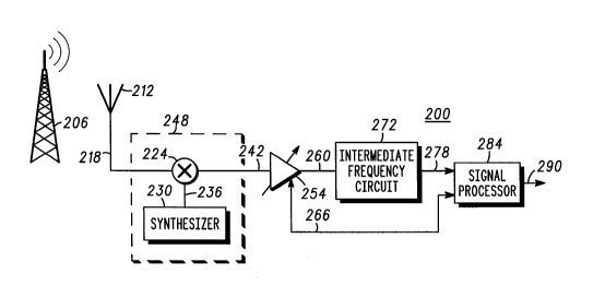
Turning now to FIG. 4, the system of the present
invçn~;o~ efelle~ to generally by lefelence numeral 200, is shown
in simplified block form. System 200 is operative to quickly and
accurately meA~llre the signal level of a signal transmitted thereto.
5 ~erAnce of the speed at which system 200 is able to determine
accurately a signal level of a signal transmitted thereto, a
deter..-;,.~t;on of the signal level may be obtA-ine~l during the IDLE
portion of time period 170 of FIGs. 3A-3B.
A signal trans,~il,~d by a base ~t~t;oA., in-lir~te-l in FIG.
4 by tower 206 is ~celved by ~nt.~nn - 212. ~nt-nn~ 212 generates a
signal indicative of the signal rec~ved thereat on line 218 which is
supplied as an input to miYer 224. A signal generated by frequency
synt~ea~7er 230 on line 236 is rd~litionally supplied as an input to
mixer 224. (The signal generated by frequency srt~esi7er 230 may
5 be altered in frequency to select thereby the frequency rh~nn~l at
which a ~ece;ver is operative.) MiYer 224 mixes the signal supplied
thereto on lines 218 and 236, and generates a mLsed signal on line
242. Mi~er 224 and frequency synt~e~;7er 230 is illustrated to in~liç~te
down-miYin~ in frequency of the signal leceived by ~nt~nn~ 212. It is
20 to be understood, of course, that the down-miYing in frequency
ye.fol~ed by mi er 224 and frequency srt~e~i-7-er 230 typically forms
a portion of more elaborate circuitry forming ~ecaiver down-
collvel~ion circuitry, inrli~te-l in the Figure by block 248, shown in
hatch. Ay~l~o~r;ate c;~c~ r" well known per se in the art, may be
25 1~ i7e'l to for_ a~ yr;ate circuitry to generate a signal of a desired
frequency on line 242.
Line 242 is coupled to an input of variable ~mplifier 254.
~mplifisr 254 generates an Qmplified signal on line 260 which is of a
level, relative to the level of the signal supplied to the ~mplifisr on
30 line 260, which is dependent upon the coeffi~ient value of the gain
coefficiçnt of ~mplifier 254. The gain coefflcient of ~mplifier 254 is
206927~
controlled by a control voltage for_ing a voltage signal generated on
line 266 which is applied to control termin~l~ of ~mplifier 254.
Line 260 is collple~l to interms~ te frequency circuit 272
which is operative to down-conve. l further the signal supplied
5 thereto on line 260, and to generate a down-converted signal on line
278 (~efel~ed to as a b~eb~n~l signal). ~ypically, interme~ te
frequency circuit 272 is ~ pose~l upon an integrated circuit. As
m^nt;or~ previously, the dynamic range of active comro
forming the integrated circuit is limited. Therefore, the signal
supplied to circuit 272 on line 260 must be within the dynamic range
of circuit 272 for circuit 272 to generate a signal of a signal level
which is accurate and .~.e3cnt~t;ve of a signal applied thereto.
When a signal generated on line 260 is beyond the dynamic range of
circuit 272, the signal generated on line 278 is erroneous and is either
5 "clipped" or of a predetermined magnitude.
Line 278 is coupled to signal processor 284 wbich
proces~es the signal supplied thereto on line 278 and generates a
signal in~iic~tive thereof on line 290. Additionally, signal ~locessor
284 ~l,c~ates a signal fo~ , the control voltage on line 266 wbich
20 is o~elslive to control the coeffirient value of tbe gain coefficient of
va~iable ~mplifier 254.
Operation of the circuit fol~ ~y~tem 200 may perhaps
best be described in connection with the grs~p~ir~l repregent~tiQnq of
FIGs. 5A-5C. With r4~ t, tben, to FIG. 5A, the vertically-e~ten~
25 line wbich forms a~is 340 r~e3cnts the pos~ihle signal levels of a
signal ~ece;~l by ~nt~nn~ 212 of ~y~l~ 200. The range of values of
signal levels of ~ign~ls r~eived by ~ntsnn~ 212 e~ten~l bel-. een a
noise level (a signal must be of a level greater than the energy level of
bac~lou"d noise) and a strong ~ignal which is of a signal level
30 r~qull;ng no ~mplifiç~tion (or even ~ttenl)~tiQn) by ~mplifier 254.
Signal spike 350 is repre~ent~tive of a signal transmitted
by a transmitter upon a frequency rh~nnel~ received by antenna 212
2069278
- 13-
of the circuit of system 200, and generated on line 260. Spike 350,
while in~lic~tive of a single frequency, i8 rctv~lly ~e~c3entative of a
modulated Bigllal having a mo~ lption ~ec~r~ Pn~lngous to lines
162 of FIG. 2. Spike 350 iB of a signal level having a value greater
than the energy level of background noiee. A range of energy levels
in~iirPt~ by bracket 360 rlo!fining an upper bound level, in-3ir~tetl by
line 364, and a lower bound level, in~lirPte~l by line 368, ~l,le~ents the
dynamic range of interme li~te frequency circuit 272. A signal
~-lpp~ to circuit 272 on line 260 must be within the dynamic range
thereof for a signal in~lic~tive of the true value of the signal level
thereof to be generated on line 278. As the signal level of signal 350 is
of a value less than the value ~l^fining the lower bound level of the
dynamic range, in~lic~tetl by line 368, a signal supplied to circuit 272
on line 260 of a signal level co.~e~ ;ng to the signal level of line
350 is not accurately e~ l--ce~l on line 278.
FIG. 5B is simil~r to that of FIG. 5A and includes
Rimil~rly nllmhered asis 340, spike 350 le~c3ent~tive of a signal
.e~;ved by ~Pnt~nn~ 212 of the circuit of the system 200, and bracket
360 le~es~n~ing the dynamic range of intermediate frequency circuit
272. The ly~ic range is bounded by an upper bound level,
in-iirPta~l by line 364, and lower bound level, in~iir~t~l by line 368.
FIB. 5B differs from that of FIG. 5A in that the values iefining the
upper bound level and the lower bound level, intlic~te l by lines 364
and 368, .e&~ ;vely, are of different values. T_e dynamic rpnge~
l~c~nte 1 by bracket 360, ho~ e~er, is of the same magnit~ e~ The
upper and lower bound levels ~lefining the dynamic range of circuit
272 are altered by altering the coeffir~ent value of the gain coçffi^içnt
of variable ~mplifier 254.
FIG. 5A i8 f~leeç..~*ve of no ~m~lificp~ion by
~mrlifier 254; FIG. 5B, collvelsely, le~le3ents incremsnt~l increase
of the ~mrlifir~ion of ~mrlifier 254 (i.e., the co~ffici~snt value of the
gain coqffi~çnt of ~mrlifier 254 is greater than one). Such increase
2069278
- 14-
in the ~mplifica*or~ of ~mplifier 254 is indicated by arrow 378. FIG.
5B, ~;mil~r to FIG. 5A, again let)lesents a signal leceived by antenna
212 of the c ;~ of system 200 which is not within the dynamic
range of circuit 272.
The le~r~ornt~t;Qn of FIG. 5C is ~imil~qr to those of
FIGs. 5A-5B, and includes ~imil~qrly-number axis 340, line 350
loaent~t;ve of a signal received by ~ntenn~ 212 of the circuitry of
system 200, bracket 360 represent~t;ve of the d~ic range of circuit
272 which ~l9firleE upper and lower bound levels in~lic~t~l by line 364
0 and 368. The coeffir~ant value of the gain cosffirient of ~mplifier 254
is further increme~t~lly increased relative to the level of
~mplific~t;on of gmplifier 254 shown in FIG. 5B; such increased
~mplific~3tion is in~lic~t~ 1 by arrow 384. Responsive to such
increased ~qmplifir~t;on~ the values ~ ning upper and lower bound
levels in-lir~t~tl by lines 364 and 368, respechvely, are
correspon~lingly altered.
FIG. 5C represents ~mplific~tion of levels such that the
signal level of the signal lcce;ved by ~nt*nn~ 212 of the c.lcuill~ of
system 200 is within the d~llh~c range of circuit 272. Such is
in~ir~ts~l by bracket 390. As the signal level of the signal in~lir~tq~l by
line 350 is greater thsn the level ~1efinsd by the lower bound of the
dynamic range, an accurate determin~tion of the signal level msy be
calc ll~te~l ~e~o~ive to measurement of the magnitude of the signal
within the dynsmic rsnge (such level being indicated in FIG. 5C by
brscket 390) snd the determin~t;~n of the level of s~mrlific~tin-l of
amplifier 254 (in~ te i by the figure by arrow 384). An a~ ,l;ate
algorithm e~ ;e l in signsl proce~sor 284 l~ellllits c~lc~ t;on of
the signal level of the signal ~pplie~l to sntenna 212 when the signsl
level is within the dynamic range of circuit 272, as illustrated in FIG.
5C.
The graphical representation of FIG. 6 inrlic~tes
gr~phi~lly the relationship between the control voltage applied to
2069278
AmplifiPr 254 on line 266 and the signal generated by circuit 272 on
line 278. More particularly, the top portion of the graphical
lcyl~Rçnt~t;on of FIG. 6 plots the magnitude of the level of the control
voltage, VCtl, as a fi)nCtiQn of time, to form plot 410. The control
s voltage, VCtl~ represents the voltage of the signal applied on line 266 to
Amplifier 254.
The hottom portion of FIG. 6 is a plot of the energy level
(i.e., the signal level of the signal generated by circuit 272 on line 278,
as a filncti~n of time, to form plot 420).
min~tion of plot 410 in-lic~At~s an incremQnt~l
increase of the control voltage to form thereby a step filnct;Qn having
a stepped increase of a predetermined rate and of a predetermined
magnitude of increase. More particularly, signal processor 284
generates a voltage signal on line 266 of levels correspon~ling to plot
5 410 of FIG. 6 until the magnitude of the signal sllpplie~ to the
yiOCeB30r 284 on line 278 reaches a predeter~ ,ed value. Such
predetermined value is in~iir~te~l by arrow 424 of the envelope formed
of plot 420, and in~licAte l by threshold voltage level Vt.
When this signal generated on line 278 is of a level
20 collespon-ling to the threshold voltage level Vt, the voltage level of the
signal generated on line 266 by signal y, ocessor 284 decreases by a
predetermined amount, in~liçAte~ in the Figure by bracket 430. Such
decrease in the voltage level of the signal generated on line 266, when
applied to the control termin~ls of AmplifiPr 254, causes a reduction
25 in the coçffiripnt value of the gain coeffi-~iPn~, and, hence, a re-lnc~ion
in the AmplifiCAt;Qn of the signal generated on line 260. Ho.. t ~er,
becAll~e of an intrinsic delay A~so~iAte~i with circuit 272, this
re~ ;on in the level of ~mplificAt;on of the signal gener_ted on line
260 does not cause a decrease in the value of the signal generated on
line 278 for a time period intlil-~te-3 by arrows 440. Thereafter, the
signal level of the signal generated on line 278 is reduced, as
inrlirAts-l by plot 420.
206'927~
- 16 -
The decrease in the voltage level of the signal generated
on line 266, as in-lir~te l by bracket 430, permits a most rapid
dee,ea~c of the signal level of the signal generated on line 278 to
minimi7~ thereby the a O~lllt of time required to accurately calculate
5 the signal level of the signal Ic~;v~d at antenna 212 of the ~,. .lil,l ~ of
the system 200, and as described with .e~*~ to FIG. 5C hereinabove.
The intrinsic delay of circuit 272 may be predetermined,
or is readily me~stl~able, such that the delay period, as inrlic~te~ by
al~o~ 440, is of a known value. Additionally, the relAtiQn~hip
0 between the coeffirient value of the gain coefficient of zqmplifier 254
and the level of the control voltage, VCtl~ may ~imilArly al~o be
predeterminecl, or be readily measurable.
For in~t~nre~ the gr~phic~ ,.eEentation of FIG. 7 is a
plot of the rel~tJo~al~ip bel,. __.1 the gain of the ~mplifier and the
s control voltage, V~l, wherein the value of the gain is plotte 1 on
ordinate a~s 460 as a filn~iQn of the control voltage, VCtl~ on ~hsrissA
axis 470. Plot 480 illustrating the rel~tiQn~hip tLelebelween may be
stored, for e~ ,le, in a mamory look-up table, or m~y be
m~t~^mAtir~lly-described such that the ~csori~tion between the gain
20 of ~mplifier 254 and the level of the control voltage ~p}?lia~tl to control
termin~qls thereof on line 266 is readily kno vn.
Utili7~tion of these known values _ay also be lltili7e~1 to
detel ~le the decrease, in~lir~ts~l by bracket 430, of the control
voltage, VCtl~ applied to the control terminAl of ~mplifier 254.
25 P~er~ e the dec~easc of the control voltage is not i~cle~pnt~l~ as was
the increase, a minim~l amount of time is laq~ ed to determine the
signal level of the signal 1 ec~ived by ~ntrann~ 212.
Turning now to the block diagram of FIG. 8, a radio
telephone lefellcl to generally by lefer~,lce numeral 600,
30 constructed according to the present invention and including
~ of s~ 200 of FIG. 4, i8 showrL Radio telephone 600
includes the c;l~ of system 200 of FIG. 4. Radio telephQne 600
2069278
may, for ç~mple co~;se a portable or mobile radio t~lephQne
lltili7e 1 in a cellular, co ~ iC~tiQn system A signal kansmitted
by a ba~e st~t;~n, in~ir~te~l in the figure by tower 602 is reoeived by
~ntqnn~ 606 ~ntqnn~ 606 ~.le.ates a signal on line 608 which is
co~pl~ to filter 612. Filter 612 filters the l~oe;ved ~i~n~l, and
generates a filtered signal on line 618.
Line 618 is co~lple~ as an input to miser 624 w_ic_ also
~ece;~e~ an osc~ ng signal on line 630 formed by frequency
8rt~ ^E;7er 638 responsive to the oscill~ting frequency of refe~ehce
0 osr~ tQr 646, the oscill~tine signal generated thereat being
connect~l to srt)~si7er 638 by line 652 Miser 624 C~jllV~ ls
downward in frequency the signal supplied thereto on line 618, and
generates a down co-l~,e. led sigDal on line 658 which is s~pplie~ to
filter 664. E ilter 664 generates a filtered signal on line 672 which is
supplied to second miser 680.
Miser 680 ad~lit;~n~lly l~oe;ve8 an osc~ t;~g input
signal on line 686 supplied by oscill~r 692. The 08~ t;ne
frequency of osc~ tQr 692 is controlled by the osrill~1;ne frequency of
l~fe.~oe os~ t~r 646, and is co ~ to osr~ tQr 646 by line 698
Miser 680 ~le.ates a seco~ , down~,llve-led signal on line 704
which is s~l~plie 1 to filter 710. Filter 710 generates a filtered signal
on line 742 which is supplied to vanable ~ ~Jl;r~çr 754 ~mplifier 754
of FIG. 8 co .~ ~I?onds with variable ~mplifier 254 of FM 4. The
coqffi~çnt value of the gain co~ffi~i~nt, and, hence, the level of
~mplifi~;on of the A~ ~l;r.e~l signal generated thereby on line 760, is
oouholled by the voltage level of a voltage signal generated on line 766
and applied to the control termin~l~ of ~mplifier 754. Line 760 is
coupled to interm~ te frequency circuit 772 which generates a
b~q~eb~nd signal on line 778 T ine 778 is co~ple~l to signal p~ce~330r
784 Signal p,~ce330r 784 ~for~s fimctjon~ including signal
leco~ling and speeirh deco ~ g Signal processor 784 is additionally
operative to generate a voltage signal which is sllpplie~l on line 766 to
2069278
- 18-
the control t~ -o-l~ of ~mrlifier 754. Signal proc~ssor additionally
generates a signal on 790 which is suppliet to spe~lrer 796.
A transmit portion of radio telephnn? 600 includes a
transtucer, such as microFh~ - e 830, which cG~ve~ 1,8 a voice signal
into electrical form and generates a signal indicative thereof on line
836. Line 836 is coupled to speerh coter 842 which co,lve, ls the
electrical signal s~lpplie l thereto into a desired, binary sequence, and
generates a signal in~lir-o-t;ve of such on line 848. Line 848 is co ~ple
to enaxler 854 which generates en^o~e~l signal on line 860 which is
0 sl~ppli~d to filter 866. Filter 866 generates a filteret signal on line 872
which is coupled to an input of miser 878. Miser 878 is additionally
coupled to frequency srthe~i~ef 882 by line 886. Frequency
srtll~r7er 882 is coupled to rtfe,e~ce os~ille-tQr 646 by way of line
886. Miser 878 generates a mised signal on line 890 which is filtered
by filter 894. Filter 894 generates a filtered sign~l on line 898 which is
coupled to ontenn~ 606 to ~r.LIi~ tron~mi~8;Qn of an informPt;Qn
signal therefrom.
During those portions of a time period, lefe~.,ced by
,efe,e~ce numeral 170 of FIGs. 3A-3B, the leCeive~ portion of radio
t~lerh~ne 600 is operative to tune-offfrequency by a~,ol";ate
adjllP~m~nt, of frequency srt~e~;7er 638 to detect a signal generated
by a base stot;Q" ' ~o~l by tower 602. Signal l.,ocP~sor 784 is
ol,e,ati~e to generate a control voltage which increment~lly increases
in a monner ~imil~r to that described with ~eL~l to FIG. 6, until a
signal generated by circuit 772 on line 778i~ ea~e~s to a
predetel~ed value. Respons*e to detectiQn of such increase,
signal l,.ocessor 784 generates a control signal of a voltage level of
mag~ e on line 766 to decleage the level of ~mrlifi~-~tion
Of ~mplifier 754. Meng-..t ent of the signal level of the signal
tr~n~mittnfl by base station to ~nt~nn~ 606 of radio telP.ph~ne 600 may
thereafter be c~ te~ Signal proçessor 784 may, for inPtonce~
include an algonthm operative to c~ te the following eqll_tif n
2069278
-
- 19-
MRS = aMMS
where:
MRS is the magDitude of the ,~eived signal le~;ved by
~ntqnn~ 606;
MMS is the magnitude of the mQ~lifie~ signal generated
by circuit 772; and
is the coçffi~iPnt value of the gain coqffirient of
Qmplifi?r 752, as detel"~ ed by the voltage level of the control signal
~pp~ to control termin~lR thereof on line 266.
0 Finally turning now to the flow diagram of FIG. 9, the
method steps of the method of a ~ fel~od emboAimçnt of the present
invention are listed. First, and as in~lic~tetl by block 920, the signal
~ecei~,ed by a f~C~ ef is ~mp1ifie~ to form thereby an PmplifiPd signsl
having a signal level of a value depen~l~nt upon a c~effici~nt value of
a gain coefficient. Nest, and as in~ P.t~l by block 926, a mollifie~
signal i8 generated responsive to the ~mp1ifie~l signal when the
~mp1ifie~1 signal is of a sign~l level within a dynamic range. Next,
snd as in~lic~t~l by block 932, the gain coçffiriPnt de~el..-;..~;ve of the
value of the ~ml~lifie~l signal is incrçmPnt~lly increased when the
20 ~mrlified signal is of a ~ignal level beyond the dynamic range, or
when the signal level of the mo~lifiell signal is of a value less than a
predetermined level. Nest, and as in-lic~tell by block 938, the gain
coeffiriçnt i8 decreased once the signal level of the mn~lifie~l signal is
at least as great as the predetermined level. Finally, and as in~lic~te i
25 by bloclc 944, the signal level of the signal l~CC;v~ by the lec~;ver is
te l responsive to measul~ment of the signal level of the
m~ifi^ l signal and of the coçffi~çnt value of the gain coçffi~çnt~
While the present invention has been described in co- n?cti~n with
the ~ fell~d e~bo~l;m^nt~ shown in the various figures, it is to be
30 understood that other ~!imil~r çmbo~lim^-lt9 may be used and
mo~lifi~t;on~ and additions _ay be made to the described emho~3imen
for lJelfor~lg the same fi~nCt;on of the present invention without
2069278
-
- 20 -
denating the~ce~o Thelefo~e, the present i~ elltion should not be
limited to any 8in~e çmhotlim^nt~ but rather construed in b~ tl and
scope in accordanoe ~nth the recitation of the app~n~^ i cl~im~.