Note: Descriptions are shown in the official language in which they were submitted.
W~ 91/07519 P~'dlUs9~~~6~t~9
s
rr, , a
1..5"'
METHOD FOR COATING SUBSTRATES
WITH SILICON BASED COMPOUNDS
;.
Background of the Invention
This invention relates generally to a method
of forming a film of dielectric material on a substrate,
and more particularly to a technique for depositing
films of silicon based compounds on substrates by
reactive magnetron sputtering.
Silicon compounds, particularly silicon
dioxide (SiOZ) play an integral part in current
materials technology. For example, Sio2 is utilized as
a final protective coating on films that are subject to
corrosion or abrasion, or as a layer material for
multiple film structure. Typical applications include:
architectural and automotive solar-control glass,
mirrors (first- and second- surface), enhanced mirrors,
barrier films (moisture and gas), electronic components,
anti-reflection films and semiconductor devices.
' Various processes are available far applying
silicon based compounds onto substrates. For example,
semiconductor wafers are coated in diffusion operations
at high temperatures of over 1,000°C: However, because
diffusion furnaces use radio frequency ("RF") power, the
size and efficiency of these furnaces are severely
limited. Other semiconductor processes including
thermal oxidation and LPCVD (low pressure chemical vapor
deposition) suffer from, among other things, slow
deposition rates.
WO 91107519 PCT/U~90/46459
:::n~
::;..
. ~ . ..
.. , 2
In addition, there are silicon oxide coating
methods commonly referred as to "wet, dip and dry"
methods for large-scale applications, including glass
and antireflective coatings. However, these methods are ,
inadequate f.or applications requiring high purity and
precise, uniform film thickness on large scale
substrates.
Reactive sputtering techniques have also been
used to form silicon-based compound films. Sputtering
is the physical ejection of material from a target as a
result of ion bombardment of the target. The ions are
usually created by collisions between gas atoms and
electrons in a glow discharge. The ions are accelerated
. into the target cathode by an electric field. A
substrate is placed in a suitable location so that it
intercepts a portion of the ejected atoms. Thus, a
coating is deposited on the surface of the substrate.
In an endeavor to attain increased deposition
rates, magnetically enhanced targets have been used. In
a planar magnetron, the cathode includes an array of
permanent magnets arranged in a closed. loop and mounted
in a fixed position in relation to the flat target
plate. Thus, the magnetic field is caused to travel in
a closed loop, commonly referred to as a "race track",
which establishes the path or region along which
sputtering or erosion of the target material takes
place. In a magnetron cathode, a magnetic field
confines the glow discharge plasma and increases the
length of the path of electrons moving under the
influence of the electric field. This results in an
increase in the gas atom-electron collision probability.
This leads to a much higher sputtering rate than that
which is obtained without the use of magnetic
confinement. Further, the sputtering process can be
accomplished at a much lower gas pressure.
WO 91/07519 R~/~~~~/~~'~
~~,y~~a~..~"~~
3
In operation, the magnetic confinement of the
plasma results in a high rate of erosion of the target
. along the narrow "race track". As a result, only a
relatively small portion of the total target material in
the race track region is consumed before the target must
be replaced. In addition, with planar magnetrons,
limited heat transfer and arcing have also imposed
constraints on the choice of target materials arid power
levels. Arcing and the spitting of debris are problems
associated with silicon oxides since they form good
dielectrics. Major sources of arcing in a planar
magnetron are the edges and the center of the target.
Material deposited in these regions acquires a charge
and arcs as its dielectric breakdown voltage is
exceeded.
In reactive sputtering, a reactant gas forms
a compound with the material which is sputtered from the
target plate. When the target plate is silicon, and the
reactive gas is oxygen, silicon oxide, usually in the
form of SiOZ, is formed on the surface of the substrate.
However, because silicon oxide is such a good insulator,
a film thick enough to cause arcing is rapidly formed in
areas of the target plate outside of the race track.
Silicon oxide is known to be one of the hardest
dielectric films to deposit by magnetron reactive
sputtering,. because of this characteristic. The arcing
associated with silicon oxides has prevented planar
magnetron reactive sputtering from being efficiently
utilized to deposit quality silicon oxide films.
Numerous attempts have been employed to
overcome such arcing .problems and to find a better way
to deposit silicon oxide films. A great deal of effort
has gone into improving planar magnetron reactive
sputtering techniques for depositing silicon oxide and ~.
other films with a high degree of electrical insulation.
Radio frequency (RF) power has been used instead of
CVO 91/07519 PGT/LJS90/06459
direct current (DC) potential in order to reduce the
electrostatic build-up on the target surface. However,
this has the concomitant effect of reducing the rate of
deposition on the substrate as.well. Also, the high ,,
magnitude of ~F power that is necessary for large scale
industrial coaters requires the use of an enormous power
supply, and it is extremely difficult to avoid
generating a level of radiation in the surrounding
. environment that interferes with electronic equipment.
As another technique;,baffles have been employed for
shielding the areas of the target where the troublesome
dielectric film forms. Further, the reactive gas has
been confined to an area adjacent the substrate surface
in order to attempt to minimize the amount of film
deposition molecules that are permitted in the region of
the target surface. Although these approaches have
improved the process to some degree, they have not
yielded a commercially practical technique, particularly
for large scale industrial applications.
Therefore, it is a primary object of the
present invention to provide an improved method of
forming films of silicon based compounds on various
substrates.
It is another object of the present invention
to provide a magnetron reactive sputtering technique for
depositing films of dielectrics with a high electrical
insulating property without suffering the disadvantages
discussed above.
Summary of the Invention
These and additional objects are accomplished
by the present invention, wherein, generally, a rotating
cylindrical magnetron is used for depositing silicon
based compounds, particularly a silicon oxide, and other
good insulating dielectrics, by DC reactive sputtering.
WO 91/07519
PCf/IJ~9~/~~59
The concept of a rotating cylindrical
magnetron is generally known. Tn such a device, a
cathode target assembly in the form of an elongated,
cylindrical tube carries a layer of material applied 'to
5 its outer surface that is to be sputtered. The target
tube is rotated about its longitudinal axis. A magnetic
structure is arranged inside the tube but does not
rotate with it.
What is surprising is that deposition of the
heretofore. very troublesome dielectric films,
particularly silicon dioxide and other silicon based
compounds, is accomplished in this manner without
formation of a layer of dielectric on the target surface
that is thick enough to cause arcing. The apparent
reason is that rotation of the target surface through
the stationary plasma sputters the top layer of material
from substantially its entire surface as that surface is
rotated through the magnetic field. Any dielectric that
is deposited on a portion of the target surface as it
rotates outside the region of the magnetic field is
apparently removed by sputtering when it again passes
through the field. Thick layers of dielectric do not
form, thereby reducing arcing. This.phenomenon may be
referred to as a "self-cleaning" characteristic of the
rotating cylindrical magnetron. Furthermore, DC
potential can be used in a rotating cylindrica l
magnetron, and at high levels because of superior
cooling of the rotating cathode, thereby achieving high
deposition rates. The invention is capable of precisely
depositing silicon based compounds on large substrates.
Additional objects, advantages and features of
I the present invention will become apparent from the
following detailed exemplary description, which
description should be taken in conjunction with the
accompanying drawings.
WO 91/07519 PCT/IJ59D/06459
'i
6
Brief Descri tion of the Drawin s
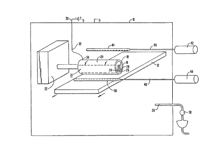
Figure 1 is a schematic representation of a
rotating cylindrical magnetron sputtering system far
deposition of dielectric films according to the present ,
invention; ,
Figure 2a and Figure 2b are each a cross-
sectional view of a cathode assembly;
Figure 3 is a graph of Taber score vs.
thickness of a Si02 overcoat produced with the inventive
method;
Figure ~ is a graph comparing the percent
reflectance of glass coated with a multi-layer Si3N4 and
Si02 film with the percent reflectance of 'uncoated
glass:
Figure 5 is a graph illustrating the percent
reflectance of glass coated with a multi-layer film of
Si3N4 and Si02, burnished and unburnished;
Figure 6 is a graph. comparing the percent
reflectance of glass coated on both sides with a multi-
layer film of Si3N4 and SiOz, burnished and unburnished;
and
Figure 7 shows the percent reflectance of a
mufti-layer coating consisting of Al-Sio2-TiOZ-Sioz-Tio2
films over the visible spectrum of light.
a= 25 Description of Preferred Embodiments
The method of the present invention will be
explained with respect to implementing the rotating
cylindrical magnetron that is generally illustrated in
Figure 1. A plasma is formed in an enclosed reaction
chamber 10, in which a vacuum is maintained, where a
substrate, such as substrate 12, is placed for
depositing a thin film of material upon it. The
substrate 12 can be any vacuum compatible material, such
as metal, glass, and some plastics. The film can also
.., . 3 5
~u~~~r~-~ a r ~ ~~~~~r
V6'O 91/07519 PCf/US90/06459
.~.;:~.,; ~.. :~.
be deposited over other films or coatings that have
previously been formed on a substrate surface.
The cathode assembly 14 comprises generally an
elongated cylindrical tube 16 mounted in the reaction
chamber 10. An elongated magnet assembly 18 is carried
within a lower portion of the tube 16, extends
substantially its entire length, and is restrained
against rotation with it. In order to be able to
operate at high electrical power levels, desireable in
order to have a high film deposition rate, the tube 16
is preferable cooled by passing water or another heat
transfer fluid through it.
The tube 16 is formed of a suitable non-
or
magnetic material such as, for example, brass
xa
stainless steel, and is of a diameter, wall thickness
and length required for a particular operation to be
performed. Applied to the outer surface of the tube 16
is a layer of a selected target material 20 to be
deposited onto the substrate 12 being coated. In order
to deposit a silicon based film on the substrate 12,
this target material is pure silicon that is doped with
a small percentage of a conductive material, such as
aluminum, boron, antimony, phosphorus or arsenic, in
order to render the target surface electrically
conductive. The amount of dopant can be as high as
approximately 100, although less than 6% is better. The
preferred amount is approximately as near zero as
possible while achieving the necessary electrical
conductivity. A concentration of approximately 2% is
practically achieved by plasma spray techniques. The
target material 20 is preferably applied to the core
tube 16 by plasma spraying. Thus, the tube 16 and the
layer of coating material 20 constitute a tubular target
or sputtering source as distinguished from the
convention planar target.
W~ 91/07519 P~Cf/US90/06459
a~~,''~~~~~
8
The tube 16 is supported in a manner to be
rotated about its longitudinal axis by a target drive
system 22. The orientation of the longitudinal axis
depends upon the shape and position of the substrate ,
that is being coated. 2n the example being described
herein, the substrate 12 is held horizontally and is
flat, and the longitudinal axis of the tube 16 is also
horizontal, thus being parallel with the substrate
surface to be coated.
Tn a preferred arrangement, somewhat different
from the schematic representation of Figure 1, the tube
16 is rotatably held at each end in a horizontal
position. A support structure at one end also allows
cooling fluid to be introduced into the tube 16 and
withdrawn from it, and contains a mechanism for driving
the tube 16 from a motor source outside of the vacuum
chamber 10. Rotating seahs are included in this support
structure for isolating the cooling fluid from the
vacuum chamber. A support structure at an opposite end
includes an electrical brush assembly for connecting the
tube to a negative voltage.
The magnetic assembly 18 comprises an array of
magnetic poles arranged in straight parallel rows along
the length of the tube 16. Each row has three
alternating magnetic poles 24, 26 and 28. In one
configuration, the poles 24, 26 and 28 are arranged to
have respective north, south and north polarities. An
opposite configuration of respective south, north and
south polarities may also be used. In either case, the
magnetic poles 24, 26 and 28 are positioned in relation
to the tube 16 so that their lines of force run from one
pole, through the tube 16, and.back through the tuba in
a curved path to an adjacent pole having an opposite
polarity. This arrangement generates what is called a
which not only allows the sputtering
netic tunnel
ma
,
g
rate to be increased, but also causes the target
WO 91/07519 PGT/LJS90106459
9
material 20 to be removed faster inside the tunnel,
especially in the middle of this magnetic pattern.
The arrangement of the magnetic assembly 18 in
Figure 1 is a "W" configuration of three elongated
magnets 24, 26 and 28. An alternative is a 'U"
configuration wherein a single magnet is position in the
middle and a "U" shaped piece of magnetic material is
positioned to form poles on either side of the magnet
and of opposite polarity. In either case, it is usually
desireable to position the pole faces as close to an
inner surface of the tube 16 as possible. The magnetic
assembly 18 is preferably supported within the tube 16
from a .stationary axial rod or cooling fluid tube, or is
held away from the inner surface of the tube 16 by
rollers that are carried by the magnetic assembly 18, or
both.
A cathode potential V sufficient to cause
sputtering to occur is supplied to the tubular target 20
from a DC power source 30 through a power line 32 having .
sliding contact 34 with the tube 16 by a conventional .
electrical brush. The enclosure of the reaction chamber
10 is conductive and electrically grounded. It serves
as an anode in the sputtering process. A separate anode
may be optionally employed and maintained at a small
positive. voltage. Such an anode is a plane positioned
above the target tube surface 20 and is preferably water
cooled in order that high power levels may be employed.
In order to obtain the low pressure necessary
far the coating operation to be performed, the reaction
chamber 10 is provided with an outlet tube 36
communicating with a vacuum pump 38.
In order to provide the chamber 10 with the ,
gases necessary for the coating operation, a gas supply
system is included. A first gas supply tube 40 extends
into the coating chamber 10 and from a source 42 of an
inert gas. The inert gas is preferably argon for the
W~ 91/07519 PCT/CJS9~/06459
specific methods being described. Nozzles 44 connected
to inlet tube 40 distribute the inert gas in a region .
above the rotating cathode 14. It is the inert gas that
breaks down into electrically charged ions under the ,
5 influence of.an electric field established between the
target surface 20 and the grounded chamber enclosure or
separate floating anode. The positive ions are
attracted to and bombard the target surface 20, under
the influence of the electric field, in an area to which
10 they are guided by the magnetic field. This bombardment
occurs primarily in two parallel strips, one between
each of the opposing magnetic poles, along the length of
the cylinder 14 at its bottom, opposite the magnet
assembly 18. Thus, as the tubs 16 is rotated, its
target surface 20 is rotated through these two parallel
strips.
A second gas supply tube 46 extends through
the coating chamber 10 from a reactive gas source 48.
' When an oxide film is to be deposited, such as silicon
oxide, the reactive gas is chosen to be pure oxygen. If
a nitride film is to be deposited, such as silicon
nitride, the reactive gas is chosen to be pure nitrogen.
To form a silicon carbide film, the reactive gas is
selected from hydrocarbon gases. Nozzles 50 connected
to inlet tube 46 distribute the reactant gas close to
and across the width o,f the substrate 12 being coated.
Molecules of the reactive gas combine with molecules
sputtered from the target surface, as a result of ion
bombardment, to form th~ desired molecules that are
deposited on the top surface of the . substrate 12 . Thus,
silicon oxide films are deposited by use of the silicon
material cylindrical target surface 20 and oxygen as the
' reactive gas. '
Many variations in the gas supply system shown
are practical as well. The inert and reactive gases
from the sources 42 and 48 can be combined and delivered
WO 91/07519 ~'~'f/~J~9b~/0~459
j
lw':'vi . . . ,.
11
into the chamber 10 through a common tube and set of
nozzles. When this is done, the delivery tube is
preferably positioned along a side of the rotating
target tube 16 and parallel with its longitudinal axis.
Two such tubes can be used, one on each side of the
target tube 16 and parallel with its longitudinal axis,
each delivering the same combination of inert and
. reactive gases. Also, more than one reactive gas can be
simultaneously supplied, depending upon the film being
deposited. An example is to supply both oxygen and
nitrogen in order to coat the substrate ,12 with a
silicon oxynitride film.
The film being formed does apparently become
deposited on a surface portion of the target 20 after it
leaves the region below the stationary magnetic
structure 18, in the same manner as occurs on a planar
magnetron target surface. But it has been found that
this is no problem because the deposited film apparently
is removed by the sputtering process when that surface
portion again rotates through the region below the
magnetic structure 18. It has also been found that this
removal does not impair the quality of the film formed
on the substrate 12, nor does it impact on the rate of
deposition of the film.
The film is, however, deposited on other
surfaces within the chamber 10 that are maintained at
the large negative potential of the target surface 20.
Such surfaces can exist in the supporting structures of
the tube 16. If they do, it is highly desireable to
cover them with a dielectric so that any deposited films
will not have the large voltage surface immediately
behind them and arcing will be avoided. If a positive
voltage, floating anode is used, its surface is shaped
and pasitioned away from such negative voltage surfaces
in order to draw the plasma away from them and thus
reduce deposition on them.
CA 02069329 2000-O1-25
12
The example of Figure 1 shows a single target
assembly, for simplicity, but it may be preferred to
position two or more such assemblies adjacent each other
with their tube longitudinal axes being parallel. This can
result in an increased rate of deposition. Figure 2a and
Figure 2b each shows a cross-sectional view of a cathode
assembly which together forms a dual system. It may be
preferred, for large scale machines, that the magnetic
poles of adjacent target assemblies which face each other
be of opposite polarity. This restrains the plasma from
extending upward between adjacent target assemblies. In
this embodiment, the magnetic poles alternate in polarity
so that if pole 28 is north, pole 52 is south, or vice-
versa. As described previously, the magnetic field lines
of flux 58 generate a magnetic tunnel wherein the
sputtering is concentrated. Points 60 and 62 denote the
approximate outer boundaries of the tunnel in one assembly
and points 64 and 66 denote the approximate outer
boundaries of the other. Additional structural and
operational details of a rotating magnetron of the type
described with respect to Figure 1 may be had by reference
to U.S. Patent No. 5,096,562 of March 17, 1992.
Experimental Results
The method according to the invention provides
30 durable silicon based compound coatings which can be
deposited at relatively high rates. To demonstrate the
method's effectiveness, films of silicon oxide (Si02) and
Si3N4 were prepared on different substrates and were
tested for their mechanical and optical properties and
deposition rates. It is known that Si02 is the
w W~ 91/07519 ~'~'/~J~~9~/~~59
;;~~z. < . .
13
predominant form of silicon oxide created in 'the
sputtering process. However, it is believed that other
forms are produced as well. Thus, unless otherwise
stated, SiOz will represent all forms of silicon oxide
produced by.the inventive method. In addition, by
utilizing reactive gas mixtures more complex silicon
compounds are sputtered. For instance, when the mixture ~,.
consists of oxygen and nitrogen, SiXO~,NZ is deposited,
where x, y and z represent different stoichiometric
amounts of silicon, oxygen, 'and nitrogen of the various
compounds formed. Furthermore, by regulating the
process conditions, particularly the flow rates of
oxygen and nitrogen and the pressure of the reaction
chamber, x, y and z can be controlled.
Experiments utilizing the inventive method
were originally conducted in a research size in-line
cylindrical magnetron of the type. shown in Figure 1
manufactured by Airco Coating Technology, a division of
Assignee. The same results were later duplicated in a
larger cylindrical magnetron, the C-MagTM model 3000
cathode, also manufactured by Airco under substantially
the same process conditions. In addition, more
sophisticated applications of the inventive method are
possible with the model 3000. The.research coater is
capable of substrate sizes up to 16 inches wide, whereas
the larger coater was capable of substrate sizes up to
1 meter wide. Research coaters normally operate at
approximately 3 kw power whereas the mpdel 3000 normally '
operates between 30 to 40 kw. Tests indicate that the
research and model 3000 produce film of the same
quality. Both systems use entrapped diffusion pumps
that achieved a base pressure in the 10 6 Torr range
before operation. Argon was used as an inert gas and
either oxygen or nitrogen was used as the reactant gas.
The partial pressure of the gases was determined by the
transition from the oxide or nitride mode to the
WO 91/07519
PCT/US9~/06459
> J y-oi~
n
14
metallic mode. Experiments were run as close to that
transition as practicable. The pressure and flow rate ,
of the sputtering gases were controlled by conventional
devices.
The power applied varied for the different
target materials but for the most part it was comparable
to the maximum obtainable with similar size planar
magnetrons. Each sputtering source was connected to an
appropriate direct current power source having provision
for automatically maintaining the voltage, current or
power, as desired. ,
Because the electrical conductivity of pure
silicon is so low that it is unsuitable for sputtering
with direct current, the silicon target was impregnated
or doped with a small amount of aluminum in the range of
from 2-4%. The target was prepared by plasma spray.
The film deposited according to the invention
contains reaction products of aluminum and silicon with
the reactive gas. When the reactive gas was oxygen, the
deposition coating contained a mixture of aluminum and
silicon oxides. It is believed that the percentage of
aluminum oxides in the film is approximately equal to
the percentage of aluminum in the target. The amount of
aluminum oxides increases proportionally with the amount
' 25 of aluminum in the target. When other substances are
used as dopant, a similar correlation between the amount
of dopant in the target and the amount of the dopant
oxide is seen. When the sputtering gas was nitrogen,
the coating contained a mixture of aluminum and silicon
w 30 nitrides. All of these four components are relatively
hard and form an amorphous film that acts as a strong
barrier. However, the amount of aluminum in the film
did not interfere with formation of the desired silicon
based compound films. In the course of the experiments,
35 two silicon compound films were sent out for independent
RBS (Rutherford Back-Scattering) sampling to determine
CA 02069329 1999-08-06
the composition of the compound. The silicon oxide
measured 36% Si/64% O, and the silicon nitride measured
42o Si/57% N. These percentages are very close to the
theoretical 1:2 ratio for oxide and the 3:4 ratio for
5 nitride.
The target was conditioned using an inert gas,
then the process gas was added until the desired partial
pressure was reached. The process was operated at that
point until the process was stabilized. The substrates
10 were then introduced to the coat zone and the film was
applied. The substrate used was typically soda lime
glass, but, depending on the test, could be any
combination of the following: microscope slide, Corning
7059 glass, 0.5 mil PET (poly(ethylene terephthalate))
15 film, fused silica stressed disc or carbon planchet.
Deposition Rate: The deposition rates for the
production of SiOz and Si3N4 utilizing the inventive
method were measured and compared with deposition rates
of other films applying the same process.
Various factors affect deposition rates,
including gas partial pressure, source-to-substrate
distance, system cleanliness, magnet design, and chamber
geometry, which accounts for the range of deposition
rates listed below. For the materials studied, the
dynamic deposition rate (DDR) for the cylindrical
magnetron was similar to, or greater .than, the
equivalent rate for a planar under the same conditions.
Physical thickness of the films was measured
using a Sloan'Dektak IIA Profilometer. The films were
produced by depositing over lines drawn by a permanent
marker followed by delaminating the film over the line
in an ultrasonic alcohol bath. The sputter efficiency,
or DDR, was calculated for each film using the physical
thickness and deposition parameters in the equation
TRADEMARK
W~ 91/07519 PC'T/US90/06459
~~,~~~a ~'~~
16
given by Waits (see R. K. Waits, Thin Film Processes,
page 150, Academic Press, New York, 1978): ,
DDR(hMMZ/Joule)=(d*C*S)/(P*n)
Where: d = Thickness of the film in angstroms
C = Racetrack length of the target in mm
S = Conveyer speed in mm per second
P = Power applied in watts
n = Number of passes.
Below is the typical range of dynamic
deposition rates obtained with the cylindrical magnetron
applying the inventive method:
Film DDR
SiOz 700-1100
Si3N4 900-1400
Abrasion Resistance: The durability of Si02 films and
. , Si3N~ produced by the inventive method was measured with
a Taber Abrader. A CS10F wheel with 500 gram weights
was used. For the standard Taber score the sample was
rotated under the wheels for 50 revolutions. The area
of the abrade was observed through a microscope at 50
times magnification and a picture was taken. Four 1" x
1" squares were drawn on the picture in random places
and the number of scratches inside these squares was
counted. The number of scratches in all four squares
was averaged and the part was given a Taber score based
on the following formula:
TABER SCORE = # SCRATCHES * (-0.18) + 10
The Taber score is a linear scale where no scratches is
a 10, and 50 scratches is a 0. For reference, uncoated
soda lime glass typically scores about 9Ø
Silicon oxide films of different thicknesses
were coated on VWR (Vanwater and Rogers Co.) slides.
The cathode was run at 2.0 kW and the line speed was
dvo 9ieo7si9 pcreus~oeo~as~
,.
~~~ ~u_~..~,
17
2o°'/min. The other operating conditions of the
cylindrical magnetron were comparable to those set forth
in Table 1 below. 4" x 4" samples were cut from each
run for Taber Abrader tests. The results indicate that
a 900 ~. thick sample had a Taber score of 9.40 and a
3000 A sample had a Taber score of 9.70. FTIR analysis
showed the film to be relatively pure and free of
contamination. SEM cross-section analysis showed that
the Si02 was dense and amorphous. '
The following table shows typical Taber scores
for some of the compounds studied:
Cylindrical Magnetron Planar
Compound Taber Score Taber Score
SiOz 9.6 .2 9.55 .2*
Si3N4 r 9.45 .3 9.3 .6*
.
Ti02 8.5 8.5 ~
*The planar silicon compounds were produced using an RF enhanced
system.
Protective Overcoat of Soft Undercoat: A study of the
abrasion resistence of a SiOz overcoat on a very soft
film was done. Super-HR is a solar control, low
emissivity film developed by Airco; it is relatively
soft because it uses metal as one of its layers. By
applying a hard, but relatively neutral film such as
SiOZ, its durability should be improved without
impacting the optical properties. Glass substrates
previously coated with Super-HR were coated with silicon
oxide films of different thicknesses. The cathode was
run at 2.0 kW and the line speed was 20"/min. except for
the 8250 ~, sample where the speed was 2.3'/min. The
other operating conditions of the cylindrical magnetron
were comparable to those set forth in Table 1 below.
The Taber scores for various samples are tabulated as
follows:
WO 91/07519 P~f/US94/0~59
~~~ ?
,ar
SiOZ Thickness yA) Taber Score
uncoated 3.57 ,
445 6.94
1063 7.93 ,
' 5 3000 9.37
8250 9.55
9600 9.76
Figure 3 graphically illustrates the above
results.
Si02 as a Barrier Layer: On a 6" x 6" PET sample, a
3000 h film of Sio2 was prepared. In. this particular
example, during the sputtering process which took 31
minutes; the substrate sample was passed through the
plasma 16 times. Table 1 sets forth the process data
for production of the oxide. Beginning at zero, Time
refers to the lapsed time in the process. The Potential
refers to the potential between the cathode assembly
tube and the ground. The Power refers to the power ,
supplied and the Current was, measured at the power
source. The flow rates of the inert gas (Ar) and
reactive gas (OZ) were measured in standard cubic
centimeters per minute (SCCM). The Pressure of the
reaction chamber is measured in microns. Finally, the .
Number of Passes refers to the number of times the
substrate had crossed the plasma during the sputtering
process at a particular time. For instance, at time 23
minutes into the process, the substrate was making its
13th pass:
"i
TABLE 1
Time Power Potential Current SCCM SCCM Pressure
min -(kWZ (V) _ (A) O~_ Ar (u) No. Passes
0 3.0 481 6.30 10 23 0.98 1
6 3.0 500 6.06 10 23 1.10 4
13 3.0 490 6.18 10 23 0.99 7
CA 02069329 1999-08-06
19
17 3.0 S00 6.14 10 23 1.09 10
23 3.0 503 6.06 10 23 1.05 13
31 3.0 506 6.02 10 23 1.10 16
Total No. of Passes: 16
Water permeation testing was done on a Mocon
Permatran and oxygen testing was done on a Mocon*Ox-Tran
Twin. In one test, approximately 3000 A of SiOz was
applied to a 6" x 6" x 0.5 mil PET sample. This was
- tested for water permeation, an uncoated sample had a
measured transfer of 43.4 grams/Mz/day while the coated
sample only had a transfer of 3.3 grams/Mz/day.
In another test approximately 3000 ~ of Si3N4
was applied to a 6" x 6" x 0.5 mil PET sample. This was
tested for oxygen permeation. At 32°C the uncoated
sample had a transfer of 161.2 cc/Mz/day while the
coated sample had a transfer of 5. 96 cc/Mz/day. At 25 ° C
the uncoated sample had a transfer of 23.89 cc/Mz/day
while the coated sample had a transfer of 4.7 cc/MZ/day.
Optical Characteristics of Plain Si02: A VWR slide
coated with a 8250 A film of SiOZ under similar
conditions as set forth in Table 1 was tested for
various optical and physical characteristics as
tabulated hereinbelow:
Index of refraction at 520 nm 1.46
% Transmittance (integrated D65 source)* 91.98
Reflectance (single surface 3.42
integrated D65 source)**
Absorbance 0.70
(or 8.48 x 10 b % A/A)
* The uncoated slide had a % transmittance of
92.27
** The uncoated slide had a o Reflectance of 3.83.
TRADEMARK
~~ 91/07519
PCT/U590106s159
~ ~.~~
Wide Band Anti-reflective Coating using SiO., and Si~N~ Films:
On a glass substrate, a four-layer coating consisting of ,
alternative layers of Si3N4 and Si02 was prepared. Table
w 2 sets forth the process data for the production of the ,
5 oxide and nitride films. Substrate speed refers to how
fast the sample was passing the plasma.
TABLE 2
Thickness Potential Current Pressure Substrate Speed
Layer (A) (V) _ (A) _ (u) No. Passes (in./min.)
1 0 Si3N4 180 670 2.99 1.18 2 31.6
Si02 250 501 4.00 1.02 3 21.8
Si3N4 1375 670 3.00 1.15 10 20.7
Si02 750 510 3.96 1.07 10 22.9
Curve 68 in Figure 4 is the percent
15 reflectance of the uncoated glass substrate. Curve 70
is the percent reflectance of the mufti-layer film.
Wide Band Anti-reflective Coating using Si02_and Ti02 Films:
On a glass substrate, a four layer coating consisting of
alternating layers of Ti02 and Si02 was prepared. Table
20 3 sets forth the process data for the production of the
oxides.
TABLE 3
Thickness Potential Power Current Pressure Substrate Speed
Layer (A) <V) (kW) (A) (le) No. Passes, (in/min)
2 5 Ti02 130 4b8 40 92 3.0 1 22
Si02 283 364 11.5 32 1.5 1 20
Ti02 1132 465 40 93 3.0 44 120
Si02 8b1 3b5 10 27 1.5 26 160
..' Curve 72 of Figure 5 is the percent
reflectance of the unburnished film. Curve 74 is the
percent reflectance of the burnished film.
After coating one side of the glass substrate
with the oxides as described above, the other side of
WfJ 91/07519 PCT/US90/064159
..
21
the substrate was also similarly coated. Curve 76 of
Figure 6 is the percent reflectance of an unburnished
film. Curve 78 is the percent reflectance of the
burnished film.
EnhancedAluminum Mirrors: On a glass substrate, a five
layer coating consisting of a single aluminum film
followed by alternative layers of Sia2 and Ti02 was
prepared. Table 4 sets forth the process data for the
production of the aluminum and oxide films.
TABLE 4
Thickness Potential PoNer Current Pressure Substrate Speed
Layer (~) (V) ckul (A) _ (~) No. Passes ~ (in/min>
Al 650 512 30 55 1.5 1 88
Si02 797 369 10 28 1.5 25 1b0
1 S Ti02 510 449 40 96 1.5 22 130
Si02 949, 368 10 28 1.5 36 160
Ti02 532 452 40 9b 1.5 23 130
Figure 7 is a graph of the percent reflectance
of the film measured against the wavelength. of radiation
over the visible spectrum. Reflectance was measured at
a six (6) degree angle of incidence.
Although the invention has been described with
respect to its preferred embodiments, it w111 be
understood that the invention is to be protected within
the full scope of the appended claims.