Note: Descriptions are shown in the official language in which they were submitted.
2069378
AE-374 P~TENT
BOARD MOUNTED SHIELDED ELECTRICAL CONNECTOR
~, FIELD OF THE INVENTION:
The present invention relates to an electrical
connector, and more particularly, to a shielded electrical
connector for mounting on a printed circuit board and for
; attachment to a complementary electrical connector.
BACKGROUND OF THE INVENTION:
Right angle D-faced electrical connectors are used
in the electronics industry as an input/output (I/O) device
to interconnect a computer to external peripheral equipment.
i0 The contacts of the electrical connector are typically
soldered to conductive traces on a printed circuit board at
a back wall or panel of the computer. A conductive shell
surrounding the contacts in the housing of the connector is
frequently used as a shield to protect against electro-
magnetic or radio frequency interference ~EMI/RFI). Aconductive locking clip is often used to retain the
connector on the printed circuit board for soldering the
contacts by a conventional wave soldering process. The
locking clip further serves as a means to connect a ground
23 trace on the printed circuit board to the conductive shell
of the connector. The front face of the connector, in
addition to having the D-face for polarization, typically
includes latching structure for mating with a complementary
electrical connector which is attached to the peripheral
equipment.
With respect to such latching structure, as
disclosed in U.S. Patent 4,808,125 (Waters, et al), due to
the prospect of repeated mating and unmating of the right
angle D-connector to the complementary connector, it is
preferable that the latches on the connector be formed of
metal, such as a cast metal, rather than plastic which may
be susceptible to failures. In the Waters, et al patent,
not only the latches, but the entire connector housing is
integrally formed of a cast metal, thus complicating the
shielding of the electrical contacts in the connector.
2069378
1 Individual metal latching blocks, for example, as disclosed
in U.S. Patent 4,506,937 (Cosmos, et al) are also used for
attachment to a mating complementary connector. While
individual latching blocks may be more cost effective and
less complicated than a one-piece housing with latches,
attention must be provided in securing the latching blocks
to the connector in a manner that would properly align its
latches and prevent rotation thereof so that attachment to
the complementary connector may be properly made.
As to the locking clip that is used as a ground
commoning element and as a means to retain the connector to
a printed circuit board during contact soldering, such a
-clip is shown, for example, in U.S. Patent 4,721,473
(DelGuidice, et al). It is noted by DelGuidice, et al that
alignment of the connector on the printed circuit board is
desirable in order to properly interconnect to the mating
complementary connector without placing undue stress on the
circuit board connections. In this regard, the locking clip
typically includes resiliently deformable legs that are
frictionally received in openings in a printed circuit
board. Due to the resistive force accompanying the
insertion of the resilient legs into the board openings, it
is desirable to prevent the locking clip from experiencing
excessive bending that would result in misaligned or
improper mounting of the connector to the printed circuit
board.
SU~ARY OF THE INVENTION:
It is an object of the present invention to
provide an improved shielded electrical connector.
It is a further object of the present invention to
provide a shielded electrical connector having an improved
latching block for attachment to a complementary electrical
connector and an improved locking clip for mounting on a
printed circuit board.
In accordance with a preferred form of the
invention, a shielded electrical connector comprises an
insulator of insulative material including a body and two
2069378
l spaced ear portions, each ear portion projecting outwardly
from the body and comprising a mounting wall and a base. An
opening is formed through the mounting wall. The body has
a plurality of apertures therein supporting a respective
plurality of electrical contacts. A conductive shell is
supported on the insulator body and comprises two spaced
flanges. Each flange has a surface disposed adjacent a
respective insulator mounting wall and has an opening
therethrough in substantial registry with the respective
opening in the insulator mounting wall. The connector
further includes two one-piece, metal latching blocks for
attachment to a complementary electrical connector. Each
block is disposed adjacent a respective flange of the shell.
Each block further comprises a generally flat plate having
opposed surfaces and a latching member projecting outwardly
from one of the surfaces in a direction away from the shell
flange. A bushing projects from the opposite plate surface,
the bushing extending through the opening in the shell
flange and through the opening in the mounting wall of the
ear portion. The bushing has as an internally threaded
aperture opening through the surfaces of the flat plate. A
keying element projects from each block toward a respective
ear portion mounting wall and is engagement therewith for
aligning each block relative to the shell flange and for
providing anti-rotation resistance thereto. The keying
element is spaced from the bushing and is of configuration
lying within the periphery of the mounting wall. Two
conductive locking clips are supported by the insulator
base. Each clip has a securement portion secured to a
respective bushing and a resilient latching portion
projecting outwardly from the base for resilient mounting to
an electrical circuit on a printed circuit board.
In accordance with another aspect of the
invention, a shielded electrical connector comprises an
insulator of insulative material including a body and two
spaced ear portions, each ear portion projecting outwardly
from the body and comprising a base and a mounting wall.
2069378
1 The body has a plurality of apertures therein supporting a
respective plurality of electrical contacts. A conductive
shell is supported on the insulator body and comprises two
spaced flanges, each flange having a surface disposed
adjacent a respective insulator mounting wall. Two one-
piece, metal latching blocks are provided for attachment to
a complementary electrical connector. Each block is
disposed against a respective flange of the shell, and
comprises a latching member projecting outwardly therefrom.
Further included in the connector are two conductive locking
clips supported by the insulator base. Each clip has a
securement portion attached electrically to the shell and a
resilient latching portion projecting outwardly from the
base for resilient mounting to an electrical circuit on a
printed circuit board. The clip further includes means
providing bend resistance upon mounting of the clip to the
printed circuit board.
BRIEF DESCRIPTION OF THE DRAWINGS:
Figure 1 is an exploded, top perspective view of
a shielded electrical connector in accordance with a
preferred embodiment of the invention.
Figure 2 is a front, perspective view of a one-
piece, latching block for particular use in the electrical
connector of Figure 1. Figure 3 is a rear, perspective
view of the latching block illustrated in Figure 2.
Figure 4 is a rear elevation view of the latching
block of Figure 3.
Figure 5 is a cross-sectional view of the latching
block of Figure 4 as seen along viewing lines V-V.
Figure 6 is a rear, perspective view of a locking
clip for particular use in the electrical connector of
Figure 1.
Figure 7 is a rear perspective view of a
fragmentary portion of the electrical connector of Figure 1,
showing details of the connector insulator base on which the
locking clip of Figure 6 is secured.
2Q69~78
1 DETAILED DESCRIPTION OF THE PREFERRED EM~30DIMENTS:
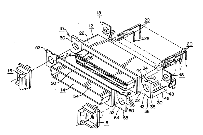
Turning now to the drawing figures, there is shown
in Figure 1 a right angle D-faced shielded electrical
connector 10 for mounting on a printed circuit board and for
attachment to a complementary electrical connector.
Connector 10 basically comprises an insulator 12, a
conductive shell 14, a pair of metal one-piece latching
blocks 16, a pair of conductive locking clips 18 and a
plurality of right angle electrical contacts 20.
The insulator 12 is formed of insulative material,
preferably being a molded thermo-plastic material and
comprises a generally elongate body 22. Projecting
outwardly from the front surface of the body 22 is a nose
portion 24 configured in the industry standard D-
configuration for polarization purposes. Extending through
the nose portion and the insulator body 22 are a plurality
of apertures 26 which open through the front surface and the
rear surface (not shown) of the body 22. In the arrangement
shown, there are two rows of 25 apertures each, each
aperture being spaced 0.05 inch within a row, and the upper
and lower row being spaced 0.100 inch. It should be
appreciated that different numbers of apertures at different
spacings may also be used within the context of the
invention. The electrical contacts 20, each having a right-
angle bend, are received respectively in the apertures 26
and are supported in the insulator body 22. The contacts 20
each include a terminal pin 28 for receipt in openings in a
printed circuit board (not shown) for subsequent soldering
thereto so as to electrically interconnect the connector 10
to electrical circuits on the printed circuit board.
Insulator 12 includes a pair of ear portions 30
projecting outwardly from the respective ends of the body
22. Each ear portion 30 comprises a generally planar
mounting wall 32 defined by an upper edge 34 and a lower
edge 36 that are substantially parallel to each other and an
interconnecting outer edge 38 that is substantially
perpendicular to the upper and lower edges respectively.
~Ofi 9~78
l Bxtending into the upper edge 34 is a curved recess 40 and
extending into the lower edge 36 is a similarly configured
curved recess 42. The upper recess 40 and the lower recess
42 are preferably aligned with each other in a plane
generally parallel to the outer edge 38. As will be
described hereinafter, recesses 40 and 42 provide keyways
for keying the latching block 16 upon assembly of the blocks
16 to the insulator 12. Extending through the mounting wall
32 of each ear portion 30 is an opening 44. In the
preferred arrangement, the recesses 40 and 42 are aligned
closer to the body 22 than is the central axis of the
opening 44. Each ear portion further includes a base 46
extending rearwardly from a respective mounting wall 32,
each base 46 having an opening 48 therethrough for retentive
receipt of a respective locking clip 18 therein.
Referring still to Figure 1, the conductive shell
14 comprises a generally elongate, planar frame 50.
Projecting outwardly from the ends of the frame 50 is a pair
of generally planar flanges 52, each of the flanges being
substantially parallel to the frame 50 and being offset
rearwardly with respect to the frame 50 by a spacing, s.
Extending outwardly from the front of the frame 50 is a
continuous nose section 54 configured in complementary form
to the D-shape nose portion 24 and adapted form surrounding
receipt thereon.
Each flange 52 is defined by an upper edge 56 and
a lower edge 58 that are substantially parallel and an outer
edge 60 that joins the upper and lower edges 56, 58 and is
substantially perpendicular thereto. A curved upper recess
62 extends into the upper shell edge 56 and a lower curved
recess 64 extends into the lower shell edge 58. An opening
66 extends through each flange 52. Upon attachment of the
shell 14 to the insulator 12, the flanges 52 are formed to
lie against the respective ear portions 32, the flange
recesses 62 and 64 being formed to lie in substantial
registry with the recesses 40 and 42 in the mounting wall,
and the flange opening 66 to lie in substantial registry
2Q69378
1 with the opening 44 in the mounting wall. In the preferred
embodiment, the shell 14 is a drawn steel shell which
provides protection against electro-magnetic interference
(EMI) and radio frequency interference (RFI) for the
; contacts supported in the insulator 12. Further, as will
be described, the shell 14 may be electrically commoned to
a ground trace on a printed circuit board by the conductive
locking clips 18.
Turning now also to Figures 2 through 5, the
details of the latching block in accordance with a preferred
form of the invention may be more fully understood. Each
block 16 is formed as an integral, one-piece block of metal,
preferably a die-cast metal, such as zinc. Each block
comprises a substantially flat plate 68 including a front
planar surface 70 and a rear planar surface 72. Each flat
plate is defined by spaced, opposing substantially parallel
side edges 74 and 76 and spaced, opposing end edges 78 and
80. Side edges 74 and 76 together with end edges 78 and 80
define a substantially rectangular shape of flat plate 68.
Projecting outwardly from the front surface 70 is
a latching member 82 defined by a pair of spaced, latching
teeth 84 and 86, each having an inclined outer surface. The
latching teeth are adapted to engage a latch of a
complementary connector (not shown) in snap-action fashion
to secure each of the latching blocks 16 to such
complementary connector. Each latching block 16 may further
include a pair of substantially parallel, spaced ledges 88
and 90 projecting from the front surface 70, each ledge 88,
90 serving as guide members in the attachment to a
complementary connector.
Projecting rearwardly from the rear surface 72 of
each latching block 16 is a pair of keying elements 92 and
94 that are formed to lie within the periphery of the flat
plate 68. Each latching element 92, 94 is respectively
formed to have a keying surface 96, 98, such keying surfaces
being configured for cooperative engagement with the
recesses 40 and 42 in the mounting wall 32 of the insulator
20~937~
1 body 22. In the preferred arrangement, the keying surfaces
96 and 98 are formed to be non-linear and are generally of
semi-circular, curved shape. Adjacent the respective upper
and lower end edges 78 and 80, each keying element includes
a substantially flat surface 100, 102 that are within the
respective end edges 78 and 80 and are substantially
parallel thereto. As illustrated in Figure 4, the keying
elements 92 and 94 lie adjacent the end edges 78 and 80 and
the centers of the keying elements lie in a plane 104 that
is substantially parallel to the side edges 74 and 76.
As seen in Figure 3, a bushing 106 of generally
cylindrical outer configuration projects outwardly from the
rear surface 72 of each latching block 16. As seen further
by reference to Figure 5, the bushing 106 includes an
internally threaded aperture 108 that opens through the
front surface 70 and the rear surface 72. At its rearward
distal end, bushing 106 includes a relatively thin wall 110
that is particularly configured for swaging in a peening
process for attachment to the connector locking clip, as
will be described hereinafter.
By further reference to Figure 4, bushing 106 has
a central axis 112 that is substantially perpendicular to
the flat plate 68. The axis 112, and thereby the bushing
106, is located closer to side edge 74, the axis 112 thereby
being off-set laterally relative to the plane 104 of the
latching elements 92 and 94. The off-set of the bushing 106
relative to the keying elements 92 and 94 is configured
cooperatively with the off-set spacing of the mounting wall
opening 44 and upper and lower recesses 40 and 42.
Turning now to Figures 6 and 7 the details of the
locking clip 18 are more fully described. Each locking clip
18 is preferably formed of one-piece construction and is
stamped and formed from sheet metal, such as phosphor
bronze. Each clip 18 is of generally stepped-like shape
comprising a generally flat central portion 114, a
downwardly depending latching portion 116 and an upwardly
extending securement portion 118. The latching portion 116
2069378
g
1 and the securement portion 118 project in opposite
directions at either end of the central portion 114 and are
thereby off-set in different vertical planes to define the
stepped-like shape.
The securement portion 118 comprises a generally
planar flange 120 having a generally circular opening 122
formed therethrough. Toward the bottom of the flange 120
and adjacent the central portion 114 there are formed a pair
of opposed angled edges 124 and 126. Projecting outwardly
from the flat central portion 114 from each side thereof is
a bend-resistant element 128 and 130. Each bend resistant
element extends obliquely upwardly relative to the flat
central portion 114. Each bend resistant element 128, 130
includes a respective cantilevered extent 132 and 134, each
being disposed closely adjacent to a respective angled edge
124 and 126 and intersecting the plane of planar flange 120.
Each cantilevered extent terminates in end surfaces, 132a
and 134a, that lie substantially flush with the outside
surface 120a of the flange 120. The cantilevered extent end
surfaces 132a and 134a are placed to engage the rear surface
32a of the mounting wall 32 (see Fig. 7) in use. Such
engagement of the extent end surfaces 132a, 134a with the
rear wall surface 32a provides resistance to bending of the
central portion 114 relative to the flange 120 during
insertion of the clip into a printed circuit board to
thereby minimize misalignment problems. Referring still to
Figure 6, the latching portion in the preferred arrangement,
comprises a pair of spaced, downwardly projecting legs 136,
138, each terminating in a curved end extent 140 and 142 for
~o frictional, resilient retention in a printed circuit board.
As seen more fully in Figure 7, the base 46 of the
insulator 12, as seen from a rearward direction, has an open
faced slot defining the opening 48. The base 46 further
includes a cradle 144 having a pair of spaced, angled
surfaces 146 and 148 upon which the obliquely extending bend
resistant elements 128 and 130 are respectively seated. The
locking clip 18 is adapted to be slid onto the cradle 144
2069378
_ 10
1 with the clip legs 136, 138 extending through the open faced
slot 48 upon assembly as will be described, with the curved
end extents 140, 142 of the clip extending beneath the lower
surface of the base 46 in assembly. The surface 120a of the
clip flange 120, as well as the end surfaces 132a and 134a
of the cantilevered extents are preferably placed against
the rear surface 32a of the mounting wall when the clip 18
is fully seated in the cradle 144, although such end
surfaces 132a and 134a may be slightly spaced therefrom.
Having described the details of the constituent
components of the electrical connector 10, the assembly
thereof is now d~scribed. The conductive shell 14 is
attached to the insulator 12 with the insulator nose portion
24 inserted into the shell nose portion 54. The rear
surface of each of the shell flanges 52 is placed against a
front surface of the respective mounting walls 32. As such,
the shell recesses 62 and 64 are in substantial registry
with the mounting wall recesses 40 and 42, respectively.
Similarly, the shell opening 66 is aligned with the mounting
wall opening 44. The electrical contacts 20 are suitably
inserted from the rear surface of the insulator body 22 into
the respective apertures 26, with the contact terminal pins
28 projecting in right angle disposition downwardly from the
insulator body 22. Each locking clip 18 is slid onto the
body base 46 with the latching portion received in the base
slot 48, until the upstanding flange 120 lies against the
rear surface 32a of each mounting wall 32. The opening 122
in each locking clip flange 120 is aligned in substantial
registry with the mounting wall opening 44.
Each latching block 16 is assembled by inserting
the rearwardly extending bushing 106 through the shell
opening 66, through the mounting wall opening 44 and through
the locking clip opening 122. During such insertion, the
upper and lower keying elements 92 and 94 are received in
the respective keyways 40 and 42. Due to the offset nature
of the keying elements 92, 94 relative to the central axis
of the bushing 106, and the cooperative offset arrangement
20G9378
1 of the recesses 40, 42 relative to the mounting wall opening
44, the latching blocks may be assembled to the connector in
only one position. Thus, in this alignment, the latching
member 82 has its latching teeth 84, 86 facing outwardly
toward each end of the connector. In addition to the
desirable alignment, the keying elements and keyways further
provide anti-rotation resistance of the latching blocks
relative to the insulator 12. Furthermore, due to the
offset, s, of the shell flanges 52 relative to the shell
frame 50, the side edge 76 of each block 16 lies closely
adjacent the frame, which further contributes anti-
rotational resistance to the block. Moreover, since the
keying elements 92, 94 are located within the periphery of
the flat plate of each latching block, the dimensions of the
ear portions of the connector may be kept to a minimum.
In this assembly, the rear surfaces 72 of each
metal latching block lie against the front surface
respectively of each shell flange 52. The thin wall portion
110 of the bushing is then deformed in a conventional
peening process whereby the thin wall portion is deformed
outwardly and against the rear surface of the locking elip
flange 120 in a manner to secure the latching block 16,
shell 14, insulator 12 and locking clip 18 together. As
such, the locking clip is also in electrical engagement with
the latching block and the conductive shell. Thus,
electrical connection of the ground clip 18 to a conductive
trace on a printed circuit board provides a grounding path
to the shell 14. Upon attachment of the connector 10 to a
printed circuit board by way of the locking clips 18,
bending of the clip 18 is resisted by the bend resistent
elements as described hereinabove, thereby providing proper
mounting and alignment of the connector on a printed circuit
board.
Having described the preferred embodiments of the
invention herein, it should be appreciated that variations
may be made thereto without departing from the contemplated
scope of the invention. With respect to the latehing block,
20~9378
12
1 for example, although two keying elements have been shown
and described, other numbers of keying elements in different
shapes and in different locations may be used. With respect
to the locking clip, different configurations and numbers of
the bend resistant elements may be used. Accordingly, the
preferred embodiments described herein are intended to be
illustrative rather than limiting. The true scope of the
invention is set forth in the claims appended hereto.