Note: Descriptions are shown in the official language in which they were submitted.
2~9~ ~ ~
AN APPARATUS AND METHOD FOR VARYING A SIGNAL
IN A TRANSMl'l~ OF A TRANSCEIVER
Field of the Invention
The present invention relates generally to radio systems
having a trans_itter and a ~eceiver and, more particularly, to
an apparatus and method for linearization and gain control of
the transmitter's power ~mplifier in a TDM system by
selectively sampling the ~mp1ifier's output signal with the
20 receiver, processing the signal to determine a correction
value, applying the correction value to the ~qmp1ifier's input
signal or gain stage to vary the output signal.
R~ck~round of the Invention
A radio communications system is comprised, at a
minimum, of a transmitter and a receiver. The transmitter
and the receiver are interconnected by a radio-frequency
~h~nrlçl to permit tr~n~mission of an information signal
30 therebetween. A transceiver will generally include both a
receiver and a transmitter. The transmitter portion of the
transceiver will generally include a radio-frequency (RF)
power ~mplifier for increasing the power of the transmitted
sign~l. RF power ~mplifiers generally have nonlinear
2~S~47~
transfer function characteristics relating their input and
output sign~1c over a portion of their output power operating
range. This nonline~rity appears as an input-level-dependent
gain over a portion of the operating range of input level.
Although the concept of RF power amplification in radio
signal tr~ncmission is well understood, RF power
?~mp1ification of Time Division Multiplex (TDM) 5ign~1c
presents new challenges to the land-mobile industry.
Increased usage of cellular communications systems
has resulted, in many instances, in the full utilization of every
available tr~ncmicsion ch~nnel of the frequency band
allocated for cellular radiotelephone communications. In an
alternative cellular system proposed to increase capacity in the
United States, hereinafter called USDC for United States
Digital Cellular, an RF çh~nnel is shared (time-division-
multiplexed) among severaI subscribers attempting to access
the radio system in certain ones of various time-division-
multiplexed time slots. This permits tr~nsmission of more
than one signal at the same frequency, using the sequential
time-sharing of a single ch~nnel by several radio telephones.
The time slots are arranged into periodically repeating
frames, thus, a radio communication of interest may be
periodically discontinuous wherein unrelated sign~1c are
interleaved with .cign~1c transmitted in other time slots.
A particular linear modulation scheme chosen for
USDC is called 7r/4 - shift quadrature differential phase-shift
keying (QDPSK). In a ~/4 - shift QDPSK modulation scheme,
speech si~n~1s are encoded into a serial data stream. The
serial data stream is demultiplexed into two secondary data
streams and processed to generate discrete samples in time of
the in-phase (I) and quadrature (Q) signal components of a
QDPSK constellation. The discrete signal sample is used in
conventional digital signal processing (DSP) operations.
2~9~7~
Linear modulation schemes, such as 7~/4 - shift QDPSK,
generally have narrow bandwidths and non-constant signal
envelopes. The narrow bandwidth optimizes the efficiency of
the radio frequency spectrum.
Although linear modulation methods can achieve high
spectrum efficiency, nonlinear RF power amplifiers introduce
distortion components which tend to spread the spectrum thus
elimin~ting any spectrum frequency advantage. Low pass
filtering of the transmit signal to achieve the narrow
-- 10 bandwidth causes the signal envelope to vary thus elimin~ting
the full use of the amplifier's linear region. To optimize the
amplifier's efficiency the nonlinear operating region may also
be used. If the nonline~r region is utilized, the ~mplifier could
operate at a higher output level and then be limited by
operating supply voltage, bias current or heat dissipation. A
formidable challenge then is to provide a transmitter RF
power ~mplifier which is both linear and power efficient.
Cellular systems commonly require the adjustment of
output power to a number of discrete average values. It is
desired to maintain the adjustment of average output power to
a accurate value, in spite of the variation of amplifier gain
with temperature, supply voltage and operating load.
Traditionally this has been done using a temperature-
compensated diode rectifier detecting output power, which
produces a DC voltage proportional to the envelope peaks of the
output power signal. The diode detector is not attractive for a
USDC system since it produces an accurate measurement of
power only over a relatively small range of signal power. The
USDC system specifies a greater range of output power than
can conventionally be processed by a diode detector. USDC
modulation also results in variation of the transmitted signal
envelope, which results in erroneous measurement of average
signal power by the peak-detecting diode detector.
2Ç~S9~6
One previous approach taken to correct the problems
~so-i~qted with non-linear transmit power amplifiers uses a
pre-defined complex-valued correction look-up table. In-phase
(I) and quadrature (Q) components of the modulation signal
are used as pointers into the look-up table to determine a gain
correction pair. The gain correction pair is applied to the I
and Q component signal values prior to amplification to pre-
distort the transmit signal. Predistorting the transmit signal
c~ncçlR the distortion added by the RF power amplifier caused
by non1ine~rity. The result is a transmitted output signal
nearly linear with the input signal over the amplifier s non
linear region. This approach does not compensate for changes
in the amplifier's nonline~r gain transfer function over time,
due to temperature, supply voltage or operating load. In
addition, for good linearization, the look-up table becomes
unreasonably large. There are a large number of modulation I
and Q signal pairs which have the same average power, and
hence the same gain adjustment, so significant redundancy i8
present in the table.
Another previous approach used to solve the problems
associated with a non-linear power amplifier uses a cartesian
coordinate negative feedback control system. This system uses
sensitive continuous high bandwidth feedback loops to adjust
transmit ~mplified modulation as it encounters the non-
linearity of the power ~mplifier. The distorted output signal of
the power ~mplifier is subtracted from the input signal to yield
a distortion correction factor. The correction factor is applied
to the input signal resulting in an effective linear output
signal from the power ~mplifier~ Problems associated with
this approach include a delay caused by filtering the input
signal before it is coupled to the transmitter amplifier which
creates instability in the loop, and the need to maintain
controlled phase shift through the transmitter amplifier in
2o69476
spite of variations in load impedance, drive level and power supply voltage.
Thus, it is desirable to accurately adjust the average output power
over the range specified in the USDC system. It is also desirable to
amplify radio frequency signals in a transmitter power amplifier which is
5 both linear and power efficient but which does not require either a large
memory of correction factors or delay-in(lllced amplifier instability.
Summary of the Invention
In accordance with an aspect of the present invention, an apparatus
for varying a first signal generated from an input signal in a transceiver
includes a selector. The transceiver includes an antenna from which the
transmitter of the transceiver transmits the varied first signal and in which
a second signal is induced. The selector selects between the varied first
15 signal and the second signal, and a selected signal is produced when the
varied first signal is selected. The selected signal is used to produce a
processed signal, which is used to produce the varied first signal so that the
varied first signal is a linearized output signal in relation with the input
signal.
In accordance with another aspect of the present invention, an
apparatus and method therefor for controlling output power in a transceiver
includes a transmitter, a receiver and a processor. The tr~nsmitter includes
a power amplifier and a directional coupler. The power amplifier amplifies
an input signal to produce an amplified signal responsive to a gain value.
The directional coupler, operatively coupled to the power amplifier, obtains
a portion of the amplified signal to produce a coupled signal indicative of a
forward output power level of the amplified signal. The receiver,
operatively coupled to the directional coupler, receives either the coupled
signal to produce a received signal or a carrier signal. The processor,
operatively coupled to the receiver and the power amplifier, processes the
received signal to produce a control signal, and controls the forward output
power level of the amplified signal responsive to the control signal.
.~
2Q~71i
Brief Description of the Drawings
FIG. 1 i8 a block diagr~m of a transceiver including a
transmitter, a receiver and a portion of a signal processor
5 which may employ the present invention.
FIG. 2 is a block diagram of a portion of a receiver
demodulator showing switched alternate receiving paths.
FIG. 3 is a block diagram of a signal processor which
10 may employ the present invention.
FIG. 4 is a graph 6howing three function curves
relating an input signal to an output signal of a power
amplifier.
2 ~ 6
Detailed Description of a Preferred Embodiment
The preferred embodiment of the present invention
5 samples the output of the transmitter's power amplifier with
the receiver during a transmit time slot in a TDM signal. The
demodulated power Amplifier output signal is compared with
the input to the modulator to create the look-up table correction
values. The correction values are applied to each input signal
10 level of the modulator. This table is updated as the transmitter
operates to correct for changes in the amplifier's transfer
function characteristics. The path from the transmitter's
power amplifier through the receiver and back to the power
amplifier determines a feedback path for linearizing the power
15 amplifier thus permitting efficient operation.
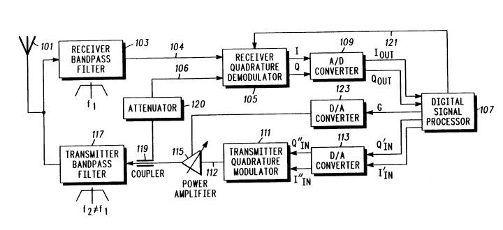
FIG. 1 shows a block diagram of a transceiver including
a transmitter, a receiver and a signal processor portion. A
typical received signal, a received time slot in a TDM signal,
is coupled through an antenna 101 into a receiver bandpass
20 filter 103. The filtered response 104 is quadrature
demodulated in the receiver quadrature demodulator 105. The
demodulated signal is composed of In-phase (I) and
Quadrature-phase (Q) components. The I and Q quadrature
components are coupled to a digital signal processor 107
25 through a sampling Analog-to-Digital (A/D) converter 109.
A typical transmitted signal, a transmit time slot in a
TDM signal, originates in the digital signal processor 107 and
i8 further coupled to a transmitter quadrature modulator 111
as I"IN and Q"IN signal components through a Digital-to-
30 Analog (D/A) converter 113. The transmitter quadraturemodulator 111 combines the I"IN and Q"IN signal components
into a transmitter excitation signal 112. The excitation signal
112 is amplified with power amplifier 115 and further coupled
to the antenna 101 through a transmitter bandpass filter 117.
2~9~76
The receiver b~n-lr~s filter 103 and the transmitter bandpass
filter 117 each pass a different frequency range to isolate the
receiver and transmitter portions of the transmitter.
In the preferred embodiment of the present invention, a
5 coupler 119 couples a portion of the output signal of the power
amplifier 115 to the receiver quadrature demodulator 105
through the attenuator 120. The purpose of the attenuator 120
is to reduce the signal level out of the coupler to levels within
the dynamic range of the receiver in a controlled m~nner. A
-- 1 0 rece~ver control signal 121 from the digital signal processor
107 configures the receiver quadrature demodulator 105 to
receive a signal either from the ~ntenn~ 101 or the output of
the transmit amplifier 115. ~imil~r receiver circuitry in the
receiver quadrature demodulator 105 is used to demodulate
1 5 sign~ls from both sources.
FIG. 2 shows a portion of the receiver quadrature
demodulator which selects between two candidate sign~l~ 104
and 106 depen-ling on the state of the receiver control signal
121. The receiver control signal 121 activates switch 405 to
20 select whether the received signal is coupled from the antenna
101 or from the transmitter amplifier 115. When the switch
contact 410 is coupled to terminal 406, mixer 407 and local
oscillator 409 convert the transmit signal 106 from power
amplifier 115 to the normal IF frequency processed by mixers
25 401 and 403. Likewise, when switch contact 410 is coupled to
terminal 408, mixer 417 and local oscillator 415 convert a
received carrier signal 104 from the antenna 101 to the normal
IF frequency processed by miyers 401 and 403. Separate local
oscillators 409 and 415 are used because of different transmit
30 and receive frequencies. Local oscillator 411 and 90 phase
shifter 413 provide conventional receiver demodulating
functions. The output of mixers 401 and 403, I and Q
component sign~l~, respectively, are coupled to A/D converter
109.
2069'17~
The advantage of using simil~r receiver circuitry
allows additional hardware, otherwise necessary to receive the
transmit amplifier output signal 106 to be çlimin~ted. The
state of the receiver control signal 121 is determined using
5 timing information recovered from the normal receive signal.
The receiver control signal 121 determines which signal
will be received based upon the operating position of the
transmit and receive time slots in a TDM signal for the
transceiver. During the transceiver's receive time slot, the
10 receive control signal 121 instructs the receiver quadrature
demodulator 105 to receive a carrier signal 104 from the
~qntenn~ 101. During the transceiver's transmit time slot, the
receive control signal 121 instructs the receiver quadrature
demodulator 105 to receive the transmit signal from the power
1 5 amplifier 115.
During the transceiver's transmit time slot, the receiver
quadrature demodulator 105 receives the power ~mplifier's
output signal 106 from the coupler 119 coupled through the
attenuator 120. The receiver quadrature demodulator 105
20 demodulates the output signal into its quadrature components
which are further coupled to the digital signal processor 107
through an A/D converter 109 resulting in component signals
Iout and Qout.
Component sign~ls, IoUt and Qout.1 are processed in the
2~ DSP 107 to adjust the input signal of the power amplifier 115.
The adjusted input signals, I'IN and Q'IN, are coupled from
the DSP 107 to the D/A converter 113 as I"IN and Q"IN, and
further to the transmitter quadrature modulator 111. The
transmitter quadrature modulator 111 modulates the
30 quadrature signal components, I"IN and Q"IN, into a
transmitter excitation signal which is further ~mplified by the
power ~mplifier 115. The input signal level to the power
~mplifier 115 is adjusted with a correction value which results
in an output signal that is linear with the original input signal
2~9~
before adjustment. The output of the power amplifier 115 is
coupled through a transmitter bandpass filter 117 into the
antenna 101. The gain control signal, H, determined by the
DSP 107, is coupled through the D/A converter 123 to the power
5 amplifier 115.
As described above, the gain nonlinearity of power
amplifier 115 is compensated for by adjusting the input signal
level presented to the power amplifier 115 by modulator 111
based on what the energy of the input signal is, to compensate
10 for the gain nonlineArity of the power amplifier. The
nonlinearity of the power Amrlifier may be described as a
variation of gain with the input signal level. The correction
value is determined by sampling the output signal of power
Amplifier 115. The input and sampled signAl~ in DSP 107
15 update the correction value used for each input signal level.
Factors that cause operation in the amplifiers nonlinear
region include large-signal gain variations, saturation and
cutoff effects, temperature, input signal level variations, and
the disturbance of internal bias points by reflected energy at
20 the transmit amplifier output due to the voltage st~n(ling wave
ratio (VSWR) of the antenna. It is also desirable to chose to
operate the amplifier in the non-linear region because the
amplifier is more efficient in the non-linear region.
Compen~Ation for non-linearity permits a net increase
25 in the efficiency of the power amplifier 115. Advantages of an
efficient power Amplifier 115 may be applied to both fixed and
mobile transceivers using a power amplifier. Specific
advantages in a mobile or portable transceiver include: longer
talk time, smaller battery size, cooler operation and increased
30 reliability.
Now referring to FIG. 3 there is shown a block diagram
of a signal processor which may employ the present invention.
The following text describes the general process of how the
~0~9ll76
1 1
amplifier's output signal, IOUT and QOUT, is processed in the
DSP 107 to determine an adjusted input signal, I'IN and Q IN-
The receiver selector 215 determines the state of thereceiver control signal 121. The receiver selector 215 makes its
5 decision based on the time state of the TDMA received
channel.
The data source 207 provides the Iin and Qin quadrature
component ~ign~l~ for transmitting. The TDM time clock 206
synchronizes the data source's transmitting activities and the
10 selection of modes for the dual-mode receiver quadrature
demodulator 105 of FIG. 1. The quadrature data is coupled to
the linearizer 211 as Iin and Qin through a low pass filter 213.
The linearizer 211 has four outputs: Pin and K(Pin) coupled to
the inverse transfer function determiner 205 and I'in and Q'in
15 coupled to the D/A Converter 113.
The linearizer 211 determines Pin from input siFn~ls,
IIN and QIN, looks up a K(PIN), a correction value, in the look-
up table and multiplies Iin and Qin each by the K(P~N) which
results in a gain-adjusted transmitter excitation input signal,
20 I'in and Q'in, coupled to modulator 111. The adjusted input
signal, I'in and Q'in7 provides an amplified signal at the output
of the transmit ?~mplifier 115 which is linear with the input
signal Iin and Qin-
The lookup table consists of correction factors which
25 apply to each input signal level, to result in a net linear gainrelationship between input signal level and output signal level.
This table is updated during each transmit time slot of the
power ~mplifier 115 as the transceiver operates, so that
changes in ,qmplifier transfer function characteristics are
30 corrected for soon after they occur.
For each discrete sample pair of Iin and Qin, input
signal power is calculated by the signal processor, after the
low-pass filtering process is performed using the following
equation:
2 ~
Pin = (Iin2 + Qin2)
PIN determines from the look-up table the level of Iin and Qin
5 should be adjusted to maintain a linear relationship between
input and output of the power amplifier 115. The look-up table
has as many entries as is necessary to correct for variations in
power amplifier gain accurately. In the preferred
embodiment, a table of 100 entries corrects for Amplifier gain
10 variations over a 50dB range of signal power, in 0.5dB steps.
Since there is a single entry in the table for each input signal
level, the look-up table is subst~ntiAlly smaller than the
complex-valued correction look-up table cited previously.
The look-up table is periodically updated by the inverse
15 transfer function determiner 205 to reflect possible changes in
the power ~mplifier's distortion characteristics. For instance,
the linearity of the amplifier is dependent on the load
impe~Ance presented to it by the AntennA of the transceiver.
This load impedance, in turn, is dependent on the proximity of
20 metal objects to the antenna, thus as the transceiver moves it
is desirable to update the look-up table.
In the preferred embodiment of the present invention,
the inverse transfer function determinator 205 uses a coarse
gain factor, H, the recovered transmit si~nAl~ Iout and Qout,
25 Pin and K(Pjn)~ the correction value for PIN SignAl~ from the
linearizer in order to determine the inverse transfer function's
optimum gain correction value, K'(Pjn)~ This, in turn, is used
to correct the current K(Pjn) value.
The look-up table is periodically updated with new
30 correction factor entries as the nonlinearity of the g_in of the
power Amplifier changes. The receiver portion of the dual-
mode receiver demodulates an attenuated sample of the power
amplifier output signAl. Receiver quadrature output signAls,
Iout and Qout,are used to measure the transmitter gain for
2~6~
given gain-corrected transmit amplifier input signal level of
(K(Pin)2)(Pin) from
The output signal level: Pout = (Iout2 + QOut2)~ and
given a known attenuation D in the attenuator and coupler.
The transmit amplifier gain, G', for gain-corrected transmit
amplifier input level, (K(Pin)2)(Pin) can be derived from:
G'(Pin) = Pout/((D)(pin)(K(pin)2)
In general, G'(Pin) is not a constant except for truly linear
amplifiers. An ideal linear gain, G, is desired. Consider
quantizing the e~pected range of Pin into a discrete set of
15 values. Based on values of G'(Pin) obtained as above, for each of
the observed values of Pin during the course of transmitter
operation there e~ists a optimum correction factor K'(Pin),
K'(Pin) = (G/G'(Pin))0 5
where G is a known desired net gain, and G'(Pin) is a
measured value.
During normal operation, the table of correction factors
is applied to Iin and Qin to generate corrected I in and Q'in
25 values for the gain error (and hence distortion) occurring at
that particular Pin level. The table is also iteratively updated to
reflect changes in distortion, according to the following update
equation:
K"(Pin) = K(pin) - (alpha)K (PIN)
Where K'(Pin) is the updated gain adjustment value for a
particular observed Pin.
206~34~6
1 4
The constant alpha is a small error-correction factor.
Thus each entry in the table is adjusted by a portion of the
observed actual correction factor, when the input power Pin for
that entry occurs in the modulation signal, to steer the entries
5 in the correction table toward the actual correction factors, as
the actual correction factors drift over time.
If it is found that K(Pin) differs greatly from 1, to the
point that the adjusted I'in and Q'in values would fall outside
the useful range of the modulation D/A converters, the overall
10 transmitter gain may be adjusted via a separate control signal
applied to an adjustable gain stage prior to the transmitter
amplifier. In this case, the proper correction factor becomes:
(H)(K(Pin)) = (G/(G (Pin))0 5
1 5
Where H is the gain of the adjustable gain stage at the
adjustable gain level for which K(Pin) is calculated; thus as
errors in measured G'(Pin) are corrected on a per-sample
basis by K(Pin), dependent on Pin, an overall course gain
20 correction is applied via the constant H, which reduces the
requirements on the modulation D/A converters for handling
a wide range of output levels.
As an alternate embodiment of the present invention,
the look-up table may be substituted with a power series
25 calculation. For this alternate embodiment, the output signal
from the inverse transfer function determinator, K"(Pin), is a
correction to the coefficients of a gain adjustment power series
equation.
It is possible to derive the gain correction values for
30 modulation samples using an appro~imation to the transmit
amplifier transfer function and a derived inverse transfer
function. Instead of deriving a table-based set of correction
factors, a pair of equation matrices are solved to return the
coefficients of a correction power series, an inverse transfer
2~S9~76
function power series, which is applied to the gain of Iin and
Qin~ to generate I in and Q'in. For 2~ and y vectors of input and
output signal energy, each entry in 2~ being one of the set of
values Pin corresponding to a value Pout measured at the
5 output of the transmit amplifier, a corresponding entry in y,
we have the system of equations:
al(~D + a3(~3) + as(~5) + ... + an(~n) = Y
10 Where the ak coefficients, k > 1, are the distortion terms of the
transmit ~mplifier transfer function expressed as a power
series. Knowing measured values of the vector y and
corresponding values of 2~. we can solve n equations in n
unknowns to obtain the values an
15 to the desired order of non-linearity n. An inverse transfer
function can then be derived by solving the system of
equations:
bl(f(~D) + b3(f~D)3 + bs(f(~))5 + ... + bn(f~))n = (G)(2~)
where f(2~) is the power series producing y, above. This
set of equations is solved for the coefficients bk with a set of
input values of ~ and measured resultants y, to produce a
power series which, when applied to the input energy,
25 produces a norm~li7ed output energy. To correct nomin~lly for
up to 5th order non-linearity, this requires solving two sets of
equations, each 3 equations in 3 unknowns.
As with the table method, the coefficients of the inverse
transfer function can be corrected as the transmit ~mplifier's
30 transfer function changes with operating conditions by
calculating new coefficients periodically, and using a portion
of the new coefflcients to steer the current coefflcient estimates
toward their optimum values.
16 206~476
In the preferred embodiment, the value Pin i8 calculated
for each new set of Iin,Qin values generated at the output of the
modulation low-pass filters. This Pin value is then applied to
the estimated inverse transfer function to produce a value P in,
5 which is the desired input power level required to produce the
desired output power level when processed through the non-
linear transmitter amplifier. A correction factor is calculated:
K(Pin)=(Pin/Pin)05
this then multiplies, in the same mPnner as the lookup-table
entry in the preferred embodiment, Iin and Qin, in order to
produce the desired P'in power which will generate the desired
linear-gained instantaneous output power, resulting in a net
15 linear gain for the particular Iin and Qin modulation signal
pair.
FIG.4is a graph showing three curves relating the
input energy level to the output energy level of the power
amplifier. The input energy level of the power ~mplifier is
2 0 denoted by EIN on the abscissa. The output energy level of the
power Pmplifier is denoted by EOUT on the ordinate.
The three curves on the graph represent a transfer
function 305, an inverse trPn~fer function 307, and an ideal
linear transfer function 309 of the power ~mplifier 115.
25 Generally, the transfer function of the power Pmplifier 115 will
follow the transfer function curve 305. The slope of the curve is
linear throughout most of its operating region. The graph
shows nonlinePrity be~inning at a coordinate point 304. Above
this transition point the power amplifier 115 no longer has a
30 linear transfer function characteristic. The slope of the
transfer function curve 305 decreases whereby an incremental
change in the level of the input signal, does not produce a
correspond ng incremental change in the level of the output
signal.
.,~,~
.-
20~476
The preferred embodiment of the present inventiondescribes a process to determine the transfer function curve
305 and the inverse transfer function curve 307 for the power
amplifier 115. Using signal processing, an inverse transfer
5 function representing the difference between curves 307 and
309 (~n be determined from the transfer function 305. By
applying the inverse transfer function as a table of correction
values to the transfer function curve 305, a related net linear
transfer function curve 309 is determined.
1 0 In the preferred embodiment, the amplifier 115 operates
within non-linear region to improve efficiency. The effect of
the inverse transfer function determin~tor 205 is to determine
the coordinate point 311 on transfer function curve 305 and
determine a second coordinate point 313 on the inverse
1 5 transfer function curve 307. Each point is an equal distance
from a third coordinate point 315 on the linear function 309.
Other sets of equal distance points, not labeled, are also shown
to indicate the relationship between the three curves.
An adjustment signal representing a measure of the
20 ratio of point 313 on the image curve 307 to point 315 on the
linear curve is multiplied by the input sign~ls Iin and Qin f
the transmitter quadrature modulator 111 in order to adjust
the transmit ~mplifier input signal resulting in a linear
output signal at the coordinate point 315 on the linear transfer
25 function curve 309. Thus, the transfer function and its inverse
are determined to effectively linearize the transfer function of
the power ~mplifier 115 over its nonline~r operating range.
Thus, by adjusting the input signal to the power
amplifier 115, an effective linear transfer function is
30 determined, based on a measured signal collected at the
output of the transmitter ~mplifier by a dual-mode receiver.