Note: Descriptions are shown in the official language in which they were submitted.
2~6~3g
1-
ACTI~ FILTER CIRCUIT
Background of the Invention
~e pre~ent ~nvelltion relates generally to filter
cir~itry, and, more particularly, to an active filter disposed
upon an integrated circuit which has a variable, or otherwise
~electable, band~ndth for pa~sing signal por~on~ of desirsd
Prequenc~s of a SigIlal applied there~o.
'I'he de~ign of and u~ of filter circuitry for pas~ing
desirqd iignal component portions of a signal, and for filtering
und~sired, 3igl~al component portion~ of the signal, is well
known. For e~ample, filter circuitry which perfiorm3
bandpas~, band reject, low pa3s, high pass, an~ combina~ions
thereof, are all well~known. 5uch filter circuitry, or
combinatio~ thereof, form portion3 of electrical c~rcuits ~o
pass ~or reject) ~ignal componen~ portions of ~ignals applied to
the filter :ireuitry.
Historic~lly, Blter circuitry was ~Sr3t comprised of
passiYe fileer components formed of coils (i.e. inductors),
tra~formers, and capaQtors. Such component~ were
adYantageou~ly utilized ~o form filter cir uitry having
e2tr~mely accurate filter characteristic~. Howe~er, such
cla~sical filt~r component~ are both expensiYe ar d bulky.
Electr~cal circuits, of which the filter circuit~ o~entimes
comprise a portion, include electrical circui~s forming
portions of communication systems. A communication
system is comprised, at ~he rninimum, of a trans~tter and a
'
2~9639
receiver interconnected by a transmission channel upon
which an information si~al may be transmitted.
Transmitters, receivers, and other communication ~ystem
circuitry is becoming in reasingly miniaturized, and
5 competition between manufacturer3 thereof is becoming
increasingly price-competitive. Because filter circuitry forms
a portion of such device~, filter circuitry is similarly becoming
increasingly miniaturized, and more price-competitive.
Therefore, filt~r circuitry has been developed which i3
10 both of a smaller SiZB, and i9 less costly to produce, than filter
circuitry comprised of classical element~. For e2arnple, some
active ~lter circuitry components may be advantageausly
embodiet in an integrated cir~uit which i3 both of small size,
and of low cost to produce.
As mentioned hereinabove, filter circuitry frequently
forms a portion of electr~cal circuit~ utilized by a
communication 3ystem. One particular type of
communication system, a radio communication system, i~
compriset of a transmitter and a receiver interconnectet by a
20 radio-frequency channel. To transmit an information signal
upon the radio-frequency channel, the information signal is
impressed upon a radio-frequency, electromagnetic wave by a
proce~ referred to a~ modulation. The radio-frequency
elec~romagnetic wavQ is of a characteristic frequency ~ithin a
25 ra~ge of fr8qu~ncie3 which defines the radio-frequency
ehannel.
l'he ~dio-frequency, electromagnetic wave, refsrred to
a8 a c~Tier wave, once modulated by the information signal,
is referred to a~ a motulated, information ~ignal. The
30 motulatedS information signal may be tran~mitted through
free ~pace to transmit thereby the information between the
transmitter and the rPceiver. Modulation techniques have
been developed to create the modulated, information signal by
combining the carr~er wave and an in~ormation signal. Such
'~ :
2 ~ 3 9
3 -
modulation techniques include. for example, amplitude
modulation (~M), frequency modulation (F.~), phase
modulation (P.~), and complex modulation (C~I).
A receiver, forming a portion of the radio
S communication system, r~ceives the modulated, infor~nation
signal, once generated by the transmitter and t~ansmitted
thereby over the radio~frequency channel. The receiver
includes circ~t2y to detect, or to recreate otherwise, the
information signal modulated upon the radio firequency,
electromagnetic wave. Such circuitry is referred to as
demodulation circuitry, and the process of detecting, or
otherwise recreating, th2 in~ormation signal i9 referred to ag
demo/dulation. The receiver typically further includes
circuit~ to convert the ~requency of the radio-frequency,
modulated, information signal to permit proper operation o~
the demodulation circuitry. Usually, such circu~try convert~
the modulated, information signal downward in frequency,
and is referred to a~ down COnVerSiGn circuitry.
A receiver additionally contains tu~ing circlait~y
including filter c~rcl~try forming passbands for passing
signal component portion~ of signals received by the receiver.
The raceiver do~n conversion circuitry, and the receiver
demodulatio~ circuitry may additionally contain filter
circuitry to prevent passage of undesired signa~3.
The broad range of ~requencies at which modulated.
in~ormat;iol~ signals may be transm~ttet is re~erred to as the
eleetromag~letic frequency spectmm. Regulatory authorities
have divided the electromagnetic êrequency spe~trum into
frequency bar~d~, and the frequency bands into transrni5sion
chann01s upon which the modulated, informatiorl ~ignal~ may
be tran~mitt~d. Such regulation minim~2es intefference
beS~reen simultaneously transmitted signal3.
For example, portlons of a 100 MHz band of the
electrQma~Fnetic frequency spectrum which extends between
- - : ' ' ., ~". ,, ::
2 ~ 3 ~9
800 and 900 MHz are allocated, in the United States, for
radiotelephone communication. Radiotelephone3 utilized in a
cellular, communication system transmit and receive radio
fr~quency, modulated information signals at fr~quencies
5 ~nthin 3uch frequency band.
Numerous base stations form the infrastructure of a
cellular. communication system. A ~ase station contains
circuit2y to receive and to transmit modulated, information
9ignals. By po8itioning ba3e 3tation9 at spaced-apart locations
throughout a geographical area, reception and transmission ~ ~ .
of modulated, irlformation signals to and from radiotelephones
located in the vicinity of individual one9 of the base ~tations to
permit two-way communication therebetween. Appropriate
positioning of the ba~e ~tation~ at ths spaced-apaIt locations
15 throughout the geographical area cau~es at least one of the
base ~tations to be ~ithin the transmi~ion/reeeption range of
a radiotelephone located at any position ~nthin the
geographical area. A portion of the geographical area
pro~mat8 to a base station is re!!e~Ted to a3 a "cell", and each ~ .
20 base station defi~le~ thereby a cell. Numerous cells defined by
each of the numerou~ base stations fo~s the cellular
communicstio~ sy~tem throughout the geographical area.
~ lthough numerou~ modulat~d, informatioll signals
may be tran~mitted 3imultaneously upon difYerent
25 transmi9~io~ channels (i.e., a~ different transmission
f~equencies), each modulated, informa~ion si~al occupies a
~Dite po~oa~ of the allocated frequency band, i.e., a
ion channel, and only a limited number of
transmi~sion channels in the allocated frequency band are
30 available to pe~it simultaneous transmission thereupon.
Increased usage of cellular, communication systems
ha~ resulted, in many instances, in full utilization of every
available transmi~sion channel oî the allocated frequency
band. As a re~ult, various suggestions have been proposed to
-
- .. : ., '
,
.
2~639
utilize more efficiently the frequency band allocated for
radiotelephone communication. .~Iore efficient utilization of
the frequency band would incr~ase the information
transmission capacity of a radiotelephone communication
5 sy~tem. Variou~ ~uggestions have similarly been proposed to
use more efficiently other frequency bands of the
electromagnetic frequency spectrum allocated for other uses.
A modulated, in~ormation si~nal is spread-out over a
band of ~requencie8 centered at, or close to, the frequeney of the
10 ~arrier wave. This span of frequencies over which the
modulated, information sign81 i9 spread is referred to as the
bandwidth of the signal. The banduidths of the radio-
frequency transmission chanrlels into which the frequency
band allocated for cellular communications is divided, must be
t 5 of 3i2es such that modulated, information ~ignals transmitted
simultaneously over adjacent transmission channels do not
overlap. However, the transmissiQn channels must be wide
enough to permit transmission of the entire modulated,
information sigr~als thereupon, but additionally, permit a
20 certain amount of frequency drif~ of the signals as the signal9
are transmitted upon the transmission channels. That i3, the
channel spacing defining the transmission channel
bandw~dths mu3t be great enough to persnit frequency drift of
~imultan~ou~ly-transmitted, modulated, in~ormation 9ignal!i
25 on a~ adja&ent channels in which one, or more, of the ~ignals
e~hibit ~r~quency drif~.
Tran~rnit~er circuitry of transmitters which generat~ :
and tran~mit the modulated, informa~ion signal~ upon the
tran~mis~iorl cbannels, generate signals which are somewhat
30 smaller than the channel bandwidth. The channel bandwidth
i9 wide enough to permit simultaneous transmission of
si~al~ on adjacent channels even when th0re is significant
frequency drif~c (a~ a percentage of the bandwidth of the
.
'. .
. : .
6 3 0~
trans~itted 3ignal) of the signals tran~mitted upon the
adjacent channel~.
As commercially~viable methods and apparatus for
reducing signal bandwidth of transmitted signals, and for
S m~n~m~zing frequency drift of the transmitted signal~ are
developed and implemented, the bandwidth~ of the
tran~ ion chalmels uporl which the signals are
tran~m~tted may be reduced. A reduction in the bandwidths of
the tran9mission channel~ would permit a great8r number of
1 û transm~sion channel~ to be defined for a frequency band,
~uch a~ the frequency band allocated for cellular
commur~ication~. For irl~tanc~, in the Urlited State3, a
portion, e~tending between 824 MHz and 849 MHz, is allocated
for the transmis~ion of modulated information ~ignals from a
15 radiotslephone to a base ~tation. A second portion, e~tending
between 86g MHz and 894 MH2 of the frequ~ncy band is
allocsted for the trarasmis~ion of modulated i~formation
~ignals from a base station to radiotelephone. Each of the
transmission chaImelq of the first and second portions of the
20 allocated freque~cy band i~ of a bandwidth of 30 KHz. By
reducing the size of the bandwidth~ of the transmission
channel~ firom 30 KH2 to 15 ~z would re~ult in a doubling of
capacity of a c~llular communication system within a
particular ~eographical ar~a. The conventional-3ized
25 transm~ssion ch~nnel is referred to as a wideband bandwidth
channel, and the tran~mission channel of reduced si~e i5
re~rred`to as a narrowband bandwidth.
~ 3uch a reduction in transmission channel bandw~dth~
howe~er, require~ alteratioll of the infrastructure (that i9, the
30 base stations) as well as the radio~elephone~ utilized in such a
system. Becau~a such an alteration of the infrastructure
n~ces ita~e3 ~ignificant capital expenditure3, only those
cellular communication systems which are presently, or are
anticipated to be, fully utilized, need to be altered to permit
:~ :
2~639
greater numbers of the transmission channels to be defined
therein. However, to perrnit operation of a radiotelephone in
both existing cellular communication systems and cellular
communications systems in which the capacity thereof is
S increased, the radiotelephones must contain circuitry to
pe~nit operation thereof in either an existing system or a
system of expanded capacity.
To permit operation of a single radiotelephone in both
eristing systems and systems of e~panded capacity requires
circuitry to permit reception of either signals of normal
bandwidths, or signals of reduced bandwidths. Most simply,
iuch a radiotelephone could be designed to have separate filter
c~rcuitry, each havislg passbands of dif~erent bandwidths (i.e.,
~oth the w~deband bandwidth and the narrowband
bandwidth). One or the other of the ~Iter circuitry would be
operative depending UpOIl, for e~ample, in which sys~em the
radiotslephone is located, or depending ~pon the band~vidth of
the signal transmittetl thereto. However, because of the
increased miniaturization of radiotelephones, the utilization of
additionsl filter circuitry would limit further miniaturization
of the radiotelephone. Therefore, a sin~le filter circuit which
i~ operable to pass either a motulated information signal of
normal balld~idth, or, alternately, a modulated info2mation
signal of reduced baI~twidth would be beneficial.
What i8 needed, therefore, is a radiotelephone
construction having filter circuitry, of minimal size, which
~rmit~ rec~ption of modulated, information signal~ of
band~r~dehs oorresponding to the bandwidths of Sigllal9
generat~d in a conventional, cellular communication system,
or a cellular, communica~ion system of increased capac~ty.
.
2 ~ 3 9
8-
S~nmary of the Invention
It is, accordingly, an object of the present invention to
provide filter circuitry having a variable passband for
perm~tting reception of a 3ignal of either a first bandwidth, or
a second bandw~dth.
It i~ a further object of the present invention to provide
filter circ utry hav~ng a variable passband for a radiotelephone
to permit thereby reception of both a wideband signal and a
narrowbant signal.
It is a yet further object of the present invention to
pro~ide active filter circuitry, disposed UpOIl an integrated
c~rcuit, having a variable bandwidth.
In accordance with the present invention, ther~fore, an
actiYe filter circ-i~t hav~ng a variable passband operative to
pass signal portions of a received signal is disclosed. The filter
circuit is disposed upon an integrated circuit aad compr~ses a
filter defining at least one passbaIld of a desired ban~w~dth
hav~ng arl upper cut-o~ ~equency and a lower cut-off `~
freq1~ency for passing signal portions of a received signal
having ~requ~ncie~ within the desired bandw~dth. The desired
bandwidth of the pa~band of the filter is selected by the
application of a control signal to the filter.
Brief De~cription of the DraMngs
l~e pres~nt invention vill be better understood when
read in light ot' the accompanying drawings in which:
FIGs.lA and lB are graphicalrepresentation~ofa
typical, modu~ated,info~nation signal graphed as a fimction
offrequency; :
FIG. 2 is a graphical representation of several adjacent
transmis~ion channel~ of the frequency band allocated for
' . ' .
,
2 ~ 9
cellular communications formed of a portion of the
electromagnetic frequency spectrum;
FIG. 3 is a graphical representstion, similar to that of
FIG. 2, but illustrating the simultaneous transmission of
modulated, informa~on ~ignals upon adjacent channels of the
a cellular, commuI~ication system wherein signals of
bandw dths representstiYe of a conventional, cellular
~omm~Lnication ~y~tem are shown at the lef~-hand side portion
of the figure, arld ~ignal~ representative of signals generated
in a cellular communication system of expanded capacity are
~hown in the r~ght-hand side portion of the figure;
FIG. 4 is a graphical repre~entation of a modulated,
information signal transmitted upon a transmission channel
in which a noi~e, or other undesired, signal i~ located, in
frequeIlcy, pro~imate thereto;
FIG. 5 is a circl~t schema~dc of an LC filter circll~t
which fiorms a pa~sband of a bandwidth and cu~o~ freq~encies
of value~ deter~ned by the value~ of the component elements
thereof;
FIG. 6 i~ a circuit schematic of a filter c~rcuit, similar to
that of FIG. 5, but having transeonductance elements and
capacitors compri~ing the component elements thereof; and
FIG. 7 is a block diagram of a radiotelephone of the
present ~n~ention in which the filter of FIG. 6 form~ a portion
thereo
Description of a Preferred Embodiment
Turni3~g first to the graphical representation of FIG.
lA, a modulated, information signal, referred to generally by
referenc2 numeral 10, is plotted as a function of frequency~
The smplitude of signal 10, scaled in terms of volts on ordina~e
a.lds 14, is graphed a3 a fiLnction of frequency, scaled in terms
of hertz, on absc~a axi3 18. Signal 10 i9 representative of the
.
. .
'
3 9
10 -
signal formed by modulating an information signal by one of
the pre~riously-mentioned modulation techniques, ~or e~ample,
I, FM, PM, or C~ techn~que.
The energy of the modulated, information si~al, such
5 8~ signal 10, formed by one of these modulation techniques is
typically centered about a c~nter frequency, fc of a particular
frequency. The center frequency, in most instaIlces, is the
ca~er freqliency. The re~ultant, modulated, information
signal, here ~ignal 10, is 3ymmetrical about the cen~er
10 frequency, fc~ Vertically-extending line 22, shown in hatch,
which i~ defined by the center frequency,fc, indicatei ~uch
symmetry of signal 10 thereabout.
Ihe bandwidth of signal 10 i~ indicated by the length of
arrow 26. A receiver circuit which receive~ a modulated,
15 information signal, such as signal 10, includes filter circuitry
having passbands at least as wide as the bandwidth of the
modulated, information signal to recreate, in undistorted
foTm, the info~mation signal~ Because of frequency drift
associsted with the transmission of radio-frequency sigIlals!
20 the bandwidth of the filter circuitry of the receiver is typically
greater than the bandwidth of the transmitted signal.
The graphical representation of FIG. lB i8 3imilar to
that of FIG. lA in which modulated information signal 10 is
plotted a~ a fi nc~on of frequency. The amplitude of signal 10, . .
25 scaled in te~3 of volts on ordinate axis 14, is graphed as a
fimstio~ of ~requency, ~caled in terms of hertz, on abscissa
18.`` The graph sf FIG. lB further illustrates sig~al 30
characterized by frequencies close to the frequencie~
encompa~s~d by the bandw~dth of signal 10. Signal 30 i~
30 representative of, for e~mple, a spurious noise signal or a
modulated, information signal transmitted UpOIl a
transmussion channel adja~ ent to the transmission chann~l
upon which sigalal 10 is transmitted, but which has drif~ed in
frequency. For purposes of illustration, the amplitude of
h 3 ~
gig~lal 30 i9 greater than the amplitude of signal 10. Signal 30
may alternately be of ~n amplitude equal to or less than the
plitude of the ~ignal lO.
~deally, a receiver constructed to receive signal lO
S contains filt~r circuitry having passbands of bandwidths to
receive signal 10 in tLndisto~ted form, but to prevent passage of
unwanted ~i~als, ~uch as signal 30. However, as mentioned
h~reinabove, the pa~sbands of the filter circuitry of a recei~rer
ar~ typically greater than the bandwidth of the modulated,
10 information signal (here, signal 10) to ensure that the entire
~ignal i3 passed in undistoree~ form even when significant
frequency drif~ of the transm~tted signal occurs. Such an
enlarged bandwidth i~ indicated in FIG. lB by arrow 34. Filter
circuitry having a passband corresponding to the bandwidth
15 indicated by arrow 34 per~nits passage of signal 10 in
undi~to~d form, but, additionally, permits pa~sage of
unw~nted ~ignals such as, and as indicated in the Figure, a
portion of sig~lal 30. In in~tances, and as illustrated in FIG.
lB, in which the unwanted signal i9 of a significant amplitud~
20 relative to the amplitude of signal 10 there, signal 30 is of an
amplitude greater than the ampliSude of signal 10), the
resu1tant signal recreated by a receiver would contain
significant i~ renee, caused by the unwanted signal or
portion ther~of. I here~re, it would be de~irable ~o be able tQ
25 decresse the bandwidth of the passbands of the filter circuitry,
a~ desired, to prevent passage of unwanted signals located in
frequency`clos~ to a modulated,inforrnation si~al.
Turning no~v to the graphical representation of FIG. 2,
a portion ofa frequency band representative of a portion ofthe
30 frequency band allocated for cellular communications is
illustrated. 5imilar to the graph of FIG. 1, the ordinate a~s,
here a~ 38, i~ scaled in tenns of volts and abscissa axis, here
a~s 42, i9 ~caled in terms of hertz. As mentioned pr~viously,
portion3 ofthe frequency band allocated for cellular
.
~0~9~3~
-
- 12 -
communication are divided into transmission channels
whereupon a single signal i3 transmitted at a time upon any,
or all, of the transmission channels to prevent overlapping of
simultaneously transmitted signals. Signals ~ransmitted
upon adjacent, or other, transmission channels may, of
course, be sirnultaneously transmitted.
FIG. 2 illustrates fiYe of such transmission channels,
here referred to by reference n~ erals 46, 50, 54, 58, and 62.
In FIG. 2, each transmi5sion channel 46-62 is of a 30 KHz
bandw~dth. Such a bandwidth colTesponds to the bandw~dths
defined for transmission channels of existing, United States,
cellular commtmication systems. Transsnission channels
defined upon other cellular. comr~unications system3 may b~
similarly illustrated with appropr~ate substitution of other
transmission channel bandwidths. For instance, the
transmission channels defined in e~isting, Japanes~, cellular
communicatior~ ~ystems of are 25 KHz bandwidths. Other
channelized communications systems may similarly be
described with appropriate substitu~on of frequency
demarcation~.
The vertical lines spaced at the 30 KHz intervals
represent boundarie~ between adjacent ones of the
tran3mission channels 46-62. ~odulated, information
signals, such as signal 10 of FIGs. lA and lB may be
txan~mitted ~multaneously upon any or all of the
t~a~m~ssioll channels 46-62 as long as the bandwidths of the
signals trangmitted upon individual ones of the channels 46-62
ar8 not of sizes to oYerlap with signals transm~tted upon
adjac~nt ones of the transmission channels.
Control of the bandwidths of the signals transmitted is
required, not only to prevent overlapping of simultaneously
transmitted signals, but, additionally, because the passbands
of the receiver filter circuitry are, in most instances, of
magnitude~ corresponding to the bandwidths of the
. .
. ~ - . .
- ~ :
~ .~ .... . ~ . . .
2~63~
- 13-
transmission channels. If a signal transmitt~d upon one of
the transmission channels is of too large of a bandw~dth, or
the frequency drift of the signal causes the transmitted signal
to be partially, or wholly, beyond the passband of the filter
5 c~rcuitry, the signal demodulated by the receiver will be
distorted.
Signals 66 and 70 are positioned within channels 46 and
50, respectively, of FIG. 2. Signals 66 and 7Q are similar in
shape and bandw~dth to slgnal 10 of FIGs. lA~lB, and are
10 representative of modulated, information sigr.als generated
and transmitted by a conventional transmiSter. Further
illustrated in FIG. ~ is signal 74 positioned within the
boundaries of transmis~ion channel 5~. Signal 74 is
representati~e of a modulated, in~rmation signal ~enerated
l 5 a~ld transmitted by a transmitter of a ne~er construetion and
is of a bandw~dth of one-half OE the size of the bandw~dth of
signal 68 and 70. While methods and apparatus ~or
transn~itting small bandwidths signals have been previously
available, technical improvements have permitted the
2û construction of co2r~nercially-viable transrrLitters capable of
transmitting signals of such reduced bandw~d$hs.
Hi~torically, the channel spacing determining channel
bandw~dth~ of th~ tran~mission channel~, such as
transmissioR chann~l~ 46-B~ of FIG. 2, of the ~requency band
2~ allocat~d for cellular communications was defined to ensure
that transmi~ter~ utilizing commercially-viable technology
could transmit channels of bandwidths less than the
bsndwidths of the transmission channels. As illustrated,
however, the ~andwidth requirements of signal~ generated
30 and transmitted by newer, and now commercially-viable,
transmitters penn~t~ significant portions of each channel of
the frequency band alloca~ed for cellular communications to be
unused. However, by re defining the bandwidths of the
channels of the allocated ~equency band to reduce thereby the
: . :
.
.
` 2~9639
.
bandwidths of some, or all, of the channels. greater nurnbers
of channels may be defined over the allocated frequency band.
Greater nu~bers of signals could then be transmitted
simultaneously upon the increased number of transmission
5 charmels, thereby increasing the transn~ssion capacity of the
cellular. commun~cation system.
FIG. 3 is graphical representation. similar to that of
FIG. ~, defining an ~s sy~tem wherein ordinate axis 38 is
9~1ed in terms of volt~, and abscissa axi3 42 is scaled in terms
10 of hertz. Similar to FIG. 2, the transmission channels of FIG.
3 have boundaries represented by vertically e~tending lines.
I~e le~-hand side portion of the Figure illustrate~
transm~ssion channel~ 7~ and 82 of bandwidths similar to the
bandw~dehs of transmission channels 46-62 of FIG. 2. Signals
1 S 86 and gQ of bandwidths similar to the bandwidth3 of signals 66
aIld 70 of FIG. 2 ar~ again representative of signals g~nerQted
and tran~mitted by transmitter~ of conventional con~truction.
The right-hand side portion of FIG. 3, however, illu~trates
four transm~ssion channel~ 94, 98, 102, and 106, of bandwidths
20 one-half the size of the bandwidths of transmission char~nels
78 and sa. Transm~tted upon channels 94-106 are signals 110,
114, 118, and ~22. Signals 110-122 are of barldwidths similar to
the bandwidth8 of signal 74 of FIG~ 2, and, theret!ore, are of
bandwidths of o~e-half of the size of the bandwidth9 of signal3
~5 86 and 90. Companson of the le~-hand sida portion and the
right^hand sid~ portion of the graph of FIG. 3 illustrat&s that
h/tice ~he number of the signals may be simultaneously
tran~mitted in a system in which the transmission channels,
a~d th~ ~ignals transmitted thereupon, are one-half the size of
30 the trans~i3sion channels of a conventional system.
Becau8e the ~umber channels of the right-hand side
portion of FIG. 3 i9 a multiple of the channels ot` the leflc-hand
3id~ portion thereof, the channel spacing of the right hand
side portion of the Figure is compatible with the channel
, - . . .
~9~3~
spacing of the lef~hand side portion thereof. A cellular,
Gommun~cation system may therefore form a system in which
transmission cham~els of more than one bandwidth may be
defined. It is noted that a system in which the channels of
5 another multiple (such as, for example, a multiple of three
would sim~larly define a system compatible with existing
systems.
In order to properly recreate the in~orrnation signal
portion of a transm~tted ~ignal, radiotelephone receiver
10 circuitry should contain filter circuitry for passing only the
desired signal. Becauset as prev~ously mentioned, the receiver
corltains filter circuitry ha~ving passband~ correspondirlg to
the bandwidths of the transmission channel~ upon which a
signal i~ transmitted, a receiver of a radiotelephone operable
15 ~n either a conventional system or a system of increased
capac~ty would require filter circuitry having passband~
corresponding to the bandwitths of transmissiorl channel~ of
a conventional ~ystem, and of bandwidths corresponding to a
system of increased capacity. Because of the ever increasing
20 miniaturization of electronic good~, such as radiotelephones,
it would be desirable to have a radiotelephone constmction
having a ~ gle filter circuit capable of forming a passband of
a ~rariable band~ridth.
FIG. 4 illu~trates a single transmission channel I2~
25 upon which moslulated, information signal 130 is transmitted.
Positioned pronmate to signal 130, in ~requency, is noi e
signal 1~. A portion of signal 134 is within the bandw~d$h of
smis~ion channel 126. A radiotelephone construction
having fil~r circuitry capable of forming a variable passband
30 i~ additionally advantageou~ for the reason that the passband
of the filter may be redueed to prevent passage of those portions
of noise signal 134 ha~ing frequencie~ within the range oî
frequencies defined by the passband of transmission channel
126. That is, the passband of the filter c~rcuitry may be
- .
. ~
.. ~ . . .
: . ~
.
-` 2069~3~
. 16
-
adjusted, or fine-tuned, to prevent passage of the noise
portions, when present.
Tulning now to cir~uit diagram of FIG. 5, an LC filter
circuit, referred to generally by reference numeral 150, is
shown. Filter circuit 150 i~ formed by capac~tor~ 154, 158, 162,
and 166 positioned in a parallel connection wherein first sides
of capacitors 164 and 158 are connected through inductor 170,
first sides of capacitors 158 and 162 are connected through
inductor 174, and first sides of capacitor~ 162 and 166 are
~nterconnected by inductor 178. Capacitor 182 is additionally
positioned in parallel with inductor 170 between first sides of
capac~tors 154 and 158. Second sides of capacitor~ 154 166 are
suitably connected there together, and preferably, and as
illu~trated, are coupled to a ground connectioll. Filter circu~t
150 further illustrates curTent source 186 connected in a
parallel conn~ction with resistor 190, and additionally in
parallel with the parallel connection of cap citors 154 -166.
Current ~ource 186 may be representative of a wideband,
received signal which i9 received by a radiotelephone. Filter
circuit 150 of FIG. 5 further includes resistor 194 colLnected in
parallel ~nth capacitor 166 across which an output voltage
may be measuret. Filter circuit 150 forms a passband of a
frequency band~id~h determined by the values of capacitors
154-166 and 182, and inductors 170-178. The passband of the
filter circuit 150 may, of course, be altered by altenng ehe
Yalues of the component elements thereof.
Turi~ing now to circuit schematic of FIG. 6, a circuit
equivalent to ~lter CiFCUlt 150, here referred to generally by
reference numeral 250, is shown. Equ~valent filter circuit 250
i~ compr~sed by circuit component element~ Çormed of
capadtors and transconductance element
Transconductance elements of the equivalent filter c rcuit 250
are substituted for the inductors 170-178 of the filter c~rcuit 150
of FIG. 5 for rea30ns to be discussed more ~ully hereinbelow.
.' ,~
.
2 ~ 9
. 1,
Similar to capacitors 154-166 and 182 of t~lter circuit 150 of FIG.
5, equivalent filter circuit 250 includes capacitors 254, 258. 262,
and 266 which are connected in a parallel connection.
Connecting first sides of capacitors 254 and 258 is capacitor
282. Second side.~ of capacitors ~54-266 are suitably connected
theretogether, and preferably, as illustrated, are connected to
ground potential.
Outputs of l;ransronductance elements 286 and 290 are
coupled to node 294 (which further has first sides of capacitors
254 and 282 connected thereat). A negative input of
transconduc~ance element 286 and a positive input of
transconductance element 298 is further coupled at node 294.
A negative input to transconductance element 2~8 is coupled to
node 302 as i~ a positive input to transconductance element
306, and the output of transconductance element 310
(additionally, second side of capacitor 282 and first s~te of
cap~citor 258 are coupled thereat). Similarly, a negative input
to transconductance element 306 is coupled to node 314 as i5 a
positi-~e input of transconductance element 318, and the output
of transconductance element 322 (additionally, first side of
capacitor 262 is coupled to node 314). A nega~ive input to
transconduct~nce element 318 is coupled at node 326 as are the
output and input of transconductance element 330.
Po~itiYe irlputc to transconductance elements 286 and
~5 290 are couplet directly to ground; a negative input to
transconductance element 290 is coupled to ground through ::
capacitor 334 a~ i~ the positive input to transconductance
element 310. The negative input to transconductance element
310 i~ coupled to ground ~hrough capacitor 342 as is the
positive input to transconductance element 322. The negative
input to transconductance element 322 is coupled to ground
through capac-tor 338 as is the positive input to
transconductance el~ment 330. Outputs of transconductance
~:
`:
,
2~9~39
- 18-
elements 298, 306 and 318 are coupled to ground through
capacitors 334, 338, and 342.
The use of transconductance elements as component
elements of equi~alent filter circu~t 250 is advantageous for the
5 reason that transconductance element3 may be easily disposed
upon an integrated circuit. Additionally, the character~stics of
transconductance elements may be quickly altered ~ alser
thereby the characteristics, namely, the passband, o~ the
eq~valent filter circ~ut 250 formed thereby. Filter circuit 250 of
10 FIG. 6 further illustrates current source 350 which, simitar to
current source 188 of FIG. 6 may correspond to a w~deband,
rec~ive signal received by a radiotelephone receiver.
The integrated circuit upon which filter circuit 250 i~
disposed, aceording to th~ preferred embodiment of the present
15 invention, further has disposed thereupon ~n o~cillator, which
is also compr~sed of transconductance element~. Tracking
betwecn elements, and particularly the transconductance
elements, upon a single integrated circuit is a well kno~n
phenomena. Such tracking between the tran~conductance
20 elements form~ng a portion of filter circuit 250 and
transconductanc~ elements forming a portion an oscillator
may be advantageously utilized to maintain the reiative
frequencies of the passband of the filter formed of filter circuit
250 and the 03cilla~ng ~requency of the oscillator disposed
25 upon th~ integrsted circuit with the same external reference,
3uch a~ an esternsl crystal oscillator. Thereby, the cut-o~
firequen~s of the passband formed of filter circuit 2S0 may be
precisely controlled.
Appropriate control ~ignals may be applied to the
30 transconductar~ce elements of the filter circuit 250 to vary the
passband of the filter circuit to pass signals within bandwidths
of transmission channels, such as transmission channels 78
and 82 of a conven~ional, cellular communication system
illustrated in FIG. 3, or, alternately, to be of a passband of
2 ~ 3 9
- 19-
bandw~dths corresponding to the transmission channels of a
cellular, commumcatlon system o~ increased capacity, such
as transmis~ion channels 94-106 of FIG. 3. Variation (i.e.,
fine tuning) of the actual bandwidth9 of the passbands of the
filter circuit 250 may additionally be adjusted responsive to the
presence of noise, such a~ noi9e signal 134 of FIG. 4,
pro:cimate in frequellcy, to a desired signal, such as signal 130
of FIG. 4. The e~stcnce of such noise may be indicated, for
e~ample, by determining, and monitor~n~ a ratio of si~al
1 Q plus noise-to-noise and distortion (a signal commonly referred
to as a SINA~ sig~al), or a conventiorlal, RSSI signal, the
gerleratioll of either of which are well known per se in the art.
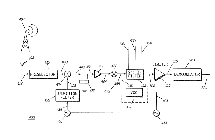
Turni~g now to the block diagram of FI&. 7, a
radiotelephone, r~fe~red to generally by reference numeral
400, con3tructed according to the teachings of the present
un~ention i~ illustrated. The actual circu~tay embodying the
fi~nctional blocl~s of the diagram may be disposed upon one or
more circuit board~ and housed within a conventional
radiotelephone hou~ing.
Radiotelephone 400 utilizes the active filter circlait of
FIG. 6 compL~ed of ~ransconductance elements and
capa~tors to form a vanable filter of a pas band of a desired
bandw~dth thQreby. The use of such filter ciret~trg perm~t~
operation of radiotelephone 400 to receive signals tran~mitted
in a co~re~tional, cellular communication system, or,
alternately, ill a c~llular, communication system of increased
capRcity. A transmitted signal transmitt~d by a ba~e 3tation,
hera represellted by transmitt~r 404, i5 reeeived by
radiotelephone asltenna 408.
Antenna 408 supplies the received si~al on line 412 to
preselector/filter 41~. Preselector/filter 416 iq pre~erably a very
wideba~ld filter ha~ing a passband to pass all of the
frequencies within a band of interest. Filter 416 gen0rate~ a
filtered signal on line 420 which is supplied to mi~er 424.
3 ~
-20-
Mi~:er 424 additionally receives an oscillating signal on line
428 from injection filter ~32, which is, in turn, supplied an
oscillating, input signal on line 436 by oscillator 440. Oscillator
~0 is locked in frequency with the oscillating frequency of
5 oscillator 444 which, for example, may be compr~sed of a
crystal oscillator. Oscillator 440 and filter 432 may together
form a portion of a conventional phase locked loop. Mi~er 424
generate3 a down converted ~ignal (commonly reÇerred to as a
first interm~diate, frequency, i.e., IF, signal) on line 448
10 which is supplied to filter 452. Filter 452 is, preferably, and a~
illustrated, a monolithic crystal wideband filter (commonly
referred to as the first intermediate ~requency, i.e., IF, filter).
Filter 452 generates a filtered signal on line 45O which is
~upplied to amplifier 460. Amplifier 460 amplifie the signal
15 supplied thereto on line 4~6 and generates an arnplified 9ig~
on line 464. Llne 464 i9 coupled to an input of mixer ~68 which
also receives an input on line 472 from oseillator 476. As
mentioned hereinabove, osc~llator 476 i~ preferably disposed
upon an integrat~d circuit, and sueh integrated circuit i~
20 indicated in the figure by block 480, shown in hatch. Ihe
os~illating fi~e~uency of oscillator 476 is locl~ed to the oscillating
frequency of oscillator 444 by the connection therebetweell by
line 484. ~i~er 468 generates a mi~ed signal 011 line 488 which
is supplied to filter 492. Filter 42, refie~Ted to as the seco~d
25 i~termediat~ Prequency filter, is similar to the equivalerlt filter
circuit of FIG. 6, ant is disposed upon the same integrated
circu~t as oscillator ~76 (as indicated by block 480, shown in
hatch). Control signal inputs to filter 492 are indicated by lines
496, 500, snd 504, which correspond ~o an external input signal
30 for selecting the bandwidth of filter d~92 to pa~s a signal
transmitted by a conventional, cellular, communication
system or one of increased capacity, a SINAD signal, and an
RSSI signal, respectively. As mentioned hereinabove, the
SINAD and RSSI signals supplied on lis~es 500 and 504 fine
.~ . ,
~` 2 ~ 3 ~
tune the bandwidth of the passband of filter 492. Filter 492
generates a filtered signal on line 508 which is supplied to
limiter 512. L~miter 51~ generates a ~oltage-limited signal on
line 516 which i~ supplied to the demodulator 520.
5 Demodulator 520 is comprised of conventional demodulation
circuitry for demodulating the signal supplied thereto and
prov~ding an output on li~e 524.
The Aigr~al supplied of line 496 may, for example, cause
the filter to be of a first bandw~dth when the signal is beneath a
10 certain value, and be of a second bandw~dth when the signal is
beyond the certairl value. Additionally, filter passbands of
three (or even more) di~erent bandw~dths responsive to valu~
of the signal suppliet to filter 492 on line 496 may be formed.
for e~ample, when the signal on line 496 is beneath a first
15 level, a narrowband filter may be selected, when the signal on
line 4g~ is beyond 8 second le~rel, a wadeband filter may be
selected, and wh~n the ~ignal on line 496 i9 between the first
and the ~econd level3, a midband filter having a passband of a
bandwidth le~s th~n the wideband filter, but greater than the
20 bandw~dth of the narrowband filter, may be selected.
Becau~s the bandwidth of the passband of filter 492 i~
variable, a single filter circuit disposed upon a single
integrated circuit may be utilized to permit reception of a
9igllal generated by a eransmitter of a conventional, f~ellular
25 communication system, or of a cellular, communication
3yst~m of irlcrea~ed capacity. Fine tuning of ~he bandw~dth of
~e pa~sband to r~nimize signal degradation and other
problem3 as~ociated w~th noise is facilita~ed by the application
of the SINAD and R3SI signals on lines 500 and 504. Still
30 fiurther, becau~e of the tracking of the tran~conductance
element~ of both o~cillator 476 and filter 492 dispo~ed upon the
single integrated circui~ 480, precision of ehe actual cut-o~
frequen~ies which define the bandwidth of the passband of
filter 492 may be controlled.
9~39
22 -
While the present invention has been described in
connectiorl with the prefe~Ted embodiments of various figures,
it i~ to be under~tood that similar embodiments may be used
and modifications and addition~ may be made to the descr~bed
5 elnbodi~ents for performing the same functions of the present
invention w~thout deviating therefiorn. Therefore, the present
inYention should not be limited to any single embodiment, but
rather cons~rued iR breadth and ~cope in accordance with the
recitation of the appended claim~.
What i~ claimed i~:
.