Language selection

Search

Patent 2069658 Summary

Third-party information liability

Some of the information on this Web page has been provided by external sources. The Government of Canada is not responsible for the accuracy, reliability or currency of the information supplied by external sources. Users wishing to rely upon this information should consult directly with the source of the information. Content provided by external sources is not subject to official languages, privacy and accessibility requirements.

Claims and Abstract availability

Any discrepancies in the text and image of the Claims and Abstract are due to differing posting times. Text of the Claims and Abstract are posted:

  • At the time the application is open to public inspection;
  • At the time of issue of the patent (grant).
(12) Patent: (11) CA 2069658
(54) English Title: ACTIVE INTELLIGENT TERMINATION
(54) French Title: TERMINAISON INTELLIGENTE ACTIVE
Status: Deemed expired
Bibliographic Data
(51) International Patent Classification (IPC):
  • H03H 11/28 (2006.01)
  • G06F 13/00 (2006.01)
  • G11C 5/06 (2006.01)
  • G11C 7/10 (2006.01)
  • H03K 5/1252 (2006.01)
(72) Inventors :
  • OKURA, DAVID KAZUO (Canada)
(73) Owners :
  • NORTEL NETWORKS LIMITED (Canada)
(71) Applicants :
  • OKURA, DAVID KAZUO (Canada)
(74) Agent:
(74) Associate agent:
(45) Issued: 1998-09-15
(22) Filed Date: 1992-05-27
(41) Open to Public Inspection: 1993-01-26
Examination requested: 1994-04-13
Availability of licence: N/A
(25) Language of filing: English

Patent Cooperation Treaty (PCT): No

(30) Application Priority Data:
Application No. Country/Territory Date
735,730 United States of America 1991-07-25

Abstracts

English Abstract


An active intelligent termination circuit is designed to function
as a self-switching clamp adapted to attenuate unwanted signals on a
data bus. A field effect transistor is switched on or off in a
conducting mode or non-conducting mode respectively in accordance with
the data transmitted on the data bus. Any low level unwanted signals
which may appear on the bus when data having a voltage level
corresponding to a logic zero is present will be attenuated by the field
effect transistor which is coupled to both the data bus and to a ground
plane. The field effect transistor switches to the non-conducting mode
when data corresponding to a logic level one is transmitted on the bus.


French Abstract

L'invention est un circuit de terminaison intelligent actif conçu pour fonctionner comme dispositif de calage à autocommutation adapté pour affaiblir les parasites sur un bus de données. Un transistor à effet de champ est commuté à l'état conducteur ou à l'état non conducteur selon les données transmises sur le bus. Les parasites de faible niveau qui peuvent se manifester sur le bus quand des données ayant un niveau de tension correspondant au niveau logique zéro sont présentes seront affaiblis par le transistor à effet de champ, lequel est couplé au bus de données et à un tapis de sol. Le transistor à effet de champ passe à l'état non conducteur quand les données correspondant au niveau logique un sont transmises sur le bus.

Claims

Note: Claims are shown in the official language in which they were submitted.


WHAT IS CLAIMED IS:

1. A circuit for attenuating unwanted signals on a
transmission line adapted to carry data signals comprising:
an inverter gate coupled to the transmission line for
providing inverted data signals corresponding to the signals appearing on
the transmission line;
a flip-flop responsive to the inverted data signals and to a
local clock signal for providing output signals;
circuit means connected to the flip-flop for providing inverted
output signals thereof;
an AND gate responsive to the inverted data signals and to
the inverted output signals from the flip-flop to provide ANDED signals;
and
a controllable transmission gate connected between the
transmission line and terminal connected to a reference voltage, the
controllable gate being responsive to the ANDED signals for providing a
conducting path to the terminal from the transmission line in a first mode
and for preventing conduction between the transmission line and the
terminal in a second mode.

2. The circuit as defined in claim 1 wherein the controllable
gate is a field effect transistor.

3. A circuit for attenuating unwanted signals on a
transmission line adapted to carry data signals, comprising:
a controllable transmission gate operable in a first mode for
conducting unwanted current from the transmission gate to a voltage
reference terminal in response to unwanted signals on the transmission
line and operable in a second mode for preventing the conduction of
current from the transmission line to the terminal, the gate having a first
terminal connected to the transmission line, a second terminal connected
to the voltage reference terminal and a control terminal, and a control
circuit means for releasing the transmission gate from conducting in the
first mode in response to a clock signal and to the data signals on the
transmission line, said control circuit means being coupled to the


transmission line via an inverter gate and having a control circuit output
connected to the control terminal of the controllable transmission gate.

4. A circuit as defined in claim 3 wherein the control circuit
means comprises:
a flip-flop responsive to the inverted data signals and to a
local clock signal for providing output signals;
inverting circuit means connected to the flip-flop for
providing inverted output signals thereof; and
an AND gate responsive to the inverted data signals and to
the inverted output signals from the flip-flop to provide control signals to
the controllable transmission gate.

Description

Note: Descriptions are shown in the official language in which they were submitted.


2QS9658
'.~.


Active Intelligent Termination


Field of the Invention
The invention relates generally to a circuit and method for
attenuating unwanted signals on a transmission line.


Background of the Invention
During the transmission of a signal on a transmission line, signal
energy is transferred most efficiently when no reflected wave is
present. Thus to obtain a transmission of energy with a maximum
efficiency, it ;s necessary to provide means for matching any actual
load impedance to the characteristic impedance of the transmission line.
However, only under exceptional cases will the load impedance be a
15 resistance that is exactly equal to the characteristic impedance of the
line. In many instances a load can be matched to the characteristic
impedance of a line by coupling to the load a network of reactances that
tunes out the network and load reactance and simultaneously transforms
to a value equal to the characteristic impedance of the line; in other
20 instances where the actual load or number of loads on a line may be
variable or not precisely known, active termination circuits may be
used.
United States Patent number 4,748,426 issued May 31, 1988 in the
name of Alexander Stewart discloses an active termination circuit having
25 a resistor combination permanently connected to a bus that couples a
plurality of peripheral devices to one another. Other ends of the
resistors are coupled to a positive voltage supply line and to a logic
ground plane, respectively. Stewart teaches active impedance matching
by on/off control of switches which open or close paths to the
30 resistors.

5 8


Computer systems and telecommunication ystems often have a
plurality of source and destination nodes connected to and sharing a
common data transmission facility such as a bus. These nodes may simply
be receivers and transceivers located on circuit packs electrically
5 coupled to the bus. Such systems are often designed to be flexible,
permitting variable configurations; the capability is therefore provided
for an operator to add or remove circuit packs according to the
particular requirements. In a system having loads which vary from time
to time according to the configuration of circuit packs connected to the
10 bus, it may be difficult to provide adequate terminations to eliminate
unwanted signal reflections. In addition, in systems where any
particular node may transmit data to one of many possible receiver nodes
and the distance between the respective nodes is variable, it is
difficult to predict and provide the form of termination that will be
15 required.
In an attempt to overcome some of the aforementioned limitations
it is an object of the invention to provide a circuit for attenuating
unwanted signals.
The invention provides an active self~switching clamp which is
20 adapted to attenuate unwanted signals having a voltage level which
varies from a logic zero level by a small increment.


Summary of the Invention
In accordance with the invention there is provided a circuit for
25 attenuating unwanted signals on a transmission line adapted to carry
data signals comprising: a controllable transmission gate operable in a
first mode for conducting unwanted current from the transmission gate to
a voltage reference terminal in response to unwanted signals on the
transmission line and operable in a second mcde for preventing the
conduction of current from the transmission line to the terminal, the
gate having a first terminal connected to the transmission line a
second terminal connected to the voltage reference terminal and a

5 8


control terminal, and a control circuit means for releasing the transmission
gate from conducting in the first mode in response to a clock signal and
to the data signals on the transmission line, said control circuit means
being coupled to the transmission line via an inverter gate and having
its output connected to the control terminal of the controllable
transmission gate.


Description of the Drawings
The invention will be described in conjunction with the drawings
0 in which:
Figure 1 is a schematic diagram of a bus including a plurality of
receivers and transmitters coupled to termination circuits;
Figure 2 is circuit diagram of an embodiment of the termination
circuit of figure 1, having self-switching capability; and
Figure 3 is a circuit diagram of an alternative embodiment of the
invention for use with a tri-stateable bus.
In figure 1 a bus 10 is connected to a plurality of transceivers
13. Each transceiver 13 is coupled to a termination circuit 11. It
will be understood that an arbitration scheme may be implemented to
20 prevent bus contention and that a transceiver 13 is capable of
broadcasting over the bus 10 to more than 1 transceiver 13.
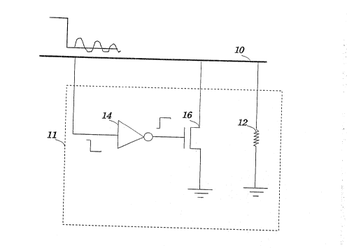
Figure 2 shows the bus 10 connected to the termination circuit 11
which includes a resistor 12, an inverter 14, and an n-channel field
effect transistor (NFET) 16. The resistor 12 is an off-the-shelf
25 termination resistor having predetermined resistance. Both the NFET 16
and the resistor 12 are coupled to a ground plane having a voltage
corresponding to a logic zero value or zero volts. As a form of


~..

20S9G58
illustration, a portion of a digital signal having a hi to lo transition
is shown having superimposed thereon an unwanted alternating signal. It
is desirable to eliminate unwanted signals, caused by reflection, noise,
or the like which may not totally be absorbed by conventional
s termination means such as the termination resistor 12. If the magnitude
of any reflected signals becomes too great, transmitted data may become
corrupted. For example, if a zero bit is being transmitted, and the
unwanted signal reaches a voltage level near the threshold level
associated with switching from one logic state to another, the
transmitted zero bit may be perceived as a one-bit.
In the preferred embodiment shown in figure 3, a flip-flop 20 is
coupled to an inverter 14 and to an AND gate 22 having inverted input
terminals. An NFET 16 is similarly configured as in figure 2 having the
source and drain connected to the bus 10 and to a ground plane
15 respectively. The circuit shown in figure 3 is suitable for use on a
tristatable bus. The flip-flop 20 allows the NFET 16 to switch on and
conduct thereby eliminating most of any unwanted signals, and releases
the clamp after the data on the bus has been latched. A detailed
description of the operation of the circuit will follow.
With reference to figure 2, the termination circuit 11 provides a
means of self-switching and clamping unwanted spurious reflected signals
which otherwise may be perceived as one-bits instead of transmitted
zero-bits. The NFET 16 performs the function of clamping when switched
on, in a conducting mode. In the instance that a one-bit followed by a
25 zero-bit is transmitted as is illustrated by the waveform in figure 2,
the zero-bit received at the input terminal of the inverter 14 results
in a one-bit at its output terminal. This one-bit corresponding to a
digital hi voltage level switches on the gate of the NFET 16 thereby
providing a path to ground. In the instance that a one-bit is presented
30 to the input terminal of the inverter 14, a resulting zero-bit
corresponding to approximately zero volts switches off the NFET 16
preventing it from conducting and isolating the bus 10 from the ground
plane. It should be obvious to a person skilled in the art that the
transceivers 13 must be adequately powered to provide enough current to

2069658
allow the NFET 16 to switch off. More specifically, the transceivers
must supply enough current to overpower a switched on conducting NFET to
allow the NFET to switch off.
In the preferred embodiment shown in figure 3, as data on the bus
5 10 changes from a one to a zero the NFET 16 switches on and conducts
thereby reducing unwanted signals by providing a path to ground. One
clock cycle later the zero-bit of data is inverted and is clocked
through the flip-flop and the clamp is released, the NFET switching off
and not conducting. If the data on the bus 10 changes from a zero to a
1, the clamp remains released and the NFET does not conduct. In the
event that the bus becomes tristated, a pull-up resistor 24 provides a
voltage corresponding to a logic hi, and the NFET remains switched off
and in the non-conducting mode of operation. The flip-flop 20 and the
AND gate 22 essentially provide a means of releasing the clamp one clock
15 cycle after the data has been available on the bus 10.
Numerous modifications and variations may be considered without
departing from the scope of the invention.

Representative Drawing
A single figure which represents the drawing illustrating the invention.
Administrative Status

For a clearer understanding of the status of the application/patent presented on this page, the site Disclaimer , as well as the definitions for Patent , Administrative Status , Maintenance Fee  and Payment History  should be consulted.

Administrative Status

Title Date
Forecasted Issue Date 1998-09-15
(22) Filed 1992-05-27
(41) Open to Public Inspection 1993-01-26
Examination Requested 1994-04-13
(45) Issued 1998-09-15
Deemed Expired 2005-05-27

Abandonment History

Abandonment Date Reason Reinstatement Date
1997-05-27 FAILURE TO PAY APPLICATION MAINTENANCE FEE 1997-09-10

Payment History

Fee Type Anniversary Year Due Date Amount Paid Paid Date
Application Fee $0.00 1992-05-27
Registration of a document - section 124 $0.00 1992-12-18
Maintenance Fee - Application - New Act 2 1994-05-27 $100.00 1994-04-13
Maintenance Fee - Application - New Act 3 1995-05-29 $100.00 1995-05-23
Maintenance Fee - Application - New Act 4 1996-05-27 $100.00 1996-05-15
Reinstatement: Failure to Pay Application Maintenance Fees $200.00 1997-09-10
Maintenance Fee - Application - New Act 5 1997-05-27 $150.00 1997-09-10
Final Fee $300.00 1998-05-06
Maintenance Fee - Application - New Act 6 1998-05-27 $150.00 1998-05-06
Maintenance Fee - Patent - New Act 7 1999-05-27 $150.00 1999-04-01
Registration of a document - section 124 $0.00 2000-02-02
Maintenance Fee - Patent - New Act 8 2000-05-29 $150.00 2000-05-18
Maintenance Fee - Patent - New Act 9 2001-05-28 $150.00 2001-05-18
Maintenance Fee - Patent - New Act 10 2002-05-27 $200.00 2002-05-24
Registration of a document - section 124 $0.00 2002-10-30
Maintenance Fee - Patent - New Act 11 2003-05-27 $200.00 2003-04-15
Owners on Record

Note: Records showing the ownership history in alphabetical order.

Current Owners on Record
NORTEL NETWORKS LIMITED
Past Owners on Record
BELL-NORTHERN RESEARCH LTD.
NORTEL NETWORKS CORPORATION
NORTHERN TELECOM LIMITED
OKURA, DAVID KAZUO
Past Owners that do not appear in the "Owners on Record" listing will appear in other documentation within the application.
Documents

To view selected files, please enter reCAPTCHA code :


To view images, click a link in the Document Description column. To download the documents, select one or more checkboxes in the first column and then click the "Download Selected in PDF format (Zip Archive)" or the "Download Selected as Single PDF" button.

List of published and non-published patent-specific documents on the CPD .

If you have any difficulty accessing content, you can call the Client Service Centre at 1-866-997-1936 or send them an e-mail at CIPO Client Service Centre.


Document
Description 
Date
(yyyy-mm-dd) 
Number of pages   Size of Image (KB) 
Cover Page 1994-03-27 1 16
Abstract 1994-03-27 1 23
Claims 1994-03-27 2 57
Drawings 1994-03-27 3 45
Representative Drawing 1998-08-19 1 5
Description 1994-03-27 5 201
Claims 1997-04-30 2 65
Description 1997-04-30 5 189
Cover Page 1998-08-19 1 43
Representative Drawing 1998-10-15 1 6
Assignment 2000-08-31 2 43
Assignment 2000-01-06 43 4,789
Correspondence 1998-04-16 1 103
Correspondence 1998-05-06 1 39
Correspondence 2000-02-08 1 22
Fees 1999-04-01 1 33
Fees 1997-09-10 1 45
Fees 2001-05-18 1 40
Fees 2002-05-24 1 32
Fees 1998-05-06 1 37
PCT Correspondence 1997-09-10 2 54
Office Letter 1994-05-10 1 72
Prosecution Correspondence 1997-04-09 2 78
Examiner Requisition 1997-02-21 2 63
Prosecution Correspondence 1994-05-18 1 33
Prosecution Correspondence 1994-04-13 1 44
Office Letter 1998-02-05 1 18
Office Letter 1998-02-05 1 20
Fees 1996-05-15 1 36
Fees 1995-05-23 1 37
Fees 1994-04-13 1 37