Note: Descriptions are shown in the official language in which they were submitted.
CFO 8482 ~069708
- 1 -
1 PROBE-DRIVING MECHANISM, PRODUCTION THEREOF, AND
APPARATUS AND PIEZOELECTRIC ACTUATOR EMPLOYING THE
SAME
BACKGROUND OF THE INVENTION
Field of the Invention
The present invention relates to a
piezoelectric actuator, a probe-driving mechanism,
methods of production thereof, and an apparatus
employing the same such as a tunnel current-detecting
device and an information-processing device.
Related Background Art
In recent years, application of STM technique
is investigated in a variety of technical fields
including observation and evaluation of semiconductors
and high-molecular materials in atomic or molecular
order, fine working, and recording apparatus.
In particular, recording apparatuses are
required to have large capacity in calculation
information and image information of a computor, and
so forth, and development of STM technique therefor is
more and more strongly demanded. As the result of
progress in semiconductor processing technique,
microprocessors have come to be miniaturized and
computing ability has been improved. Consequently,
recording apparatuses are desired to be further
- 2 - 2069708
1 miniaturized. To satisfy such requirements, a
recording-reproduction apparatus is disclosed which
employs a transducer having a tunnel-current-
generating probe provided on a driving means capable
of fine adjustment of the gap between the probe and a
recording medium. This apparatus records information
by applying voltage with the transducer to change the
work function on the surface of the recording medium,
or reads out information by detecting the change of a
tunnel current caused by the change of the work
function, at the minimum recording area of lO nm
square (Japanese Patent Application Laid-Open No.
63-161552).
Generally, the probes need to be increased in
number in order to accelerate transfer and recording
of data. In the transfer or recording of data in the
aforementioned apparatus, the probes run along the
lines of recorded data by adjusting the space between
the probe and a recording medium. Since the breadth
Of the lines of the recorded data is extremely small,
stable recording-reproduction cannot readily be
achieved owing to the drift caused by the temperature
variation of the apparatus, run-out of the probes from
the data lines caused by external vibration, and other
influences. Accordingly, the respective probes are
required to move independently in high speed in a
2069708
- 3 -
l direction perpendicular to the face of the recording
medium.
To satisfy such requirement, W089/07256, for
example, discloses a cantilever constituted of
lamination of piezoelectric material layers 5, 7 and
electrode layers 4, 6, 8 as shown in Fig. 6. The
cantilever is prepared by forming an insulating layer
11 composed of silicon oxide film, patterning it, and
etching anisotropically a substrate 1 to have a
bimorph arm 10.
In the above example of the prior art,
however, the thickness of the insulating layer 11
needs to be made thin to suppress side-etching of the
Si substrate 1 in the etching of the bimorph arm 10
and the insulating layer 11. Thereby, nonnegligible
capacitance is induced between the lower electrode 4
and the Si substrate 1, forming an equivalent circuit
by connection with another electrode through the
substrate as shown in Fig. 7.
Usually, the driving frequency of a cantilever
is limited by the resonance frequency determined by
the dimension and the layer constitution of the
cantilever. In the example of the above prior art,
the driving frequency is limited also by the increase
Of the time constant caused by the capacitance induced
by the piezoelectric substance layers 5,7 and the
2069708
1 aforementioned parasitic capacitance. Consequently,
the adjustment of the spacing between a medium and the
probe becomes impossible and malfunction arises in
writing and reading. In a multi-probe construction,
difference in lengths of wiring to the driving
electrodes for respective probes causes large
variation of the parasitic capacitance, which causes
variation of the driving characteristics of the
cantilever.
If the insulating layer under the electrode is
made thick to reduce the parasitic capacity for the
purpose of avoiding the above problems, Si is
isotropically etched, when the insulating layer 11 is
etched, in the side direction in a dimension of ten
times larger or more than the thickness of the
insulating layer as shown in Fig. 6, which lowers the
controllability of the cantilever.
SUMMARY OF THE INVENTION
An object of the present invention is to
provide a novel piezoelectric actuator and a probe-
driving mechanism, in which the parasitic capacitance
induced between the cantilever and the support is
reduced to improve the responsibility of the
cantilever and unnecessary etching is prevented, and
also to provide a method of production thereof.
2069708
- 5 -
1 Another object of the present invention is to
provide an information processing apparatus comprising
a tunnel current-detecting device employing the above
probe-driving mechanism improved in accuracy and
responsibility, and means for recording, reproduction,
and erasing.
According to a first aspect of the present
invention, there is provided a probe-driving mechanism
comprising a bimorph cantilever having a thin
piezoelectric substance film and electrodes holding
the film therebetween and being supported by a support
at one end, and having a probe for information input
and output at the other end: the probe-driving
mechanism having a first insulating layer between the
support and the cantilever, and a second insulating
layer at the other side of the support, and the first
insulating layer having a sufficient thickness to
reduce parasitic capacitance induced between the
electrode of the cantilever and the support.
According to a second aspect of the present
invention, there is provided a process for producing a
probe-driving mechanism, comprising steps of providing
a first insulating layer on a support, providing a
second insulating layer on the other side of the
support, laminating an electrode layer and a thin
piezoelectric substance layer successively on the
2069708
-- 6 --
1 first insulating layer, forming a probe, and removing
the support to form a cantilever.
According to a third aspect of the present
invention, there is provided a multi-probe-driving
mechanism, having two or more of the above probe-
driving mechanism arranged two-dimensionally.
According to a fourth aspect of the present
invention, there is provided a tunnel current-
detecting apparatus, comprising the above prove-
driving mechanism counterposed to an electricconductor, a driving means for driving the probe-
driving mechanism, a control means for controlling the
driving means, a voltage-applying means for applying
voltage between the electric conductor and the probe,
a detecting means for detecting a tunnel current
between the electric conductor and the probe, and an
outputting means for outputting information on the
surface of the electric conductor according to
detected tunnel current.
According to a fifth aspect of the present
invention, there is provided an information-processing
apparatus, comprising the above probe-driving
mechanism counterposed to a recording medium, a
driving means for driving the probe-driving mechanism,
a control means for controlling the driving means, and
a voltage applying means for applying pulse voltage
_ 7 _ ~ 2 ~ 6 g 7 0 8
l between the recording medium and the probe for
information recording.
According to a sixth aspect of the present
invention, there is provided an information-processing
apparatus, comprising the above probe-driving
mechanism counterposed to a recording medium, a
driving means for driving the probe-driving mechanism,
a control means for controlling the driving means, and
a voltage applying means for applying bias voltage
between the recording medium and the probe for
information reproduction.
According to a seventh aspect of the present
invention, there is provided an information-processing
apparatus, comprising the above probe-driving
mechanism counterposed to a recording medium, a
driving means for driving the probe-driving mechanism,
a control means for controlling the driving means, and
voltage-applying means for applying pulse voltage for
information recording and applying bias voltage
between the recording medium and the probe for
information reproduction.
In the above-mentioned three aspects of the
present invention with regard to information-
processing apparatus, a surface of the recording
medium may be non-conductive.
According to an eighth aspect of the present
2069708
- 8 -
1 invention, there is provided a piezoelectric actuator,
comprising a bimorph cantilever having a thin
piezoelectric substance film and electrodes holding
the film therebetween and being supported at an end by
a support; a first insulating layer between the
cantilever and the support; and a second insulating
film on the other side of the support, and the first
insulating layer having a sufficient thickness to
reduce parasitic capacitance induced between the
electrode of the cantilever and the support.
According to an ninth aspect of the present
invention, there is provided a process for producing a
piezoelectric actuator, comprising steps of providing
a first insulating layer on a support, providing a
second insulating layer further thereon, laminating an
electrode layer and a thin piezoelectric substance
layer successively on one of the insulating layers,
and removing the support to form a cantilever.
BRIEF DESCRIPTION OF THE DRAWINGS
Fig. 1 is a sectional view of a probe-driving
mechanism of the present invention.
Figs. 2A to 2C illustrate a process for
producing a probe-driving mechanism.
25Fig. 3 illustrates another process for
producing a probe-driving mechanism of the present
2069708
g
l invention.
Fig. 4 is a rough sketch of a multi-probe.
Fig. 5 illustrates outline of an information-
processing apparatus of the present invention.
Fig. 6 illustrates roughly an example of prior
art.
Fig. 7 illustrates an equivalent circuit
between the electrodes.
Fig. 8 illustrates an electric memory effect
of a recording layer employed in an information-
processing apparatus of the present invention.
Figs. 9A and 9B show examples of application of a
piezoelectric actuator of the present invention.
DESCRIPTION OF THE PREFERRED EMBODIMENT
In the present invention, the rigidity of the
cantilever portion is lowered and the insulating layer
on the substrate is made thick, whereby the parasitic
capacitance is lowered and the driving characteristics
of the cantilever is improved.
The insulating layer has preferably a
thickness of at least 5000 A, more preferably 1 ~m or
more.
The present invention is described
specifically by reference to examples.
Example 1
-10~ Ohg708
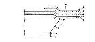
l Fig. 1 is a sectional view of a constitution
of a cantilever and leader electrodes. The cantilever
portion is constituted of a piezoelectric material
layer 5, 7 and driving electrode layers 4, 6, 8. At
the free end of the cantilever, a tip 9 is provided.
The electrode for leading out the tunnel current is
formed simultaneously with the formation of the upper
electrode 8. The intermediate and upper electrodes 6,
8 are wired over a long distance practically to a
bonding pad, although they are shown to be cut in the
drawing.
The constitution and the effect of the present
invention are described by reference to the drawing of
a production flow in Figs. 2A to 2C. As shown in Fig. 2A,
since a thick film can readily be formed on a (100) Si
substrate, silicon oxide films 3 are formed thereon in
a thickness of 1 ~m or more in a thermal oxidation
furnace. The both faces are subjected to patterning.
In the patterning, the silicon oxide films on both
surfaces are left remaining only on the supporting
portion 13. The patterning of the silicon oxide film
3 is conducted preferably by isotropic etching with an
aqueous HF solution or the like because the coverage
of the lower electrode 4 to be formed later will
become insufficient if the end of the edge portion 12
of the silicon oxide film is steep and the lower
2069708
- 11 -
l electrode 4 to be formed in the step of Fig. 2C is
relatively thin. Thereafter, silicon nitride films 2
are formed in a thickness of from 1000 to 1500 A by
vapor growth of an SiH2Cl2 gas and an NH3 gas, and the
film at the back side only is patterned. Instead of
formation of the silicon nitride films, silicon oxide
films may be formed again by means of a thermal
oxidation furnace. Subsequently, etching is conducted
by anisotropic etching of Si, for example by heating
with an aqueous KOH, at the region of the cantilever
portion to form an Si membrane 10 of several ten ~m
thick as shown in Fig. 2B. Thereafter, a lower
electrode 4 of about 1000 A thick and a piezoelectric
material layer 5 are formed as shown in Fig. 2C. In
the same manner, an intermediate electrode 6, another
piezoelectric material layer 7, and an upper electrode
8 are laminated in this order. Further thereon, a tip
9 is formed. After the resulting matter is coated in
a thickness of 10 ~m or more, the Si membrane 10 and
the silicon nitride film are removed by anisotropic
etching with an aqueous KOH solution or the like or by
plasma etching with a gas such as CF4 and SF6.
Further the coating is removed off by plasma etching
with a gas such as CF4 and SF6. Thus a cantilever
having constitution as shown in Fig. 1 is obtained.
The advantage of the above constitution of the
2069708
- 12 -
l present invention are as below. In the traditional
constitution of Fig. 6, as described above, undesired
parasitic capacitances, c1 and c2, are induced as
shown in the equivalent circuit shown in Fig. 7, where
c denotes the capacitance of the piezoelectric
material; r1 and r2 denote resistances of wiring; and
r3 denotes the resistance of the substrate.
The values of c, c1, and c2 of the present
invention (Fig. 1) are compared with the ones of prior
10 art (Fig. 6) under the conditions below.
Conditions
Thickness of SiO2,3 (Present invention) 1,um
Thickness of Si3N4,2
(Insulating layer in prior art) 0.15 ,um
Thickness of piezoelectric material layer, 5, 7
0.3 ,um
Dimension of cantilever 9 - 300 ~m X lOO ~m
Wiring 5 ~m wide X 5 mm long
Dielectric constant of Si3N4 -11
Dielectric constant of SiO2 3 5 x 10-11 (F/m)
Dielectric constant of ZnO 1.1 x lO ~ (F/m)
Parasitic capacitance
Prior art Present invention
c 11 pF 11 pF
c1 16.5 pF 0.7 pF
C2 5.9 pF 0.7 pF
2069708
- 13 -
l c' 4.3 pF 0.4 pF
(c' being the total of cl and c2)
As shown above, in the cantilever of prior
art, the ratio of the parasitic capacitance to the
capacitance of the main body of the cantilever (c'/c)
is about 40 %, while the value of c' of the present
invention is as low as 1/10 or lower thereof. In the
case of a multi-probe shown in Fig. 4, the wiring
length differs among the probes, which causes large
differences in the parasitic capacitances of the
probes and in the resistance of the substrates, thus
causing variation ln cantilever driving. On the
contrary, in the cantilever of the present invention,
the variation of the parasitic capacitance caused by
the variation of length of the wiring is reduced
because the parasitic capacitance is low. In other
words, the present invention enables reducing greatly
the variation of the characteristics among the
respective cantilever.
Example 2
Another process for the production of a
cantilever in described below by reference to Fig. 3.
The basic constitution and effects of this Example are
the same as those in Example 1.
On both faces of an Si substrate 1,
respectively silicon nitride films 2 are formed by
2069708
- 14 -
l reaction of SiH2C12 and NH3 at about 800~C in a
thickness of from 100 to 1500 A by means of an LPCVD
apparatus. The silicon nitride film on the back side
is subjected to patterning and etching for formation
of an Si membrane region 10. Then a silicon oxide
film 3 is formed only at the front face by reaction of
SiH4 and ~2 by means of a normal-pressure CVD
apparatus, and the resulting film is patterned and
etched to obtain constitution as shown in Fig. 3. The
subsequent procedure is the same as in Example 1.
Incidentally, the same result is obtained by
forming the Si membrane 10 before the formation of the
silicon oxide film 3.
Example 3
A recording-reproducing apparatus which
employs the above probe-driving mechanism is described
below as an example of the information-processing
apparatus of the present invention. Fig. 5
illustrates roughly a recording-reproducing apparatus
of the present invention. On a silicon substrate 101,
the probe-driving mechanism 102 of the present
invention is provided in plural numbers. A
piezoelectric element 105 for coarse driving drives
the silicon substrate in the Z direction. The numeral
103 denotes a plate-shaped recording medium. Data
lines 104 are formed by arranging, in lines, recording
~ 2 ~ ~ ~ 7 ~ 8
_ - 15 -
l areas determined by a scannable region of the probe-
driving mechanism. The recording medium 103 is moved
by a movement mechanism, not shown in the drawing, in
parallel in a direction indicated by the arrow mark in
the drawing, and information is written into the
recording areas in lines. The probe-driving mechanism
102 and the piezoelectric element 105 for Z-direction
coarse-driving are constituted so as to be movable in
a direction perpendicular to the data lines by means
of a movement mechanism such as a linear motor not
shown in the drawing. Thereby any desired data line is
accessed to record and reproduce the data. The access
to the desired data line is conducted by a position-
detecting device such as a linear encoder.
Thereafter, each of the probes of the probe-driving
mechanism 102 scans the respective recording areas of
the intended data lines.
The recording layer 103 may be made of a
material exhibiting a memory-switching phenomenon (or
electric memory effect) in current-voltage
characteristics, such as an organic monomolecular film
or a built-up film thereof prepared by laminating on
an electrode molecules comprising both a group having
a ~ electron level and a group having only a
electron level as described in Japanese Patent
Application Laid-Open No. Sho-63-161552. The electric
2069708
- 16 -
1 memory effect enables reversible transition (or
switching) between two or more electroconductive
states (ON state and OFF state in Fig. 8), namely a
low-resistance state (ON state) and a high-resistance
state (OFF state) of a thin film such as the
aforementioned organic monomolecular film or a built-
up film thereof placed between a pair of electrodes by
application of a voltage exceeding a threshold value.
The respective states can be retained (or memorized)
without application of a voltage.
The recording medium 103 may also be made of a
material which changes the surface state to be convex
or concave by local melting or local evaporation by
application of a voltage higher than a threshold
value, such as a metal film of Au or Pt, and the like.
The method of recording and reproduction is
described below.
The recording is conducted by moving the Z-
direction coarse-movement piezoelectric element 105
and the probe-driving mechanism 102 by a movement
mechanism to a recording position and then applying a
voltage exceeding a threshold value onto the recording
medium 103. At that time, a bias voltage is applied
to the recording medium 103 by a bias circuit 106, and
the probes are held at a distance from the recording
medium to allow a tunnel current to flow. The probes
2069708
- 17 -
l are brought close to the recording medium by the Z-
direction coarse-movement piezoelectric element 105,
and then respective probes are brought into the tunnel
region by the probe driving mechanism 102. The probe
is kept at a predetermined distance from the recording
medium by feedback of the tunnel current, which is
detected by the tunnel-current-detecting circuit 107,
through the Z-direction serve circuit 110 of the
respective probe-driving mechanism. In the Z-
direction servo circuit 110, a low-pass-filter is
provided, and the cut-off frequency is selected so as
not to follow the data signal but to follow the swing
of the recording medium and waves on the recording
medium, thereby the average distance between the probe
and the recording medium is controlled to be constant.
At the time of recording, the recording
signals are sent from a control circuit 112 to a pulse-
applying circuit 108, thereby pulse voltage being
applied to respective probes to conduct recording. In
the Z direction servo circuit 110, a hold circuit is
provided and driving voltage of the probe-driving
mechanism 102 to which pulse voltage is applied is
maintained so that the pulse application may not cause
change of the distance between the probe and the
recording medium. Thereby, recording bits are
recorded in a matrix form in the recording area of the
2069708
- 18 -
l data lines 104. In the respective recording lines,
address information is inserted, which enables
discrimination of date on reproduction.
The reproduction is conducted as below.
In reproduction, the probe is moved to the
recording area of the desired data line 104, and the
difference of the tunnel current flowing between the
recording medium 103 and the probe at the recorded
portion from that at the non-recording portion is
detected. The probe-driving mechanism 102 is
controlled by an XY position-controlling circuit 109
so that the probe scans the entire recording area.
The reproduction signal in one recording area is
passed through a tunnel-current-detecting circuit 107
and is stored temporarily by signal processing in the
control circuit 112. Therefrom, desired data only is
reproduced and outputted.
In such a recording-reproducing apparatus, the
probe-driving mechanism having the constitution of the
above Example broadens the region which is scannable
with one probe, making one recording area larger, and
raising the recording density as a whole.
Example 4
An STM apparatus was prepared by use of a
cantilever type probe of Example 1. The block diagram
of the apparatus is similar to the one of Fig. 5.
2069708
- 19 -
l With this apparatus, a cleavage face of
substrate of HOPG (highly oriented pyrolysis graphite)
was observed at the bias current of 1 nA, and the
scanning area of 100 A X 100 A, thereby a satisfactory
atomic image being obtained.
The surface of the HOPG substrate having small
steps was observed in the same manner as above at a
scanning area of 500 A X 500 A . Thereafter the probe
is once removed from the substrate, and then the
observation was conducted again, thereby the steps on
the surface being observed at the same positions with
satisfactory reproductivity.
Example 5
A set of a piezoelectric actuators for an ink-
jet head was prepared by juxtaposing a plurality ofactuators. The sectional view and the perspective
view thereof are roughly illustrated in Fig. 9A and
Fig. 9B, respectively.
The piezoelectric actuators were prepared in
the same manner as Example 1 immediately before the
removal of the substrate except that the tips were not
formed. Subsequently, a plurality of nozzle openings
29 were formed on a substrate 28 for nozzles.
Further, spacers 27 were formed. The spacers 27 were
made of an electroconductive thin plate of a noble
metal or the like. The spacers connect upper
- 20 - A ~ 7 ~ 8
l electrode 8 and also serve as leader
electrodes. Each lower electrode of the respective
piezoelectric actuators was connected to a leader
electrode, not shown in the drawing, to apply voltage
individually. After registration, the substrate 1
having the piezoelectric actuators and the nozzle
substrate 28 were glued together. Finally the
substrate at the portions below the piezoelectric
actuator was eliminated by anisotropic etching with an
aqueous potassium hydroxide as shown in Example 1
except the one side of the end portions of the
piezoelectric actuators.
The ink-jet head thus prepared is capable of
ejecting ink through the nozzle opening 29 by
displacing vertically the free end of the
piezoelectric actuator caused by the voltage applied
to the lower electrode 4 and thereby increasing the
pressure of the ink in the vicinity of the nozzle
opening 29. By use of a plurality of actuators to
which voltage is applied as above selectively and
intermittently, desired printing is practiced with
satisfactory responsibility to the voltage
application.
In the present invention, the insulating layer
between the substrate and the electrode of the
cantilever is left remaining only under the wiring
2069708
- 21 -
l portion on the substrate, and thereafter the electrode
layer and the piezoelectric layer are laminated.
Therefore, the problem of undesired side etching of Si
does not arise in the etching of the insulation layer
subsequent to the etching of the Si membrane at the
cantilever portion. Accordingly, the insulating layer
under the wiring can be made thick and thereby the
parasitic capacitance between the wiring portions can
be decreased, and the rigidity of the cantilever
portion can be lowerd. Thus the variation in
parasitic capacitances among the probes can be made
low, and the values of the parasitic capacitances can
be made small, whereby the controllability of the
probe driving is remarkably improved. In addition,
the driving characteristics of the cantilever is
improved.