Note: Descriptions are shown in the official language in which they were submitted.
2069~90
RF POWER AMPLIFIER
BACKGROUND OF THE INVENTION
The present invention relates to a radio frequency
(RF) power amplifier for amplifying an RF signal with a
high power efficiency and with a minimum of distortions
by use of a GaAs field effect transistor (FET) and, more
particularly, to an RF power amplifier feasible for the
power amplification of an ON/OFF RF signal, e.g., TDMA
(Time Division Multiple Access) signal to be sent from
a digital portable telephone.
It has been customary with the above-described type
of RF power amplifier to use amplification, i.e., class
"AB" or class "B" amplification for the purpose of enhancing
the radio of RF signal output to supplied DC power, i.e.,
a power efficiency. Specifically, with such an RF power
amplifier, it is a common practice to reduce the drain
current, or idling current, of the FET to less than
about one-tenth of saturation drain current (class "AB"
amplification) when an RF signal is not inputted or
when a small RF signal is inputted. When an RF signal
of regular level is inputted to the RF power amplifier
(generally during high amplitude operation), the drain
current of the FET sharply increases even to a level four
or five times higher than the idling current. Nevertheless,
a high power efficiency is achievable since the gain and
206999~
RF signal output in such a condition increase more than
the drain current.
However, the problem with the RF power amplifier is
that the nonlinear amplification mentioned above noticeably
distorts the RF signal output due to, among others,
intermodulations (particularly odd intermodulations, e.g.,
IM3, IM5 and IM7). For example, when a digital signal
modulated by QPSK (Quadrature Phase-Shift Keying) is
applied to the RF power amplifier, the distortion of
the RF signal output is, when evaluated in terms of
nearby channel leak power, found to increase beyond a
limit regarding the specifications of a system using the
QPSK modulated wave.
In this connection, one of conventional RF power
amplifiers of the type performing class "AB" amplification
with an FET uses a module FM C090902 (manufactured by
Fujitsu Ltd., Kawasaki, Japan) and applies a voltage of
5.8 V to between the drain and the source of the FET to
thereby cause an idling current of 150 mA to flow. When
an RF signal of 950 MHz and +3 dBm is inputted to such
a power amplifier, an RF signal output of +32 dBm (gain
of 29 dB) and an FET drain current of 600 mA are obtained,
insuring a satisfactory power efficiency. However, the
50 kHz nearby channel leak power of this module is as
great as 35 dB in terms of RF signal output ratio.
~ 3 ~ 2069990
SUMMARY OF THE INVENTION
It is therefore an object of the present invention
to provide an RF power amplifier which reduces inter-
modulation distortion ascribable to class "AB" or class "B"
amplification, specifically an RF power amplifier capable
of amplifying an RF signal with a higher power efficiency
and with a minimum of signal distortions by use of an FET.
It is another object of the present invention to
provide an RF power amplifier suitable for the power
amplification of a TDMA signal or similar ON/OFF RF signal.
An RF power amplifier of the present invention has a
power amplifier unit for amplifying an RF signal from an
RF signal source by an FET included therein and delivering
the amplified RF signal to a load, and a drain bias control
circuit for turning on and turning off a drain bias to the
FET in synchronism with the turn-on and turn-off of the
RF signal. The power amplifier unit includes an input
low pass filter (LPF) connected to the gate electrode of
the FET and an output LPF connected to the drain electrode
of the FET. The LPFs each matches the FET and the RF
signal source or the FET and the load with respect to
impedance and power. The power amplifier unit includes
a drain bias circuit for applying a drain bias to the
drain electrode of the FET, and a gate bias circuit for
applying a gate bias to the gate electrode of the FET.
The input terminal of the drain bias circuit is connected
to the output terminal of the drain bias control circuit.
2069990
-- 4 --
In the RF power amplifier unit, an idling current for
class "A" amplification flows through the FET. The power
amplifier unit substantially matches the dynamic impedance
Zd of the FET and the load impedance Zl by the output LPF
when a regular RF signal is outputted (i.e. assuming that
the impedance of the output LPF is zf, zf2 Zd- Zl is
set up). Specifically, the power amplifier unit sets the
output LPF impedance Zf such that substantially the maximum
power is applied from the FET to the load when a regular
RF signal is outputted, i.e., such that the FET and the
load are matched in power. Let the output LPF impedance
Zf satisfying the above-mentioned power matching condition
be referred to as a power matching impedance Zm herein.
Generally, the dynamic impedance of an FET increases with
the increase in RF signal input level. Therefore, the
output LPF impedance Zf is made higher than an impedance
which will give substantially maximum gain during low RF
signal level operation (referred to as a high gain
impedance Zg hereinafter) and set at the power matching
impedance Zm. Then, since the output LPF impedance Zm
is higher than the high gain impedance Zg, the drain
current of the FET when a regular RF signal is outputted
is smaller than when the output LPF impedance Zf is set
at the high gain impedance Zg. The RF power amplifier,
therefore, achieves a high power efficiency in the event
of regular RF signal output despite the class "A"
amplification which distorts signals little.
- 2069990
In the event of amplifying a TDMA signal or similar
ON/OFF RF signal, the RF power amplifier turns on and turns
off the drain bias to the FET in synchronism with the turn-on
and turn-off of the RF signal. The amplifier, therefore,
prevents the drain current from appearing in the FET when the
RF signal is in an OFF state, thereby saving power. Moreover,
the amplifier frees the RF signal output from noticeable
distortions and is, therefore, feasible for the power
amplification of, among others, a TDMA signal or similar
digital RF signal which occurs in bursts with a constant
level.
The power amplifier unit may be provided on a thick
film substrate in a hybrid integrated circuit (IC)
configuration to reduce the size of the RF power amplifier.
If the input and output LPFs are each implemented by chip
capacitors and inductors of a distributed constant circuit,
the scattering between them will be reduced to facilitate the
fabrication of the RF power amplifier.
According to a broad aspect, the invention provides
a radio frequency (RF) power amplifier comprising: a field
effect transistor ~FET) for amplifying an RF signal applied to
a gate electrode thereof to thereby output an amplified RF
signal via a drain electrode thereof; drain bias applying
means for applying a drain bias to said drain electrode of
said FET; gate bias applying means for applying a gate bias to
said gate electrode of said FET, said drain bias applying
means and said gate bias applying means setting an idling
current for class "A" amplification in said FET; an output low
!. 5
66446-542
2069990
pass filter ~LPF) disposed between an RF signal output
terminal to which a load is connected and said drain electrode
for matching said FET and said load with respect to power,
said output LPF having an impedance higher than an impedance
which gives said RF power amplifier substantially the maximum
gain when said RF power produces a regular output; and bias
application control means for turning on and turning off the
application of the drain bias to said drain bias applying
means in synchronism with the turn-on and turn-off of the RF
signal.
BRIEF DESCRIPTION OF THE DRAWINGS
The above-mentioned and other objects, features and
advantages of the present invention will become more apparent
from the following detailed description when taken in
conjunction with the accompanying drawings, wherein:
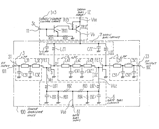
FIG. 1 is a circuit diagram representative of an RF power
amplifier embodying the present invention;
- 5a -
., ~.
~'
66446-542
~ - 6 - 2069990
FIG. 2 is a graph indicative of the static
characteristic of an FET included in the embodiment; and
FIG. 3 shows the waveforms of an input RF signal Sl
and a drain bias VD particular to the embodiment.
DETAILED DESCRIPTION OF THE PREFERRED EMBODIMENT
Referring to FIG. l of the drawings, an RF power
amplifier embodying the present invention is shown and
includes a power amplifier unit 100 implemented as a thick
film hybrid IC. The power amplifier unit 100 has an RF
signal input terminal 101 to which an RF signal Sl is
applied from an RF signal source, not shown. FETs 1 and 2
amplify the input RF signal Sl to feed the resulting RF
signal output S3 to a load, not shown, via an RF signal
output terminal 102. It is to be noted that the input RF
signal Sl may be a TDMA signal undergone QPSK modulation,
and that the impedances Za and Zl of the RS signal source
and the load, respectively, are usually 50 Q. A drain
current control circuit 103 selectively turns on or turns
off a drain voltage VDD from a drain bias input terminal
12 by a switch circuit; in an ON state, the control
circuit 103 feeds a drain bias VD to a drain bias circuit
7 included in the power amplifier unit 100 via the output
terminal thereof. Specifically, the drain current control
circuit 103 receives a control signal Sc synchronous with
the ON/OFF of the input RF signal Sl via a control signal
input terminal 11 thereof and, in turn, controls the switch
- 7 - 2069990
circuit by the control signal Sc to turn on and turn off
the supply of the drain bias VD to the drain bias circuit 7.
In the power amplifier unit 100, an input LPF 3 is
disposed between the RF s ignal input terminal 101 and the
gate electrode of the FET 1 in order to set up impedance
matching between the RF s ignal source and the FET 1. An
interstage LPF 4 is connected between the drain electrode
of the FET 1 and the gate electrode of the FET 2. This
LPF 4 plays the role of an impedance matching circuit for
the FETs 1 and 2 and the role of gain matching circuit for
increasing the gain of the FETs 1 and 2 at the same time.
An output LPF 5 is connected between the drain electrode
of the FET 2 and the RF signal output terminal 102 for
matching the dynamic impedance Zd of the FET 2 associated
with the output RF signal S3 of regular level and the load
impedance Zl, i.e., matching the FET 2 and the load with
respect to power. The drain bias circuit 2 delivers the
drain bias VD fed from the output terminal of the drain
bias control circuit 2 to the drain electrodes of the
FETs 1 and 2. A gate bias circuit 6 receives a gate
voltage VG0 applied to a gate bias input terminal 61 and,
in turn, generates gate biases VGl and VG2 for the FETs
1 and 2, respectively. The gate biases VGl and VG2 are
applied to the gate electrodes of the FETs 1 and 2,
respectively.
In detail, the input LPF 3 has a cut-off frequency
far higher than the frequency of the input RF signal Sl
-- 8 --
2069990
and is made up of inductors L31 and L32 of a distributed
constant circuit, and chip type capacitors C31 and C32.
The distributed constant circuit is constituted by a 50Q
line shorter than the wavelength of the input RF signal Sl.
Preferably, the impedance Zfl of the LPF 3 should be set
such that the impedance Zs of the RF signal source and
the input impedance Zil of the FET 1 match at the regular
input level of the input RF signal Sl.
The LPF 5 also has a cut-off frequency far higher
1~ than the frequency of the input RF signal Sl. The LPF 5
has inductors L51 and L52 of a distributed constant circuit,
and chip type capacitors C51 and C52; the distributed
constant circuit is implemented by a 50 Q line shorter
than the wavelength of the input RF signal Sl. The
impedance Zf 3 of the LPF 5 iS selected to be nearly equal
to (Zd. Zl)l/2 so as to increase the power efficiency of
the FET 2, i. e., to match the FET 2 and the load in power
at the regular output level of the output RF signal S3
and within a range which does not aggravate the signal
distortion of the RF signal S3.
The interstage LPF 4, like the above-stated LPFs,
has a cut-off frequency far higher than the frequency of
the input RF signal Sl and is constituted by inductors
L41, L42 and L43 of a distributed constant circuit, and
chip type capacitors C41 and C42. The distributed constant
circuit is implemented by a 50 Q line shorter than the
wavelength of the input RF signal Sl. The impedance
- 9 2069990
setting condition of this LPF 4 is intermediate between
the impedance setting conditions of the LPFs 3 and 5.
However, since the level of the output RF signal of the
FET 1 (input RF signal of the FET 2) is far lower than
that of the output RF signal S3, the impedance Zf3 of
the interstage LPF 4 should preferably be so set as to
increase the gain of the RF signals Sl and S2 while
reducing signal distortions.
The drain bias circuit 7 delivers the drain voltage VD
from the output of the drain current control circuit 103
to the drain electrode of the FET 1 via the inductor L21
and to the drain electrode of the FET 2 via the inductor
L22. The chip type capacitor C21 and inductor L21 and
the chip type capacitor C22 and inductor L22 respectively
cooperate to prevent the RF signals S2 and S3 from leaking
from the power amplifier unit 100 to external circuitry
including the drain current control circuit 103.
The gate bias circuit 6 divides the gate voltage VGo
from the gate bias input terminal 61 by resistors R62 and
R62 and thereby feeds an adequate gate bias VGl to the
gate electrode of the FET 1 via an inductor L61. At the
same time, the circuit 6 divides the gate voltage VGo by
resistors R63 and R64 to apply an adeuate gate bias VG2
to the gate electrode of the FET 2 via an inductor L62.
The inductors L61 and L62 respectively cooperate with
chip type capacitors C61 and C62 to prevent the RF signals
-- 10 --
2069990
Sl and S2 from leaking from the power amplifier unit 100
to the external circuitry.
The drain current control circuit 103 passes the
drain voltage VDD from the drain bias input terminal 12
through a switching bipolar transistor TR12 and then
feeds the drain bias VD to the drain bias circuit 2 via
the output terminal thereof (collector electrode of the
transistor TR12). The ON/OFF signal (control signal) Sc
from the control signal input terminal 11 is applied to
the base electrode of a control bipolar transistor TRll
while a signal responsive to the signal Sc is applied to
the base electrode of the transistor TR12 to thereby switch
on or switch off the transistor TR12. As a result, the
supply of the drain bias VD to the drain bias circuit 7
is set up or interrupted under the control of the control
signal Sc. Resistors Rll and R12 respectively set biases
for the base electrode and the emitter electrode of the
transistor TRll. Likewise, a resistor R13 sets a bias
for the base electrode of the transistor TR12.
The operation and circuit constant setting of the
power amplifier unit 100, particularly the FET 2 and
output LPF 5, will be described with reference also made
to FIG. 2.
To begin with, to set an idling current Idi which
causes the FET 2 to perform class "A" amplification,
the drain bias circuit 7 and the gate bias circuit 6
- 11- 2069990
respectively set the drain bias VD and the gate bias VG2
in the FET 2. Assuming that the saturation drain current
of the FET 2 is Idss, then the idling current Idi during
class "A" amplification (i.e. drain current Id2) lies in
the range of 0.2Idss to 0.6Idss. When it is desired to
increase the power efficiency of the power amplifier unit
100, the drain current Id2 is set at the power limit, i.e.,
about 0.2Idss. The gate bias VG during class "AB"
amplification is VGl which is deeper than the gate bias
VG2 assigned to class "A" amplification, so that the
idling current Idi (drain current Idl) is reduced to
about O.lIdss. The idling current Idl which minimizes
the signal distortion is about 0.5Idss. The impedances
Zf2 and Zf3 of the interstage LPF 4 and output LPF 5 are
respectively set at high gain impedances Zg2 and Zg3
beforehand, so that in the initial stage of circuit
constant setting the FETs 1 and 2 may each generate
substantially the maximum gain in response to a small
input RF signal.
Next, the input RF signal Sl is applied to the RF
signal input terminal 101, i.e., the RF signal S2 is
applied to the gate electrode of the FET 2. As a result,
the output RF signal S3 of regular level appears on the
RF signal output terminal 102. At this instant, the drain
current Id of the FET 2 is substantially the same as that
of an FET of class "AB" amplification. The impedance Zf3
- 12 - 2 0 69 9 9 0
of the output LPF 5 is adjusted such that the drain current
Id of the FET 2 decreases with the regular output level
being maintained. Specifically, since the dynamic
impedance of the FET 2 increases with the increase in the
level of the RF signal S2 coupled to the gate electrode
thereof, to adjust the circuit constant of the output
LPF 5 in a direction for reducing the drain current of
the FET 2 means to increase the impedance Zf3 of the LPF 5
to above the previously mentioned high gain impedance Zg3.
As the impedance Zf3 increases to the power matching
impedance Zm nearly equal to (Zd . Zl)l/2, the power
amplifier unit 100 achieves substantially the maximum
output level despite that the drain current Id of the
FET 2 is smaller than when the impedance Zf3 of the
output LPF 5 is set at the high gain impedance Zg.
Conversely, when the impedance Zf3 of the output LPF 5
is set at the power matching impedance Zm, the output RF
signal S3 will have the same level as the level corresponding
to the high gain impedance Zg3 even when the drain current
Id is lowered to below 90 %. It is noteworthy that the
distortion of the output RF signal S3 remains the same as
when the high gain impedance Zg3 is set, since the class
"A" amplification bias is not set on the drain electrode
or the gate electrode of the FET 2.
As stated above, with the power amplifier unit 100,
it is possible to set up a high power efficiency by
- 13 - 2069990
selecting the impedance Zf3 of the output LPF 5 higher
than the high gain impedance Zg3. In addition, class "A"
amplification is not degraded despite a low drain current
Id, freeing the output RF signal S3 from distortions.
In the power amplifier unit 100, the FETs 1 and 2
may respectively be implemented by NE800196 (manufactured
by NEC Corp., Tokyo, Japan; Idss of 300 mA) and N1069L-4B
(also manufactured by NEC Corp.; Idss of 3A), and a drain
voltage VD of 5.8 V can be applied to the drain electrodes
of the FETs 1 and 2. In such a power amplifier unit 100,
when the impedance Zf3 of the output LPF 5 was set at the
high gain impedance Zg3 and an RF signal Sl of 960 MHz
was inputted, an output RF signal S3 of 32 dBm, a total
drain current of 618 mA (about 0.19 Idss) of the FETs
1 and 2, a gain of 28 dB, and 50 kHz nearby channel leak
power of -48.5 dB were obtained. On the other hand, when
the impedance Zf3 of the output LPF 5 was set at the power
matching impedance Zm, the total drain current, the gain
and the 50 kHz nearby channel leak power were respectively
measured to be 566 mA, 27 dB and -49.3 dB on the assumption
that the output RF signal S3 had the level of 32 dBm as
in the above-mentioned case. In this way, for the same
nonlinear distortion, the power amplifier unit 100 whose
output LPF 5 has the impedance Zf3 thereof set at the
power matching impedance Zm reduces the total drain
current to about 90 % of the drain current associated
- 14 - 2069990
with the high gain impedance Zg3. In the power amplifier
unit 100, the idling current Idi is much greater than in
the previously stated conventional class "AB" power
amplifier. However, when the unit 100 is turned on in
response to a regular RF signal Sl, the power consumption
remain substantially the same (decreases by about 6 %)
while the 50 kHz nearby channel leak power is reduced by
more than 10 dB.
Referring also to FIG. 3, the input RF signal Sl
appearing on the RF signal input terminal 101 is a TDMA
signal having an ON period Ton and an OFF period Toff
which are respectively one- third and two- third of the
entire signal period. The ON period has a preamble signal
period Tp at the beginning and a guard period Tg at the
end. The control signal Sc synchronous with the input RF
signal Sl is applied to the control signal input terminal 11.
In response, the gate current control circuit 103 turns off
or turns on the drain bias VD to the drain bias circuit 7.
The turn-on and turn-off of the drain bias VD occur in the
preamble signal period Tp and guard period of the input RF
signal Sl. The power amplifier unit 100 maintains the
normal RF signal output S3 throughout the data signal
period except for the periods Tp and Tg. It follows that
the power amplifier unit 100 is turned on and turned off
in synchronism with the turn-on and turn-off of the RF
signal Sl and, therefore, achieves a power efficiency even
2069990
higher than that of a continuously operating class "AB"
power amplifier. Moreover, the unit 100 is feasible for
the power amplification of a TDMA signal since it operates
only in the class "A" amplification mode which scarcely
distorts signals.
In summary, in accordance with the present invention,
the RF power amplifier causes the FETs 1 and 2 to operate
in the class "A" amplification mode and selectively turns
on or turns off the drain bias VD to the FETs 1 and 2 in
synchronism with the input RF signal. Hence, when an RF
signal of regular level is inputted to the RF power
amplifier, the amplifier achieves a high power efficiency
and allows a minimum of nonlinear distortions, particularly
intermodulation distortion, to occur. It follows that
when the RF power amplifier is used to amplify the power
of, for example, a TDMA signal undergone QPSK modulation,
it not only enhances the power efficiency, compared to a
conventional RF power amplifier, but also reduces the
nearby channel leak power by more than 10 dB.
Although the invention has been described with
reference to the specific embodiments, this description
is not meant to be construed in a limiting sense. Various
modifications of the disclosed embodiments, as well as
other embodiments of the invention, will become apparent
to persons skilled in the art upon reference to the
description of the invention. It is therefore contemplated
- 16 ~ 20 69990
that the appended claims will cover any modifications or
embodiments as fall within the true scope of the invention.