Note: Descriptions are shown in the official language in which they were submitted.
- 1- 2070178
CAPACITIVE POWER SUPPLY
Background of the Invention
The present invention relates generally to power supplies, and,
more particularly, to a portable, capacitive power supply for powering
20 a load element, such as a portable radiotelephone.
Portable power supplies are utilized to power many varied
electrical devices. In many instances, the use of such a portable
power supply to power an electrical device is necessitated in instances
in which the electrical device cannot be positioned proximate to a
25 perm~nent power supply to be supplied power the~e~lvm. In other
inP~nces~ the use of a portable power supply to power an electrical
device is advantageous as the portable power supply enhances the
portability of the electrical device. A portable power supply may be
positioned pro~imate to the electrical device, or carried with, or
30 within, the electrical device. The electrical device need not be
positioned proximate to a permanent power supply to permit
operation of the electrical device, and power cables connecting the
electrical device with the permanent power supply are not required.
.
-2- 2070178
Conventionally, portable power supplies are compri~ed of
ele~,r~hemiç~l materials. Energy is stored in the electrochamical
material in the form of çh~mi~l energy, and, conversion of the
chemical energy into electrical energy caused by reaction of the
5 electrorhamical msterial, provides the power to power the electrical
device thereby.
Such conventional, portable power supplies are generically
lafer.ed to as batteries, and are widely popular both for re~on~ of
av~ hility, convçniance~ and initial purchase price. A battery,
10 how~v~r~ (as is also true with other types of portable power sources),
is of a limited energy storage capacity. When a battery is coupled to
an electrical device and ~ ;li7e-l to power the electrical device thereby,
the stored energy contained in the battery is CO11Vel led into electricsl
energy and rli~çh~rged therefrom.
After an çYt~n~le~l period of use, ~ ch~rge of the stored energy
of the battery ~?pletes the battery of ram~ining stored energy. Once
the stored energy of the battery is ~leplete~ below a certain level,
replr^çmçnt of the battery is necçssitated to permit continued
operation of the electrical device. The frequency with which the
20 battery must be replaced i8, of course, dep~n~lant upon the battery
capacity (i.e., the amount of energy stored in the battery), the energy
required to operate the electrical device, and the frequency with
which the electrical device is operated.
Nickel-cadmium (M-Cd) batteries have been developed and are
25 widely used as portable power sources for the reason that a Ni-Cd
battery, once depleted of stored energy, may be recharged simply by
cQnnect;ng the battery to a suitable charging current source for a
period of time. Other battery types have ~imil~rly been developed
which may be recharged once depleted of stored energy. Battery
30 charging appsratus is also known and available to permit such
recharging.
However, a rechargeable battery csnnot be recharged and
reused an unlimited number of times. For instsnce, a Ni-Cd battery
may be typically recharged up to appro~im~tely five hundred times.
~3~ 207017~
After repeated recharging of the Ni-Cd battery, conversion of the
energy of a charging current applied to the battery into stored,
chemical energy of the battery is much less efficient. Eventually,
efficiency of energy conversion becomes 80 low that the battery does
5 not become recharged to a significant extent. Therefore, even a
rechargeable battery has a limited, procti~-o-l life.
Additionally, when recharging a rechargeable battery, the rate
at which a charging current is applied to the battery must be
controlled to ~ lt ~3-o-mage to the battery. More particularly, the
-- 10 charging current applied to the battery must be less than a certain,
m~ .... level. Rec~l~Ae the level of the charging current applied to
the rechargeable battery determines the charging rate of the batter~r,
the time required to recharge a battery cannot be reduced below a
time period which is depen~lpnt upon the m~Yimum current level
that may be applied to the battery. Such a minimllm time period
lcqui~ed to recharge a rechargeable battery, can pose inconveniences
For in~once, if only one rechargeable battery is av~ilo-hle to power the
electrical device, the electrical device cannot be operated prior to
espiration of the time period required to recharge the battery.
Still further, when charging a rechargeable battery, such as a
Ni-Cd battery, at a m-oyimum~ . llowable charging rate (to minimi~e,
thereby, the time period required to recharge the battery), application
of the charging current to the battery must be termin-o-te~l once the
battery becomes ~lly charged. Overcharging of the battery at the
m~Yimum allowable charging rate can cause ~ssing~ electrolytic
venting of the battery, perm~n~nt 1088 of battery capacity, and
physical ~mage to the battery.
CAp~^itors used to form portable power sour~s for low power
applications are also known. For PY~mple~ capacitive power sources
have been utilized as backup power supplies for integrated circuit
memories. Capacitors having capacitances of values great enough to
generate current levels to power most electrical devices for ext~n~le~
periods of time, however, have heretofore been impractical for the
reason that such capacitors were of ~ignific~nt tlimpn~ions. Other of
-4- 2070178
such capacitive power sources are of very high effective resistances,
and are simil~-ly impractical for use to generate large current levels.
One electrical device which is o~entimes powered by a portable
power supply is a portable transceiver, such as a radiotelephone
S llt;li7e l to commllnir~ts in a cellular, communication system. When
po.. e~ed by a portable power supply, the radiotelephone may be
positioned at any loc~t;~n throughout a geogr~phic~l area
çncomp~cse-l by the cellular, commllnic~t;on system.
Operation of the radiotelephone, ho~. ever, typically requires
10 powering of the radiotelephone at a power of up to three watts. Such a
power requil~ ent requires a relatively large battery (both in size and
weight) to permit ext9ntip~l operation of the radiotelephone. How~ver,
to enh~nre the portability of the radiotelephone, the battery should be
of minim~l size and weight. Battery size considerations responsive to
15 such power requirçm~nt~ and the design goal of size and weight
minimi7~t;on conflict. Existing rechargeable battery tiesign~
compromise between energy storage capacity and battery size. One
commercially av~ ble~ rechargeable battery is of a ~le~i~n which
u,its ~OWe~ of a r~iiotelephone at a power level of three watts
20 for a period of a~plo~;...~tely one and one half hours, and is of a
weight of less than six ollnC~
To operate the radiotelephone for an eYte ~ie~l period of time
(i.e., beyond the time period per_itted by the energy storage capacity
of the battery), a radiotelephone user typically carries a spare, and
25 freshly charged, battery in addition to the primary battery initially
ll~ili7e-1 to power the radiotelephone. Once the primary battery
h~ec~...es ~lisrh~rged to a level l~reventing further operation of the
radiotelephone, the battery is replaced with the spare battery to
per_it, thereby, continued operation of the radiotelephone.
The radiotelephone user may be required to carry more than
one spare battery to further extend the period of operation of the
radiotelephone if the primary battery cannot be recharged before the
spare battery becomes ~ rh~rged.
2070178
Even when a radiotelephone user has access to battery
charging apparatus, if the time required to recharge the bsttery (and
the battery, as m~ntiQnefl hereinabove, cannot be charged at a rate in
excess of a cel la~ value) is greater than the operAtionAl time period
5 of the radiotelephone permitted by the spare battery, an additional
spare battery is required to permit continued operation of the
radiotelephone.
In light of the above, it may be discerned that the use of a
vç-~tiQn~l, rechargeable, electrochemical battery as a portable
10 power source to power a portable electrical device, such as a
radiotelephone, is not problem-free. A rechargeable, electrochemical
battery may be recharged only a finite number of times, and is
tLerefore of a limited operAtionol life. A rechargeable
electrorhamic-o-l battery, therefore, may not form a permAne~t portion
15 of the electrical device as the battery must be discarded and replaced
when the battery can no longer be recharged. Additionally, the time
period required to fully recharge a ~ rhArged battery cannot be less
than a minimum time period as the charging rate in which a-
charging current is appliet to the battery cannot exceed a m-o-simum
20 level. Still further, a high charging current cannot be applied to the
battery once the battery has been fully charged.
What is neetled, the~fore, is a portable power supply of
subst~ntiAlly unlimited life, and of a construction and design which
permits recharging thereof, once ~lisrhArged, at a high charging rate
25 to ...;..;.~.i7-e the amount of time required to recharge the power
source.
Sllmm-ory of the Invention
The present invention advantageously provides a portable
power source which may be recharged _n unlimited number of times
to be thereby of a snbst-o-ntially unlimited life.
2070178
-6-
Further, the present invention advantageously provides a portable power
source which may be recharged at a relatively high charging rate.
Still further, the present invention advantageously provides a portable
power source of small dimensions.
Yet further, the present invention advantageously provides a portable
power supply which may be permanently affixed to an electrical device which is
to be powered thereby.
In accordance with the present invention, therefore, a portable power
supply for powering an electrical load element when coupled thereto is
disclosed. The portable power supply comprises a plurality of capacitors and a
switching power supply. Each capacitor of the plurality of capacitors has a
multi-plated first surface and a multi-plated second surface. The multi-plated
first surface forms an energy storage surface comprised of a conductive
material for collecting and storing electrical charge responsive to application of
a charging current thereto. Individual plates of the multi-plated first surface are
coupled theretogether in a parallel connection, and positioned in a stacked
arrangement. Adjacent ones of the individual plates of the multi-plated first
surface are spaced apart from one another. The multi-plated second surface is
comprised of a conductive material. Individual plates of the multi-plated
second surface are coupled theretogether in a parallel connection, and
positioned in a stacked arrangement. Adjacent ones of the individual plates of
the multi-plated second surface are spaced apart from one another. The
individual plates of the multi-plated second surface are positioned to extend into
spaces separating the adjacent ones of the individual plates of the multi-platedfirst surface and the energy storage surface formed thereof to be m~int~in~ in
a spaced-apart relationship with the individual plates of the multi-plated firstsurface to form a stacked array of intermeshing plates. Thus, a potential
difference is formed across the first and second surfaces, respectively, of eachcapacitor of the plurality of capacitors when the electrical charge is applied to
energy storage surface thereof. The first and second surfaces, respectively, aretogether of a low electrical resi~t~nre to minimi7e, thereby, resistive loss across
~i
2070178
-6a-
the first and second surfaces, respectively, during discharge of the electrical
charge stored upon the energy storage surface to power the electrical load
element when coupled thereto. Each of the plurality of capacitors formed
thereby is connected in a series connection and stacked upon one another
S wherein a multi-plated first surface of a first capacitor is coupled to a multi-
plated second surface to connect the capacitors, thereby, in the series
connection. The switching power supply is electrically coupled with opposing
sides of the plurality of capacitors. The switching power supply generates a
constant-voltage output signal to power the electrical load element with
10 constant-voltage signal thereby.
Brief Description of the Drawings
The present invention will be better understood when read in light of the
15 accompanying drawings in which:
FIG. 1 is a circuit schematic of an ideal capacitive element;
2070178
-7-
FIG.2 i8 a circuit s~h^-n~t~c of an actual capacitive elpm~nt
having intrinsic series and parallel re~iet~nres ~Eori~t~l therewith;
FIG.3 i8 an iteal, circuit sçh~m~t~c of the capacitive power
supply of a preferred embo~limpnt of the ~ie~cht invention;
FIG.4 is a circuit ~h~ n~t~c, ~imil~r to that of FIG. 3, but
illustrating the capacitive power supply of a ~efe~.ed çmbo~iment of
the present invention co~l,.;sed of rcttl~l, capacitive eleme- ts having
intrinsic series resistances ~soc~t~ l therewith;
FIG.5 is an equivalent circuit srhpm~t;c of the circuit of FIG
4;
FIG.6 is a circuit ~rh~ c of the capacitive power supply of a
preferred embo~lime~t of the ~ceent invention positioned to power a
load elçmen~;
FIG.7A iB a srhPm~t;c illustration of one construction of a
capacitive circuit forming a capacitive elçm~nt:
FIG.7B is a cut-away, ~hem~tiç view of the capacitive power
supply of a preferred emhoAimpnt of the present invçntion;
FIG.7C is an enlarged view of a portion of a single plate of the
capacitive power supply of FIG.7A;
FIG.8 is a block diagram of a transceiver which may be
powe~ed by the capacitive power supply of the present invention;
FIG.9 is a partial block, partial circuit schem~1;c diagram of a
further emhotlimPnt of the capacitive power supply of the present
invention; and
FIG.lOA and 10B are graphical representations of voltages
taken across portions of the circuit of the embo~lime~t of FIG.9.
Description of a Preferred Embo~imPnt
Referring first to the circuit schem~tic of FIG. 1, an electrical
~le~ien~ti -n of an ideal capacitor, referred to generally by reference
numeral 10, is shown Capacitor 10 is comprised of plates 14 and 18
having surfaces formed thereupon which are spaced-apart from one
another by a distance indicated by arrow 22 in the F igure Lead 26 is
,~
-8- 2070178
electrically coupled to plate 14, and lead 30 is electrically coupled to
plate 18. Cor nection of opposite sides of a voltage source to the
sp^ce~l-apart surfaces formed upon plates 14 and 18 causes electrical
charge to be formed upon one of the plates. Positive charge inl1ic~t~rs
5 34, illustrated lJlo~ ts to plate 14 in the Figure, are in~lir~tive of
electrical charge applied to the c~p~ritor 10 by the voltage source. To
form a positive charge upon the surface of plate 14, a positive side of
the voltage source is coupled to plate 14 (such as, for ~mrle,
through lead 26), and a negative side of the voltage source i8 coupled
~- 1 0 to plate 18 (such as, for qy~mple~ through lead 30).
Application of such electrical charge to a surface formed upon
one of the plates, here plate 14, forms a pot~nti~l difference across the
surfaces formed on the plates 14 and 18. The electrical charge, and
the potqnti~l difference derived the~rlo-n, rem~in~ even after the
voltage source is removed. C~p~itor 10 thereby functions as a charge
(i.e., energy) storage device. It is noted that capacitors of other
~1esign~ may be constructed having spaced-apart surfaces formed
upon elements other than plates 14 and 18, but which ~imil~rly
function as charge storage devices.
Positioned between spaced-apart plates 14 and 18 is a material,
such as air, of a dielectrical constant value. Various materials, other
than air, may be positioned between the spaced-apart plates 14 and 18
which are of various dielectrical constant values.
Figure 2 is a circuit ~chem~tic, ~imil~qr to that of FIG. 1, but
illustrating an actual circuit comprised of the capacitor 10 of FIG. 1.
The actual capacitor circuit represent~ in FIG. 2, and referled to
generally by reference numeral 36, is comprised not only of plates 14
and 18 sp~cell-apart by a distance indicated by arrow 22, and leads 26
and 30 coupled to plates 14 and 18, respectively, but, additionally,
capacitor circuit 36 includes an effective series resist~nce,
repre~ents-l by resistor 38, and shunt resistor 42, shown in hatch, and
positioned in a parallel connection with plates 14 and 18. Resistor 38,
lepre3cntstive of the effective series re~ nce~ is typically of a low
value, and resistor 42, ~e~lcsentative of the shunt resistance, is
9 2n70l7s
typically of a very large value. Because the shunt resistance is
typically of such a very large magnitude, the shunt resistance, for
pr~ct;c~l purposes, forms an open circuit, and need not be considered
further.
Because a capacitor filnrt;on~ as a charge storage device,
cQnnPct;on of the capacitor, either repres-p-nte~l by the ideal capacitor
10 of FIG. 1, or the actual capacitor circuit 36 through resistor 38,
across a load e1çm ~nt causes di~rh~rge of the charge stored upon a
surface of one of the plates of the capacitor. Discharge of the
capacitor generates a current which, if great enough, can be utilized
to operate the load device. Therefore, if the charge stored by a
capacitor is great enough, when suitably connscte~l, a capacitor may
be ~ i7e~l to operate any electrical device, such as the radiotelephone,
mentioned hereinabove.
FIG. 3 is circuit srhPm~t;c of eight capacitors 44,48,52,56,60,
64,68 and 72 c~,....~e 1 in a series connect;on therebetween.
C~p~^itors 44-72 are simi1D.r to capacitor 10 of FIG. 1 and are
comprised of sp~ce~3-apart surfaces formed upon oyyosillg plates.
When a voltage source is connects~l at nodes 76 and 80 formed on
opposite ends of the capacitors 44-72 CQnnP~ct~tl in the series
connection as shown, electrical charge is stored upon one plate of
each of the c~p~citQr844-72, thereby c~ ng a potential difference to
be formed across the Yl~o~ ~g plates of each of the capacitors 44-72.
After removal of the voltage source, the electricsl charge stored upon
the plates of the capacitors 44-72 remS-in~. The pot~nt;~1 difference
derived theler~.,lll across opposing plates of each of the capacitors 44-
72 may be snmmP-3 theretogether to indicate the pot~n1;~l L~ellce
taken across nodes 76 and 80. By connPct;ng capacitors in a series
connec1;on such as the series connection of capacitors 44-72, the
resultant potential difference between nodes 76 and 80 is a
8llmm~t;0n of the potential difference meagured across the individual
capacitors. By coupling a load elemPnt across nodes 76 and 80,
tli~h~rge of each of the capacitors 44-72 generates a current which is
-lO- 2070178-
greater than the current generated by the ~liRrhorge of any one of the
capacitors.
FIG.4 is a circuit schematic, ~imilor to that ofFIG.3 wherein
eight capacitors, here referred to by lefe~ ce numeral~ 84-112, are
conn~cte~l in a series connection. The circuit srhemotic of FIG.4
differs from that of FIG.3 in that the circuit srhsmot;c is of a series
connect;Qr of eight actual capacitor circuits, similor to capacitor
circuit 36 of FIG.2. Tl~elefore~the circuit 8rh~m-o-t;cofFIG.4 further
illustrates ~ tQrs of 116,120,124,128,132,136,140 and 144,
1 0 represent~t;ve of the effective series resi~t~nre A~sociPte~l with each
actual capacitor 84-112. Nodes 148 and 152 are fonned at opposite
ends of the series circuit of FIG.4. ~CimilAr to the series connection of
capacitors 44-72 of FIG.3,cAparitor8 84-112f~ln~;on as electrical
charge storage devices which, upon connect;~n of a voltage source at
1 5 nodes 148 and 152, causes electrical charge to be fonned upon a
surface of one plate of each of the c~ ,ors 84-112. A potqnt;ol
difference is derived the.erlol.l across opposing plates of each
capacitor 84-112, and the sum of the potentiAl differences across the
plate mPmbers of each capacitor 84-112 can he detennined to indicate
the potent;~l difference across nodes 148-152 ae88 the voltage drop
across each ofthe resistors 116-144). The pot~nt;Al dilIelellce across
node8 148 and 152 is less than the pot~n~ l difference across nodes 76
and 80 of FIG.3 as a result of the voltage drop across resistors 116-144
when a load is co~-nect~l across the respective nodes 76-80 and 148-
152.
FIG.5 is a circuit srhemAt;c of a circuit equivalent to the
circuit of FIG.4 wherein the value of the resi~t-once of resistor 160 is
the sum of the values of resistors 116-144 of FIG.4. Analogously, the
value of the capacitance of capacitor 164 i8 one divided by the sum of
the inverses of the values of the capacitances of capacitors 84-112 of
FIG.4. The pot~nt;Al difference across the plates of capacitor 164 is
equivalent to the sllmm~ion of the potent;Al differences across
capacitors 84-112 of FIG.4. ~imil~rly~ the potential difference across
node9 168 and 172 of the circuit srh~mAtic of FIG.5 is the potential
-11- 2070178
difference taken across the plate memhers of capacitor 164, less the
voltage drop across resistor 160. It i9 to be noted that, while the
equivalent circuit of FIG. 5 has been described in connect;sn with the
circuit schPm~tic of FIG. 4, the equivalent circuit of FIG. 5 may
5 ~ep.e3cnt the comhinAtion of actual capacitor element~ of other
numbers, values, and cornection~ therebetween, such as other series
or parallel cornections of other capacitors, or combinAtion~ of each.
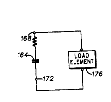
FIG. 6 is a partial circuit srh^mAtic partial block diagram of
the equivalent circuit of FIG. 5 connecte~l at nodes 168 and 172 thereof
1 0 across load elçment 176. When the electrical charge stored upon one
of the plate m~ nhers of capacitor 164 is above a certain level,
~igrh~Arge of the gtored charge occurs, thereby generating a current
that may be utilized to power load elçm~nt, 176. A capacitive circuit,
~imilAr to the equivalent circuit of FIG. 5, when connPcte~l across a
1 5 load Plçment 176 as shown in FIG. 6, forms the capacitive power
supply to power thereby a load ~lem^nt, such as load elp~m~nt 176,
according to the teArhin~ of the present inVçntion-
~ ApAritor ~legi~nR are now known which are of high capacitivevalues and which are also of small physical ~limencions. In
20 particular, and according to the teArhin~ of the plefelled
çmho-limen~ of the present invention~ a capacitor formed of a
conductive, ceramic material, and separated by an aqueous
electrolyte of a desired ~ielectric value forms a capacitor of a high
capacitance. Such capacitor ~lesignR have been ~lisrlose~l, for
25 e~mple in an article entitled, "Improved Pulse Power Sources With
High-Energy Density CApAritor" by H. Lee, G.L. Bullard, G.C.
MA~O~1, and K. Kern in the IEEE TrAnR~rtion~ on MAgnetics v.25 n. 1,
J_nuary 1989, pp. 324-330, and an article entitled "Operating
Principles of the IJltracapacitor" by G.R. Bullard, H.B. Sierra-
30 Alcazar, H.K. Lee, and J.J. Morris in the IEEE TrAn~ctions onMAgnetics, v. 25, n.1, January, 1989, pp.102-106. Additionally,
CAn~liAn Patent No. 1,196,683 by Dwight R. Craig, issued on
November 12, 1985, discloses ~imilAr capacitor ~iesign~ and methods
for m~lring such capacitor ~e~ign~.
-12- 2070178
A capacitor comprised of such a conductive, ceramic material
can form a capacitor of a capacitance of a~ o~;mAtoly 6000 farad8
having a potential difference across the oPpo~ine sides thereof of
approximately 1.2 volts. A capacitor having similAr properties may
5 also be constructed wherein the dielectric material is comprised of a
nonaqueous material or a solid state material.
For instonr~ FIG. 7A illustrates a plurality of plates 182 and
186 wherein plates 182 are interconnectstl by leads 190 and plates 186
are interconnPcts~l by leads 192. A pluralit,y of capacitive elemen
ea~h formed of a plate-pair 182-186 are cQnnecte~l in a parallel
cor~nection by leads 190 and 192, respectively, thereby. (It is noted that
any two adjacent plates 182-186 can form a plat,e-pair 182-186.) When
the plurality of plates 182 are interconn~ct~-l by leads 190, the
plurality of plates 182 together form a single surface comprised of
surface portions formed of individual ones of the plates 182.
~imil~rly, when the plurality of plates 186 are interconnect~l by leads
192, the plurality of plates 186 together form a single surface
c~ ,l;sed of surface portions formed of individual ones of the plates
186. Such a configuration having twenty-five, or fewer, capacitive
element~ (i.e., a total of fifty, or fewer, plates 182 and 186) wherein
each plate 182 and 186 is of a size of forty square cçntimpters (area) in
lengthwise and widthwise iimencions~ and five _ils or less in
height, forms an equivalent capacitive circuit having a capacitive
value of a~l,lo~;...Ato!y 6000 farads and a potent;Al dLfference of 1.2
25 volts across o~ o~ g sides of the circuit. It is to be noted that greater
or fewer plate-pairs 182-186 may be llt~li7e~ to form circuits of other
characteristics as desired. As a single, a~ o~l;ately-sized, plate-
pair 182-186 may form a capacitive circuit of desired characteristics
(including a circuit of 6000 farads and a potential difference of 1.2
30 volts), the capacitive elem~Pnt~ and illustrations thereof, which follow
will be described with reference to a single plate-pair. It is to be
understood, however, that such a capacitive element may Art~lAlly be
comprised of a plurality of plate-pair comhin~tion~ as shown in FIG.
7A.
2070178
- 13-
Connection of eight of ~uch capacitors in a series connection,
gimil~lr to the connection of the circuit s~hem~ic of FIGs. 3 and 4,
and represented by the equivalent circuit of FIG. 5, increases the
current generative ability of the resultant circuit formed therefrom.
5 A potential difference scross opposite ends thereof (as in~lic~te~l in
FIG. 5, across nodes 168 and 172) of approYim~tely 9.6 volts may be
obt~ine-l from such series connection of eight capacitors.
The equivalent capacitance of eight of such 6000 farad
capa~itors generates a current of a level, during ~ rge of the
- 10 capacitors, great enough to power a radiotelephone, such as the
Motorola MICRO T.A.C. 950 PT Personal Cellular Telephone ~,vbich
is commercially available, and which has a nomin~l input voltage of
6.3 volts and an input voltage operating range bet~veen 8.5 volts and
5.2 volts.
1 5 FIG. 7B is a cut-away, schem~tic view of a portion of sucb a
capacitive power supply, rerel 1 ed to generally in tbe Figure by
,bfele.lce numeral 200. Capacitive power supply 200 includes
housing 204 which 8U~Ol lively bouses eight capacitors 208, 212, 216,
220, 224, 228, 232 and 236. (It is again noted that capac~to~ 208-236
may ~ctll~lly be co~l;sed of a plurality of plates sucb as shown in
~TG.7A). Each capacitor 208-236 is of substantially simil~r
~limen~iong and construction, namely, each capacitor is co~ l;sed of
a ceramic, conductive material to provide a relatively thin power
source with a nominal voltage of 1.2 volts, and low, intrinsic, series
resist~nce. Separating opposing sides of each capacitor 208-236 is an
aqueous electrolyte, indicated by material 240 contained within the
int~ernal chamber formed of supportive housing 204. Gasket-like
memherg 242 are further illustrated for ret~ining the electrolyte
material 240 in position to prevent bridging (i.e., short-circuiting)
therebetween.
The e~ploded view of FIG. 7C~ illustrate~ a portion of a surface
of one plate of one capacitor 208-236. As illustrated, the surface is
rough, uneven, and sponge-like in appearance. The surface iB
~ctll~lly porous, and numerous pores 244 are indicated in the Eigure.
-14- 2070178
Such irregular surface increases the surface area formed upon the
plates of each of the capacitors 208-236; increases in the actual
surface area of each plate, increases the capacitance of the capacitors
208-236 formed the~eî~ ,l, and is partly r~eFoncible for the high-
capacitive quality of the reslllt~nt capacitor. While not shown in the
Figure, capacitors 208-236 are cQ~necte~l in a series cQnnectior~ by a
c~n~ll)rtive material. Capacitive power supply 200 of FIG. 7B is
ap~io"imately two inches in h?iEh~
Turning now to the block diagram of FIG. 8, a radiotelephone,
1 0 lefelled to generally by r~fel~Dnce nllmeral 260, constructed r~colding
to the te~rhir~ of the present invPnt;~ n, is illustrated.
Re liotelepl ~ne 260 is anrlose~l by block 176, shown in hatch, which
COlleS~JO~ to load elçmçnt 176 of FIG. 6. Suitable connection of
radiotelephone 260 to nodes 168 and 172 of the equivalent circuit of the
1 5 capacitive power supply perInits powering of the radiotelephone 260
thereby. The actual C~lC~Utl,~ embodying the filnr1;on~l blocks of
. ~iotelerhn~e 260 may be lli~o~e~l upon one or more circuit boards
and housed wit_in a couv ~.t;nnol radiotelephone housing. A
transmitted signal transmitted by, for eY~mrls, a base st~t;on of a
cellular, communication system, transmits a signal to Antenn~ 264.
~ntennq 264 gupplies the leceive signal on 268 to preselector/filter
272. Preselector/filter 272 is l,~efelably a very wi~leb~ntl filter having a
b~ebQntl to pass all of the freql~çn~ie~ within a band of interest.
Filter 272 ~;~ualstes a filtered signal on line 276 which is sl~pplie~l to
miser 280. Miser 280 addition~ly ~ece;ves an osrill~t;ng signal on
line 282 from an os~ tQr (not shown) which preferably forms a
portion of a o~u~ n~l phase locked loop. Miser 280 generates a
down coùvel led signal (commorlly referred to as a first interme-liAte
frequency ~ignDl) on line 284 which is supplied to filter 288. Filter 288
is, preferably, a monolithic crystal wi~bAn-l filter, and ig cQmmonly
referred to as the first interme-liAte frequency, i.e., IF filter.
Filter 288 generates a filtered signal on line 292 which is
supplied to ~mrlifier 296. ~mrlifier 296 Amplifies the signal supplied
thereto on line 292 and generates an ~mrlified signal on line 300.
-15- 2Q70178
Line 300 is coupled to an input to mixer 304 which al~o receives an
input on line 306 from an os~ll~tor, not shown, (which also
preferably comprises a portion of a convçntion~l phase locked loop).
Mixer 304 generates a mixed signal on line 308 which is supplied to
filter 312. Filter 312 forms a p~sb~nt1 of a bandwidth per_itting
p~ge of a desired signal on line 316. Line 316 is coupled to an input
Of ~mplifier/limiter 320 which generates a voltage limited signal on
line 324 which is supplied to ~l~m~~ t~r 328. Dçmo~ t~r 328
generates an output signal on line 332.
The block diagram of FIG. 8 further illustrates a transmit
portion of radiotelephone 260 comprising microphone 350, modulator
354, mixer circuit 360 and filter 366, the output of which is coupled to
Antenn~ 264.
It is to be noted that the l c~ive portion, i.e., the top portion of
1 5 the block diagram of FIG. 8, also describes a r~cei~er~ such as a
radio-pager, which may simil~rly be powe~ed by the capacitive power
supply of the present invention.
Turning now to the partial circuit srhçm~tic~ partial block
diagram of FIG. 9, the capacitive power supply, lepresrnt~tive by the
equivalent circuit of FIG. 5 is positioned to power load elçmPnt 176.
Positioned between the capacitive power ~upply and the load elçm~nt
176 is switching power supply 400. Switching power supplies are well
known per se in the art and filnctjon to generate a con~t~nt voltage
output respo~ ~ive to applir~tio~ of a wide range of voltages across an
input thereof. An e~mple of one such switching power supply is
M~ im Integrated Products Model No. MAX631 which co~ ises a
CMOS Fised~Adjustable Output Step-Up Switching Regulator.
Without switching power supply 400, and when the capacitive
power supply is coupled across a load elemçnt 176 as illustrated in
FIG. 6, the charge stored upon one of the plates of the capacitor 164 is
chD~rged as long as the potqnti~l difference formed across the
plates of capacitor 164 is above a pre-determine-l, minimum value.
Inclusion of the switching power supply as illustrated in FIG. 9,
2Q70178
- 16-
pe~nits ~lisch~rge of the stored charge of capacitor 164 bene~th this
pre-determined value.
FIG. 9 further illustrates line 402 c~nnsrting an enable input of
switching power supply 400 and load elemPnt 176. The enable input
5 _ay be lltili7e-1 to cau~e operation of switching power supply 400 only
when load alpmpnt 176 is connpcte l thereto. Alternately, five volt
etector 406 i8 alBo illuBtrated in FIG. 9 and cor necte-l acrQss load
element 176 by lines 407 and 408, shown in hatch, in the Figure may
be used to generate the ensble input 402 when the voltage acrQss load
10 çl~m~t, 176 falls hqne~th Sve volts. Inputs to swit~hing power supply
400 may cau~e o~,e, a~ion of supply 400 only when the voltage across
load elamp-nt 176 is below five volts, to çyte~l thereby, the opelaLional
period of 1~~ g of the load elPmpnt 176 by r~pA~tor 164.
FIGs. 10A and 10B are gr~phic~l reprçsant~t;on~ wherein
1 5 ordinate ases 410 are scaled in terms of volts, and ~bs~ia~A ases 420
are sc~led in terms of seron~l~. Line segm~nt 430 of FIG. 10A is
represent~t;ve of the voltage taken at the output side of switching
power supply 400, and as illustrated, is of a c~n~'~nt voltage. Curve
440 plotted in FIG. 10B is represPnt~t;ve of the voltage applied to the
input of ~witching power supply 400 which, for eY~mple, is nominally
6.3 volts for the radiotelephone 260 of FIG. 8, and which, in the
t,.~felled çmho~lim^-t~ may vary between ap~lo~ tely 1.2 volts and
8.5 volts. Over time, as the rem~ining charge stored by c~pacitcr 164
decreases, the corre~pon-ling voltage across capacitor 164, which is
s~lpplie~l to switching power supply 400, decreases. The inclusion of
switching power supply 400 permits powering of load elçment 176 by
the capacitive power supply for an eYt~n~le~l period of time. Switching
power supply may be disposed with the capacitive power supply and
housed within or at the housing of the power supply, such as housing
204 of FIG. 7B, or, alternately, ~witcLing power supply 400 may be
poge~l within load elçm^~ t 176.
The capacitive power supply of the present invention may be
advantageously ~lt;li7e-1 to power any electrical device such as a
portable radiotelephone, as the capacitive power supply is of small
-17- 20701 78
~iim^ngjQn8 may be charged at a very high rate, and i~ of an
llnlimitg~l life. Additionally, the capacitive power gupply may be
perm~n~ntly ~ffi-e-l to the load elçmçnt 176, as the unli_ited
recharging ability of the power supply does not require that a non-
5 perm~nent power supply, such a~ a conventional electrochemicabat~ery, be intennittently removed and repl~e~l
While the present invention has been described in co~nection
with the ~.efelled çmhodimpnt shown in the various figures, it is to
be understood that other ~imil~r çmho~limpnta _ay be u~ed or
10 m~lific~tions and r1tlitisns may be made to the descrihed
emho~liment~ for pe,rulming the same function of the present
invention without deviating therefrom. Therefol~, the present
invention ~hould not be limited to any single çmho~liment~ but rather
construed in breadth and ~cope in accordance with the recitation of
15 the appen~le-l cls~im~
What is rl~ime~l is: