Note: Descriptions are shown in the official language in which they were submitted.
~~~~~2~~.
1
OPT7CC~I. TI~,FFIC FItEEMPTICCN DETECTQR
BP.CKGROUND OF THE INVENTION
This invention relates to a system that allows emergency
vehicles to remotely control traffic signals, and more
specifically, a detector for use in such a system, wherein the
detector receives pulses of light from an approaching
emergency vehicle and transmits a signal representative of the
distance of the approaching vehicle to a phase selector, which
can issue a preemption request to a traffic signal controller.
Traffic signals have long been used to regulate the flow
of traffic at intersections. Generally, traffic signals have
relied on timers or vehicle sensors to determine when to
change traffic signal lights, thereby signaling alternating
directions of traffic to stop, and others to proceed.
Emergency vehicles, such as police cars, fire trucks and
ambulances, generally have the right to cross an intersection
against a traffic signal. Emergency vehicles have typically
depended on horns, sirens and flashing lights to alert other
drivers approaching the intersection that an emergency vehicle
intends to cross the intersection. However, due to hearing
impairment, air conditioning, audio systems and other
distractions, often the driver of a vehicle approaching an
intersection will not be aware of a warning being emitted by
an approaching emergency vehicle. This can create a dangerous
situation when an emergency vehicle seeks to cross an
intersection against a traffic signal arid the driver of
another vehicle approaching the intersection is ndt aware of
the warning being emitted by the emergency vehicle.
This problem was first successfully addressed in 'U. S.
Patent 3,550,078 (Long), which is assigned to the same
assignee as the present application. The Long patent
discloses an emergency vehicle with a stroboscopic light, a
plurality of photocells mounted along an intersection with
each photocell looking down an approach to the intersection,
a plurality of amplifiers which produce a signal
representative of the distance of the approaching emergency
vehicle, and a phase selector which processes the signal from
the amplifiers and can issue a request 'to a traffic signal
controller to preempt a normal traffic signal sequence to give
priority to the approaching emergency vehicle.
The Long patent discloses that as an emergency vehicle
approaches an intersection, it emits a series of light pulses
at a predetermined rate, such as 10 pulses per second, and
with each pulse having a duration of several microseconds.
A photocell, which is part of a detector channel, receives the
light pulses emitted by the approaching emergency vehicle.
An output of the detector channel is processed by the phase
selector, which then issues a request to a traffic signal
controller to change to green the traffic signal light that
controls the emergency vehicle's approach to the intersection.
zn the Long patent, each detector channel is comprised
of two photocells in parallel with an inductor. The
photocells also act as capacitors, so that the photocells and
the inductor form an LC resonant circuit. The resonant
circuit is tuned to oscillate at a predetermined frequency,
such as 6 KHz. The capacitance of the photocells and the
inductance of the inductor determine the frequency of
oscillation.
The inductor also acts as a DC short. Without the
inductor, a constant or slowly changing light source, such as
the sun or an approaching car headlight, would saturate the
photocells and render them ineffective. Therefore, the
inductor also acts to make the resonant circuit respond only
to quickly changing inputs.
When a photocell is presented with a pulse of light, the
resonant circuit produces a decaying sinusoid signal. The
signal is amplified and sent to the phase selector. By
measuring the magnitude of the decaying sinusoid signal, the
phase selector can determine the distance of the approaching
emergency vehicle.
Because the system taught by Long is dependent upon the
capacitance of the photocells and the inductance of the
inductor to produce the predetermined oscillation frequency,
each detector channel must always have two photocells. In a
typical intersection, there are four approaches. For example,
one street may approach an intersection from the east and west
and another may approach the intersection from the north and
south. In one embodiment, the two photocells in a detector
channel can be aimed in opposite directions, for example, one
aimed north and the other aimed south. Another detector
channel is used for the other street, with ane photocell aimed
east and the other aimed west. If an emergency vehicle
approaches, say from the south, the photocell that is pointed
south will activate the north-south detector channel. The
detector channel output signal will be processed by 'the phase
selector which will then issue a request to the traffic signal
controller to change the traffic signal lights to green in the
north and south direction and to red in the east and west
direction. The traffic signal lights are now set such that
the emergency vehicle can proceed through the intersection and
cross traffic will be required to stop.
In another embodiment, a typical four approach
intersection will use faur detector channels, with each
detector channel having its two photocells pointed in
approximately the same direction. In this embodiment, when
an approaching emergency vehicle is detected, the traffic
signal lights on three of the approaches will change to red.
The traffic signal lights controlling the emergency vehicle's
approach will change to green.
This embodiment requires four more photocells than are
physically needed to detect all approaches because the
detector circuit disclosed by Long must have two photocells
per detector channel to create the capacitance required for
the resonant circuit to oscillate at the predetermined
frequency. Long does nat disclose a circuit or method that
can have a variable number of photocells per detector channel.
The resonant circuit disclosed by Long creates another
problem; the inductor acts as an antenna and induces noise
into the circuit. The detector circuit requires extensive
shielding to minimize noise.
4
U.S. Patent 4,704,6.0 (Smith et al) also discloses an
emergency vehicle traffic control system. The Smith et al
patent discloses an emergency vehicle (chat transmits infrared
energy to a receiver mounted near an intersection. The
infrared energy transmitted by the emergency vehicle
preferably has a wavelength centered at approximately 0.950
micrometers and is modulated with a 40 KHz carrier.
The infrared receiver of Smith et al is comprised of a
photovoltaic detector in parallel with a tunable inductor.
The tunable inductor is adjusted to allow only signals
modulated with a 40 I~Hz carrier to be detected by the
amplifier/demodulator circuit. The tuned photovoltaic
detector/inductor circuit effectively eliminates LSO signals
from ~aackground solar radiation.
The detector circuit disclosed by Smith et al suffers
from the same problems as the detector circuit disclosed by
Kong; it is impossible to change the number of photocells per
detector channel without having to retune a resonant circuit
to maintain a predetermined frequency. Also, the inductor
disclosed by Smith et al, like the inductor disclosed by bong,
is likely to act as an antenna and therefore introduce radio
frequency noise into the detector circuit.
SUT~IMARY OF THE INVENTION
This invention provides an optical traffic preemption
detector assembly that detects pulses of light emitted by an
approaching emergency vehicle and provides an output signal
which is processed by a phase selector. The phase selector
can request a traffic signal controller to preempt a normal
traffic signal sequence to give priority to the emergency
vehicle.
The detector assembly is mounted in proximity to an
intersection and can have multiple detector channels. A
detector channel can have multiple photocells.
A detector housing includes a base, at least one detector
turret and a cap. Each detector turret can include a detector
circuit. A master detector circuit includes a circuit board,
a photocell module, a lens placed over the photocell module,
i
CA 02070251 2002-06-04
60557-4267
a summing circuit for summing an output from an auxiliary
detector circuit and circuitry to produce an output signal
capable of being received by a phase detector not in
proximity with the detector assembly. An auxiliary detector
5 circuit includes a circuit board, a photocell module and a
lens placed over the photocell module.
One aspect of the invention relates to a detector
assembly for receiving pulses of light from an emergency
vehicle and sending an output signal to a remote phase
selector. The detector assembly includes a detector housing
capable of being installed near a traffic intersection. The
detector housing includes a base for attaching to a support
structure. At least one detector turret is rotatably
coupled to the base for allowing a photocell to be aimed in
a direction. The detector housing also includes a cap
coupled to the detector turret for covering an end of the
detector housing. The detector assembly also includes a
detector circuit positioned in at least one of the detector
turret. The detector circuit includes a circuit board means
for providing conduction paths for components. Photocell
means are coupled to the circuit board means for providing
an electrical signal that varies with an intensity of light
striking the photocell means. Lens means are positioned
over the photocell means for intensifying and focusing light
striking the photocell means. Also, output means are
coupled to the photocell means for processing the electrical
signal produced by the photocell means into the output
signal capable of being received by a phase selector not in
proximity to the detector assembly.
CA 02070251 2002-06-04
60557-42&7
5a
BRIEF DESCRIPTION OF THE DRAWINGS
Figure 1 is a perspective view of a traffic
intersection which employs the detector assembly of the
present invention.
Figure 2 is an exploded view of one of the
detector assemblies of Figure 1.
Figure 3A is a side view of an assembled detector
assembly of Figure 2.
Figure 3B is a top view of the assembled detector
ZO assembly shown in Figure 3A.
Figure 4A is a side view of a master circuit
board, which is part of the detector assembly of Figure 2.
Figure 4B is a front view of a photocell side of
the master circuit board shown in Figure 4A.
Figure 5A is a front view of a component side of
the master circuit board of Figure 4A.
Figure 5B is a front view of a component side of
an auxiliary circuit board used in the detector assembly of
Figure 2.
Figure 6 is a block diagram of the circuitry
contained on the master circuit board and the auxiliary
circuit board of the detector assembly of Figure 2.
Figure 7 is a detailed circuit diagram of the
master circuit board of Figure 6.
I
CA 02070251 2002-06-04
60557-4267
5b
Figures 8A-8E are graphs of the waveforms present
at various stages in the circuitry of master circuit board
of Figure 7.
DETAILED DESCRIPTION OF THE PREFERRED EMBODIMENTS
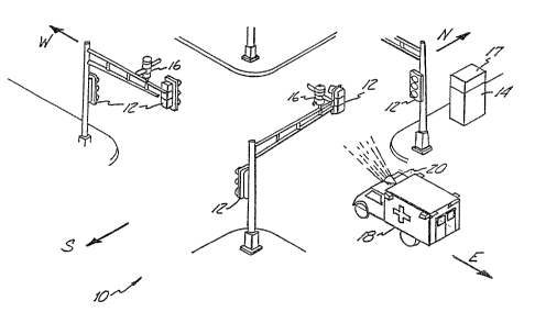
Figure 1 is an illustration of a typical
intersection 10 with traffic signal lights 12. Traffic
signal controller 14 sequences traffic signal lights 12 to
allow traffic to proceed alternately through the
intersection. Detector assemblies 16
are mounted to detect pulses of light emitted by emergency
vehicles approaching intersection 10. Detector assemblies 15
communicate with phase selector 17, which is typically located
in the same cabinet as traffic controller 14.
In Figure 1, emergency vehicle 18 is approaching
intersection 10. It is likely that the traffic light 12
controlling approaching emergency vehicle 18 will be red as
emergency vehicle 18 approaches the intersection.
Mounted on emergency vehicle 18 is optical transmitter
20, which transmits pulses of light to detector assembly 16.
Optical transmitter 20 emits pulses of light at a
predetermined interval, such as 10 to 25 pulses per second.
Each pulse of light has a duration of several microseconds.
Detector assembly 16 receives these pulses of light and sends
an output signal to phase selector 17. Phase selector 17
processes the output signal from detector assembly 16 and
issues a request to traffic signal controller 14 ~:o preempt
a normal traffic signal sequence. In Figure 1, if optical
transmitter 20 on emergency vehicle 18 emits pulses of light
at the predetermined interval, with each pulse having
sufficient intensity and fast enough rise time, phase selector
1? will request traffic signal controller 14 to cause the
traffic signal lights 12 controlling the northbound and
southbound directions to become red and the traffic signal
lights controlling the westbound direction to become green.
Ln one embodiment, phase selector 17 requests that only
the traffic signal lights that control an approaching
emergency vehicle to become green, and the traffic signal
lights controlling the other three approaches become red. In
another embodiment, phase selectar 17 requests that the
traffic signal lights controlling the street on which the
emergency vehicle is approaching to become green in both
directions. The traffic signal lights controlling the street
perpendicular to~the emergency vehicle°s approach are changed
to red. The difference between these two embodiments is that
the former embodiment requires four channels and the latter
embodiment requires two channels. If two channels are
employed, two photo detectors pointing in opposite directions
activate the same channel. If four channels are employed,
each photocell activates its own channel.
Figure 2 is an exploded view of detector assembly 16 of
Figure 1. Detector assembly 16 includes base unit 20,
detector turrets 22A and 22B and cap 26.
Base unit 20 is a cylindrical shaped housing having
rectangular proaection 28 and circular opening 30.
Rectangular opening 32 is located on rectangular projectian
28. When detector assembly 16 is assembled, cover 34 is
fastened over rectangular opening 32 by screws 36. When cover
34 is removed, cover 34 retains screws 36 and is kept in
proximity to base unit 20 by tether 37. Terminal strip 38 is
connected to wires from cables 40 and 42. Cable 40 enters
base unit 20 through cable entry port 44. Near circular
opening 30 are threaded center shaft hole 46 and stop plate
48. Span wire clamp 50 has threaded portion 52, which can be
screwed into threaded hole 80 (shown in Figure 3A). When
detector assembly 16 is assembled, gasket 54A is positioned
between detector turret 22A and base unit 20.
Base unit 20 serves as a point of attachment for mounting
detector assembly 16 near an intersection. Detector assembly
16 can be installed in one of two ways; upright, with base
unit 20 at the bottom of detector assembly 16, or inverted,
with base unit 20 at the top of detector assembly 16. Weep
hole 56 can be opened by knocking out a plug if detector
assembly 16 is installed in the upright position. Weep hole
56 allows accumulated moisture to dissipate from the interior
of detector assembly 16.
~f detector assembly 16 is installed on a mesa arm of a
traffic control signal, detector 16 can be installed in either
the upright or the Inverted position. If the mast arm is
hollow and can carry wiring, cable 40 can enter detector
assembly 16 through the same threaded hole 80 (shaven in Figure
3A) that Is used to mount detector assembly 16 to the mast
arm. lHowever, if the mast arm can not carry wiring, or It is
not convenient to route cable 40 through threaded hole 80,
~~~~~~ya~~
cable 40 can enter detector assembly ~.6 through cable entry
port 44. _
If detector assembly Z6 is mounted to a span wire,
detector assembly 16 is typically mounted in the inverted
position. Span wire clamp 50 is clamped to the span wire, and
threaded portion 52 of clamp 50 is screwed into threaded hole
80 of base unit 20. Detector assembly 16 is suspended in the
inverted position from the span wire. In 'this type of
installation, cable 40 must enter detector assembly 16 though
cable entry port 44.
When detector assembly 16 is assembled, terminal strip
38 is positioned inside an interior of base unit 20. Terminal
strip 38 connects cable 40, which leads to phase selector ~.7
of Figure 1, to cable 42, which leads to detector turret 22A.
One cable 42 is required for each detector channel, In the
embodiment shown in Figure 2 , there are two photocells coupled
to one detector channel. Therefore, only one cable 42 is
required. However, in other embodiments detector assembly 16
can include more than one channel, and therefore there would
be more than one cable 42 having wires connected to terminal
strip 38.
Circular opening 30 rotatably supports gasket 54A and
detector turret 22A. Stop plate 48 contacts a stop plate in
detector turret 22A to prevent detector turret 22A form
rotating more than 360 degrees with respect to base unit 20.
Threaded center shaft hole 46 is provided to receive a
threaded shaft, which holds detector assembly 16 together.
Detector turret 22A includes tube 58A, which has an
opening covered by window 60A. When detector assembly 16 is
assembled, master circu9.t board 62 is positioned within
detector turret 22A, with integrally formed lens and lens tube
64A coupled to master board 62 and extending into tube 58A.
Tntegrally formed lens and lens tube 64A is positioned in
front of photocell 65A. Cable 42 connects master circuit
board 62 with terminal strip 38. Cable 66 connects circuit
baard 62 with circuitry in detectar turret 22B. Detector
turret 22A alsa has stop plate 68A and a stop plate beneath
~~'~~~~.
tube 58A (not shown in Figure 1).
Tube 58A provides a visual indication of the direction
in which integrally formed lens and lens tube 64A is aimed.
This is helpful to installers and maintainers of detector
assembly 16 because they can determine from street level the
direction a detector turret is aimed. Window 60A is provided
to prevent spiders and other insects or small animals from
entering detector assembly Z6 and creating obstructions (such
as spider webs). It also shields detector assembly 16 from
rain, snow and other elements.
Integrally formed lens and lens tube 64A is coupled to
master circuit board 62 and directs light entering tube 58A
to photocell 65A. The lens in integrally formed lens and lens
tube 64A is a wide aperture lens that intensifies the light
striking photocell 65A and also selects a f field of view of
approximately eight degrees.
Cable 42 connects master circuit board 62 through
terminal strip 38 and cable 40 to phase selector 17 in Figure
1. Cable 42 provides a power supply voltage to master circuit
board 62 and returns a detector channel output signal from
master circuit board 62 to phase selector 17. Cable 66
connects master circuit board 62 to an auxiliary circuit board
in detector turret 228. Gasket 54B separates detector turret
22A from detector turret 22B and seals tine rotatable interface
between the two detector turrets from moisture, dirt and other
elements.
Detector turret 228 is similar to detector turret 22A.
Detector turret 22B has tube 588, window 60B, integrally
formed lens and lens tube 64B, photocell 65B (shown in Figure
6), stop plate 688 and a stop pate beneath tube 58B (not seen
in Figure 2), I~Iowever, unlike detector turret 22A, detector
turret 22B has auxiliary circuit board 70.
Auxiliary circuit board 70 has a small subset of the
circuitry on master circuit board 62. When photocell 65B
receives a pulse of light, a signal is sent via cable 66 to
master circuit board 62. Master board 62 processes the signal
and sends it to phase selector 17 in Figure 1. In the
~~"~~~ ~:~.
embodiment shown in Figure 2, phase selector 1'7 cannot
determine whether the output signal of detector assembly 16
originated from photocell 65B on auxiliary circuit board 70
or photocell 65A on master circuit board 62.
5 When detector assembly 16 is assembled, gasket 54C seals
the interface between detector turret 22B and cap 26 from
moisture, dirt and other elements. Like weep hole 56 in base
unit 20, weep hole 72 in cap 26 can be opened by knocking out
a plug if detector assembly 16 is to be installed in an
10 inverted position.
Center shaft 74 extends through O-ring ?6, hole 78 in cap
26, detector turrets 22B amd 22A and associated gaskets, to
threaded center shaft hole 46 in base unit 20. After
installing detector assembly 16 and aiming the detector
turrets in the proper direction, center shaft 74 is tightened
to lock detector turrets 22A and 22B in place and hold
detector assembly 16 together.
Base unit 20, detector turrets 22A and 22B and cap 26 are
comprised of molded polycarbonate plastic. The polycarbonate
plastic must be opaque to electromagnetic radiation in the
visible and infra-red spectra to insure proper operation of
the detector circuitry. Such a polycarbonate plastic is
manufactured by Mobay. The Mobay product number for this
material is M39L1510.
Figure 3A shows an assembled detector assembly 16 of
Figure 2. In addition to the elements shown in Figure 2,
Figure 3A shows threaded hole 80, for mounting detector
assembly 16 to a traffic signal mast arm or span wire clamp
50 of Figure 2.
Tubes 58A and 58B have ends which are cut at an angle.
Detector assembly 16 is always installed with the tubes
posi~tianed such that the shorter side of each tube 58A and 58B
is closer to the ground. Figure 3A shows detector assembly
16 assembled for installation in the upright position. Tf
detector assembly 16 is to be mounted in the inverted
position, detector turrets 22A and 2218 would have 'to be
inverted so that when detector assembly 16 is inverted, the
11
shorter side of each tube is eloser to the ground.
Figure 38 is a top view of the detector assembly 16 shown
in Figure 3A. Figure 3B illustrates, by having tubes 58A and
58B separated by an angle of less than 180 degrees, how tubes
58A and 58B can be adjusted to adapt to the topography of the
intersection where detector assembly 16 will be installed.
Figure 4A is a side view of master circuit board 62 of
Figure 2. Master circuit board 62 has photocell side 84,
which includes photocell 65A and integrally formed lens and
l0 lens tube 64A, and component side 86, which includes the
components that form the detector circuitry.
Integrally formed lens and lens tube 64A is attached to
master circuit board 62 by two retainment tabs 82 that
protrude through master circuit board 62. Integra7.ly formed
lens and lens tube 64A is preferably formed of polycarbonate
plastic by an injection molding process. This material and
process provides cost advantages, excellent resistance to high
temperatures, and superior alignment with respect to photocell
65A. The lens has an aperture of approximately f 1.0, a
diameter of approximately 0.644 inches, a maximum thicleness
at its center of approximately 0.218 inches, and selects a
field of view of approximately 8 degrees.
Figure 4B is a front view of photocell side 84 of master
circuit board 62. Tn addition to the elements shown in Figure
4A, Figure 4B shows ground plane grid 90. Ground plane grid
90 helps prevent electrical noise emanating from component
side 86 from interfering with the operation of photocell 65A
on detector side 84 by shielding the two sides from each
other. Because many of the components on master circuit board
62 are surface mounted, the component terminals do not have
to protrude through the board. This further enhances the
shielding effect of ground plane grid 90.
photocell side 84 of master circuit board 62 is nearly
the same as a photocell side on auxiliary circuit board 70 of
Figure 2. Auxiliary circuit board 70 has photocell 658,
integrally formed lens and lens tube 64B and a ground plane
grid on a photocell side in an arrangement similar to that
~2 ~'~~ ~.~.
shown in Figure 4B, Although auxiliary circuit board 70 and
master circuit board 62 have photocell sides that are similar,
'their component sides are different.
Figure 5A shows component side 86 of master circuit board
62. Component side 86 is fully populated with the components
necessary to form a detector channel. Also shown in Figure
5A are retainment tabs 82, which couple integrally formed lens
and lens tube 64A of Figure 4A to mae~ter circuit board 62.
Figure 5B shows component side 92 of auxiliary circuit
board ?0. Component side 92 is only partially populated. The
only circuitry that component side 92 has is a filter formed
from a resistor and a capacitor, and a connector which
connects an auxiliary circuit board ?0 to a master circuit
board 62. Master circuit board 62 then performs signal
processing on a signal combined from signals originating from
photocell 65A on master circuit board 62 and photocell 65B on
auxiliary circuit board ?0.
Figure 6 is a block diagram of the circuitry included on
fully populated master circuit board 62 and partially
populated circuit board ?0 similar to those shown in detector
assembly 16 of Figure 2. The circuitry includes photocells
65A and 65B, rise time filters 96A arid 968, circuit node 9?,
current--to-voltage (I/V) converter 98, band pass filter 100,
output power amplifier 102 and detector channel output 104.
Photocells 65A and 65B receive pulses of light from an
emergency vehicle. Rise time filters 96A and 96B allow only
quickly changing signals caused by pulses of light to pass.
Rise time filters 96A and 968 are high pass filters tuned to
a specific frequency, such as 2 KHz.
Each rise time filter 96A and 96B produces an electrical
signal having a current that represents a pulse of light
received by a photocell. Circuit node 9? sums the currents
produced by rise time filters 96A and 96B. Although the
embadiment shown in Figure 6 only has two photocells, circuit
node 9? makes it possible to have additional photocells on the
same detector channel; an advancement over the prior art where
a resonant frequency had to be tuned based on the number of
13
photocells.
I/V converter 98 converts the current signal summed by
circuit node 97 into a voltage signal, which can be processed
more conveniently than a current signal. Band pass filter 100
isolates a decaying sinusoid signal from the spectrum of
frequencies present in the pulse signal generated by a
photocell and a rise time filter in response to a pulse of
light. Output power amplifier 102 amplifies the decaying
sinusoid signal isolated by band pass filter 100 and provides
detector channel output 104 to phase selector 17 of Figure 1.
For each pulse of light received by photocell 65A or 65B,
detector channel output 104 produces a number of square wave
pulses, wherein the number of square wave pulses varies with
the intensity of the light pulse received by the photocell.,
Figure 7 is a detailed circuit diagram showing an
embodiment of the circuitry included on master circuit board
62 and shown as a block diagram in Figure 6. In Figure 7,
master circuit board 62 has photocell 65A, rise time filter
96A, circuit node 97, T/V converter 98, band pass filter 100,
output power amplifier 102, detector channel output 104, power
supply 106, bias voltage supply 108 and connectors JP1 and
JP2.
Connector JP2 is a three pin plug that is connected to
terminal strip 38 by cable 42 in Figure 2. Connector JP2 is
only connected to a fully populated master circuit board 62
and supplies the board with a DC supply voltage .and ground
GND. Tn this embodiment, the DC supply voltage provided by
connector JP2 is approximately 26 volts. Connector JP2 also
connects detector channel output 104 to terminal strip 38,
which is also connected to phase selector 17 of F9.gure 1.
Power supply 106 converts a DC supply voltage coming from
connector JP2 into a regulated voltage V1. Power supply x.06
includes diodes D3 and D7, capacitors C9 and C10, regulator
U3 and an output.
T'he DC supply voltage from connector JP2 is connected to
an anode of diode D3. Capacitor C9 is a polarized capacitor
with a negative terminal connected to ground GND and a
:~ ~P
14
positive terminal connected to the cathode of diode D3.
Regulator U3 has input VI, output VO and ground terminal GD.
Ground terminal GD is connected to the ground GND. Input VI
is connected to the cathode of diode D3. Diode D7 has a
cathode connected to input VI of regulator U3 and an anode
connected to output VO of regulator U3. Polarized capacitor
C10 has a positive terminal connected to output VO of
regulator U3 and a negative terminal connected to ground GND.
Output VO of regulator U3 provides the output for power supply
106. The output of power supply 106 is supply voltage V1.
In this embodiment, V1 is 15 volts. Supply voltage V1 is
distributed throughout master circuit board 62, along with
ground potential GND from connector JP2.
Bias voltage supply 108 divides supply voltage V1,
producing bias voltage V2. In this embodiment, bias voltage
V2 is one half of supply voltage V1, or 7.5 volts. Bias
potential supply 108 includes resistors R11 and R12 and
capacitor C8. The output of bias voltage supply 208 is bias
voltage V2.
Resistors R11 and R12 form a voltage divider, with
resistor R22 connected between supply voltage V1l and bias
voltage V2 and resistor R11 connected between bias voltage V2
and ground GND. Bias voltage supply 108 also has polarized
capacitor C8, with a positive terminal connected to bias
voltage V2 and a negative terminal connected to ground GND.
Photocell 65A is comprised of photodiode D1. Photodiode
D1 operates in a photovoltaic mode and produces a low level
current signal when exposed to light. Photodiode D1 has an
anode that is connected to ground GND and a cathode that
serves as an output of photocell 65A. Photodiode D1 would
perform equally well in the circuit of Figure 7 if the cathode
is connected to ground GND and the anode serves as the output
of photocell 65A.
Photodiode D1. is a silicon PIN photocell with a
relatively small active area of approximately 0.~, inches by
0.09 inches. A relatively small active area is desirable
because it tends to minimize variations between photodiodes.
15
Photodiode D1 is mounted to a circuit board with the long axis
vertical to minimize the horizontal detection angle and
maximize the vertical detection angle.
Although photodiode D1 is used to receive pulses of light
from a stroboscopic light mounted on an emergency vehicle,
industry standards typically require that electrical
specifications be given for a photodiode illuminated with a
2800 degree K tungsten light. zncluded in the specifications
that Photadiode D1 must meet are the following. when
irradiated with 100 microwatts/cm2 of 2800 degrees K tungsten
light with photodiode D1 at 23 degrees C, photodiode D1 has
a forward open circuit voltage of at least 0.250 volts, and
a forward current into a 1000 ohm series resistance of at
least 1.2 microamps. when no light illuminates photodiode D1,
it has a reverse current that does not exceed 1.5 microamps
at 1.000 +/- 0,002 volts DC at 25 +/-- 3 degrees C. The
forward voltage drop of photodiode D1 must net exceed 2.0
volts with an applied 10 milliamp forward current.
Rise time filter 96A is a high pass filter that allows
only quickly changing signals to pass. Rise time filter 96A
includes resistor R1 and capacitor C1. Resistor R1 has one
terminal connected to ground GND and another terminal
connected to the output of photocell 65A. Capacitor C1, has
one terminal connected to the output of photocell 65A and
another terminal that serves as an output for rise time filter
96A.
The output of rise time filter 96A, is connected to T/V
converter 98. I/V converter 98 includes operational amplifier
(op amp) U1A, resistor R2 and an output. Op amp UlA is
3U powered by connections to supply voltage V1 and ground GND.
Op amp UlA has a noninverting input connected to bias voltage
V2 and an inverting input connected to the output of rise time
filter 96A. Resistor R2 is connected between 'the inverting
input of op amp UlA and an output of op amp UIA. The output
of op amp UlA is the output of I/V converter 98.
In the embodiment shown in Figure 7, band pass filter 100
is implemented as first band pass filter stage 110 and second
16
band pass filter stage 112. The two band pass filter stages
110 and 112 are of nearly identical construction, and a
detailed explanation of one applies to the other.
First band pass filter stage 110 lass resistors R3, R4 and
R5, capacitors C2 and C3, op amp U1B, common node 114, an
input and an output. The output of I/V converter 98 is
connected to a terminal of resistor R3. This terminal of
resistor R3 serves as the input to first band pass filter
stage 110. Another terminal of resistor R3 is connected to
common node 114. Also connected to common node 114 are a
terminal of resistor R4, a terminal of capacitor C2 and a
terminal of capacitor C3. Resistor R4 has a second terminal
connected to bias voltage V2, capacitor C3 has a secand
terminal connected to an output of op amp U1B and capacitor
C2 has a second terminal connected to an inverting input of
op amp U1B. Resistor R5 is connected between the inverting
input of op amp U1B and the output of op amp U1B. Op amp U1B
is powered by connections to supply voltage V1 and ground GND
and has a noninverting input connected to bias voltage supply
V2. The output of op amp U1B is also the output of first bared
pass filter stage 110, and is coupled to an input of second
bass pass filter stage 112.
As previously noted, second band pass filter stage 112
is of nearly identical construction to first band pass filter
stage 110. Becond band pass filter stage 112 has resistors
R6, R7 and R8, capacitors C4 and C5, op amp U2A, common node
116, an input and an output. The following components serve
equivalent functions in the two band pass filter stages:
resistor R3 and resistor R6, resistor R4 and resistor R7,
capacitor C2 and capacitor C4, capacitor C3 and capacitor C5,
resistor R5 and resistor R8, common node 114 and common node
116 and op amp U1B and op amp U2A.
The output of second band pass filter stage 112, which
is the output of op amp U2A, is coupled to output power
amplifier 102. Output power amplifier 102 includes resistors
R9 and R10, capacitor C%, diodes D4, D5 and D6, op amp U2B and
detector channel output 104.
17
The output of second band pass filter stage 112 connected
to a terminal of resistor R9. Another terminal of resistor
R9 is connected to an inverting input of op amp U2B. Op amp
U2B is powered by connections to supply voltage V1 and ground
GND and has a non--inverting input connected to bias voltage
V2. Resistor R10 is connected between the inverting input of
op amp U2B and an output of op amp U2B. Diode D4 has an anode
connected to the inverting input of op amp U2B and a cathode
connected to the output of op amp U2B. Diode D5 has an anode
connected to the output of op amp U2B and a cathode connected
to power supply voltage V1. Diode D6 has an anode connected
to ground GND and a cathode connected to the output of op amp
U2B. Together, diodes D5 and D6 provide surge protection and
insure that the output of output power amplifier 102 is a
signal that does not exceed the limits of supply voltage V1
and ground GND. Capacitor C7 is connected between the output
of op amp U2B and detector channel output 3.04. Capacitor C7
removes the DC voltage component from detector channel output
104.
In this embodiment, the circuit of Figure 7 is
constructed with the components listed in Table I.
Table I
Resistors
R3, R6, R9 4.32K Ohms
R1, R11, R12 7.50K Ohms
R2 40.2K Ohms
R4, R5, R?, R8, R10 143K Ohms
D~.Odes
D1 Photodiode
D3, D5, D6, D7 IN4002
D4 IN4148
Cauaaito~cs
C1 .O1 micro Farad
C2, C3, C4, C5 .0001 micro Farad
C? .1 micro Farad
C10 1 micro Farad
C8, C9 4.7 micro Farad
18
~~axat~,4aa Aynpl3fiexs
UIA, U1~, U2A, U2B MC 33078D
it~gulat~x
U3 LT~7 815
The operation of the circuit of Figure 7 will be
explained in detail with reference to Figures 8A-8F, which
represent waveforms present in various sections of the circuit
of Figure 7. Figures 8A-8E are exaggerated to better
illustrate the operation of the circuit of Figure 7, and
therefore, the scale and timing of Figures 8A~8E are not an
exact depiction of the actual waveforms.
Photodiode D1 of photocell 65A operates in a photovoltaic
mode. In this mode, photodiode D1 produces a small electrical
current that varies with the amount of light it receives.
Figure 8A is a graph showing a typical current signal coming
from photodiode D1 as an approaching emergency vehicle (as
shown in Figure 1) is emitting pulses of light to preempt the
normal sequence of traffic signal lights 12 of Figure 1.
As seen in Figure 8A, the signal from photodiode D1 has
a constant component (due to street lights, daylight and othex
constant sources), a slowly varying component (due to
approaching car headlights and other slowly varying sources)
and a quickly changing component (due to the pulses of light
emitted by an approaching emergency vehicle). The pulses of
light emitted by the approaching emergency vehicle are several
microseconds in duration and ar_e repeated at a predetermined
rate, such as 10 pulses per second.
The output of photocell 65A is presented to rise time
filter 9f>A. As seen in Figure 8B, rise time filter 65A
eliminates the constant and slowly varying campone:nts of the
signal emitted by pho~todiode D1 shown in Figure 8A.
An impartant advantage of this invention is 'that it
allows a variable number of photocells to be placed on the
same detector channel. At circuit node 97, the output of
another photocell and rise time filter connected to pin 3 of
connector JP1 can be summed with the output of photocell 65A
19
and rise time filter 96A.
The circuit of Figure 7 shows a fully populated master
circuit board 62. However, if a second photocell 65B is to
be added on the same channel, it is mounted on a partially
populated auxiliary circuit board 70 (as shown in Figures 2,
5B and 6). The only components from Figure 7 that are on an
auxiliary circuit board 70 are photocell 658, rise time filter
96B and four pin plug connector JP1. Cable 66 (shown in
Figure 2) connects connector JP1 on a master circuit board 62
to connector JP1 on an auxiliary circuit board 70. Node 97
sums the current signals produced by the pair of photocells
65A and 65B and rise time filters 96A and 96B.
The current output of at least one rise time filter 96A
or 96B is coupled to the input of Y/V converter 98. As seen
in Figure 8C, T/V converter 98 produces a series of valtage
pulses imposed on a constant voltage equal to bias voltage V2.
These voltage pulses are applied to band pass filter 100.
Band pass falter 100 is comprised of first band pass
filter stage 110 and second band pass filter stage 112. Each
band pass filter stage 110 and 112 has two poles plus a gain.
The combined effect of the two band pass filter stages 110 and
112 is to provide a greater roll-off from the center frequency
than would a single band pass filter stage. This provides
superior rejection of 60 Hz and 120 Hz signals.
Figure 8D is an illustration of the signal produced by
band pass filter 100. Band pass filter 100 receives the
voltage pulses shown in Figure 8C and isolates a decaying
sinusoid signal from the spectrum of frequencies contained in
a voltage pulse. In this embodiment, band pass filter 100 has
a center frequency of approximately 6.5 KHz.
'I~he decaying sinusoid signal produced by band pass filter
100 is applied to autput power amplifier 102. output power
amplifier 102 has diode D~, which shunts a portion of the
signal from band pass filter 100 that is below bias voltage
V2. Additionally, the combined effect of the gain stages of
first band pass filter stage 110, second band pass filter
stage 112 and output power amplifier 102 is to amplify the
a ~.
decaying sinusoid signal until it reaches the limits imposed
by supply voltage V1 and ground GND. Figure 8E shows the net
effect of retaining only the positive component of the signal
and amplifying the signal to the limits of the range of op amp
5 U2B.
Figure 8E also shows the signal that the circuit of
Figure 7 transmits to phase selector 1'7 of Figure 1. Figure
8E shows a series of pulse packets, with each pulse gacket
corresponding to a single pulse of light emitted from the
10 approaching emergency vehicle. As the emergency vehicle
approaches, the number of pulses per packet transmitted by the
circuit of Figure 7 will increase. Ira general, the amplitude
of the pulses will be equal to the maximum output of output
power amplifier 102. However, there may be one pulse at the
15 end of a decaying sinusoid signal of such a small magnitude
that it is not amplified to the maximum output of output power
amplifier 102, thereby producing a smaller pulse. Figure 8E
shows such a smaller pulse at the last pulse of each pulse
packet in Figure 8E.
20 Phase selector 17 of Figure 1 can determine the distance
of an approaching vehicle by taunting the number of pulses per
packet. With this information, phase selector 17 can request
traffic signal Controller 14 to preempt a normal traffic
control light sequence and signal cross traffic to stop and
the approaching emergency vehicle to proceed through the
intersection.
This invention has been developed for use as part of an
Opticom Priority Control System, manufactured by Minnesota
Mining and Manufacturing Company. The Opticom system is
similar to a system disclosed by Long irt U.S. Patent
3,550,078. The present invention provides a signal that is
compatible with previously installed Opticom systems.
Besides signal format Compatibility, this invention
provides an increase in range over priar Opticom detectors.
Prior Opticont detectors could not detect an approaching
emergency vehicle until it was within 1800 feet of the
detector. This invention provides an Opticom system with
21
greater range without having to replace the rest of the
system; only the detector assemblies need to be replaced.
This invention achieves greater range than priar Opticom
detectors by increasing the sensitivity and signal-to°noise
ratio of the detector channel. Several factors contribute to
these improvements. First, a lens is placed over the
photocell, intensifying the light received by the photocell
and reducing the area of the photocell (which reduces noise
generated by 'the photocell). Second, the inductor used in
prior art circuits has been removed. The inductor acted as
a large antenna and induced noise into the detector channel.
The inductor also required extensive shielding, adding cost
and complexity to a detector channel. And third, the
components are on a surface mounted board in proximity to the
photodiode, reducing the distance that an unamplified signal
has to travel before being amplified and thereby reducing the
ability of noise to be induced into the circuit. In prior
detectors, the detector circuitry was placed in the base of
the detector assembly, not close to the photocells.
Another advantage of this invention is increased
modularity. In prior detectors, each detector channel had to
have two photocells. If an approach to an intersection
required its own channel, both photocells where aimed in the
same direction. Additionally, prior detectors allowed only
one channel per detector assembly. Therefore each detector
assembly had two photocells and one channel.
This invention allows a variable number of detectors per
channel, and a variable number of channels per detector
assemb7.y. By replacing the resonant circuit, which depended
on having two photocells to provide the required capacitance,
with a rise time filter and a I/V converter, any number of
photocells can be connected to a channel. By putting the
circuitry associated with a detector channel on a single board
with the photocell, multiple detector channels can be placed
in the same assembly.
Although the present inventian has been described with
reference to preferred embodiments, workers skilled in the art
22
wild. recognize that changes may be made in form and detail
without departing from the spirit and scope of the invention.