Note: Descriptions are shown in the official language in which they were submitted.
2070700
S P E C I F I C A T I O N
TITLE
"METHOD AND CIRCUIT ARRANGEMENT FOR LIMITING AN OUTPUT SIGNAL"
BACKGROUND OF THE INVENTION
Fleld o~ the Invention
The present invention is directed to a method and circuit arrangement for limiting
an output signal which is derived from a pulse-duration-modulated signal via circuitry
having a demodulating effect.
Description o~ the Prior Art
A circuit specifically designed for use in battery-operated hearing aids for
minimizing power consumption is disclosed in German Patent 36 16 752. For this
purpose, demodulation of the pulse-duration-modulated control signal ensues in an output
stage (Class D amplifier~ operating in switched mode in combination with the low-pass
effect of the earphone of the hearing aid, which is already required. It is known to limit
the amplitude of the output signals (useful signals) in hearing aids using peak clipping
circuits in the output stage. Given a pulse-duration-modulated signal, the amplitude of the
output signal, however, is coded in the duration (width) of the individual pulses of the
control signal which is used to switch the output stage. The arnplitude of the useful signal
(base signal) coded in pulse duration therefore cannot be limited in the output stage using
conventional methods or circuit arrangements. It is possible to limit the power of the
output stage by means of a reduced operating voltage, or operating current, supplied to
the earphone. This approach, however, results in an undesirable reduction in the
amplification and power of the demodulated output signal. In order to avoid this
disadvantage, in practice the useful signal is lim~ited before reaching the output stage, in
a preselection stage, and the pulse-duration-modulation is produced with this already-
limited useful signal. An undesired spectral spread of the useful signal even before the
~, ~
207~7~0
pulse-duration modulator arises as a result of this approach, which leads to undesirably
hi~,.. reconvolution products (high distortions) tn the output signal.
SUMMARY OF THE INVENTION
It is an ob~ect of the present invention to provide a method and circuit arrangement
for limiting an output signal derived from a pulse-duration-modulated control s7gnal
through circuitry having a demodulating effect in which limitation of the oulput signal
(useful signal) is achieved without reducing the amplification gain and with low distorUon.
The above obJect is achieved in accordance with the principles of the present
invention in a method and circuit arrangernent wherein additional pulses for the limitation
are generated from the aggregate signal (base signal plus sampling signal), generation
of the aggregate signal being already required for the pulse duration modulation. These
additional pulses arise only when a threshold voltage, which is preferably adlustable, is
upwardly transgressed by the aggregate signal. The additional pulses are Inserted into
the pulse-duration-modulated control signal as additional modulation. The additional
pulses in the control signal effect a limitation in the amplitude of the demodulated output
slgnal ~useful signal) only after ampllfication has already occurred, and given
demodulation of the control signal. A limitation in ihe amplitude of the ampli~led output
$ ~ L siynal is thus achieved without reducing the gain (i.o.; without a powor roduotion), for
a. ,~. example in a switched output stage, and with only slight distortion.
30,'t.9r
DESCRIPTION OF THE DRAWINGS
Figure 1 is an illustration of a base signal (useful signal) and a sampling signal of
the type used in the method and apparatus in accordance with the principles of the
present invention.
Figure 2 is an illustration of various signals and pulses generated in accordance
with the principles of the present invention In the method and apparatus disclosed herein.
-2-
~, .
.
Figure 3 is a block circuit diagram of a circuit arran~ement constructed 7n
ae ,rdance with the principles of the prssent invention, practicing the method shown in
Figure 2.
Figure 4 is a btock circuit diagram of a further embodiment of a circuit arrangement
constructed in accordance with the principles of the present invention.
Figure 5 is a block circult diagram of the circuit arrangement of Figur~ 4 in
combination with a hearing aid circuit.
DESCRIPTION OF THE PREFERRED EMBODIMENTS
A typical base signal 1 (useful signal) having positive and ne~ative amplitudes A1
which are to be respectively limited to amplitudes AS1 and AS2 at limitation levels S1 and
o.bsc;ss~
S2, is shown in Figure 1, with time on the e~ and the amplitude/level A/P being
ord.t~k
shown In the ~bsei66~. Also shown in Figure 1 is a delta (triangular) shaped sampling
,.. .~-
~0.4 q~ signal 2 havin~ an amplitude A2. The sampling signal 2 is selected higher in frequency
than the base signal 1, in accordance with the sampling theorem. The sampling signal
. gz
2 by interaction with the base signal 1 forms an aggregate signal 3, which is shown at the
, . o.bs~;sc~
top of Figure 2. ~ Like Figure 1, time is entered on the ordinate in Figure 2 and the
O~e
amplitude/levels A/P are entered on the ~eis~. All signals in Figure 2 begin at time
to-
The aggregate signal 3 in Figure 2 is shown with respect to a reference potential
4 (zero line). The aggregate signal 3 traverses the reference potential 4 (which is a d.c.
bvel) at times which are dependent on the frequency of the aggregate signsl 3.
Consequently, the reference potential 4 and the voltage of the aggregate signal 3 Intersect
at certain times t~ through t3 (on the abscissa), for example at specific points 5, 6 and 7.
Respective pulse edges, for example pulse edges 8, 9 and 10, of a control signal 11 are
generated from each int~rsection, for example, the points 5, 6 and 7. The control signal
11 changes between a low level 12 and a high level 13. A rising pulse edge, for example
207~700
pulse edges 8 and 10, in the control signal 11 is preferably generated from each point,
for example points 5 and 7, which arises from a rising amplitude in the aggregate signal
3. A descending pulse edge, for example pulse edge 9, is generated in the control signal
11 for each intersection, for example point 6, arising from a descending amplitude in the
aggregate signal 3. The spacing between the individual pulse edges, for example 8
through 10 representing times t, through t3, is dependent on the amplitude of the base
signal 1, corresponding to an envelope 14 shown with dot-dash lines in the aggregate
signal 3.
Dependent on the momentary value of the amplitude A1, the base signal 1 shifts
the delta signal 2 in the aggregate signal 3 with respect to the reference potential 4. The
chronological spacings, for example between the times t~ through t3, wherein the
reference potential 4 intersects a momentary value of the delta signal 2 in the aggregate
signal 3, will thus vary. Consequently, the base signal 1 can be considered to be a
modulation signal whose modulation is contained in the respective durations of the
individual pulses of the control signal 11. The control signal 11, consequently, is a pulse-
duration-modulated signal. A pulse cycle in the control signal 11 exactly corresponds to
a cycle in the delta signal 2, for example, the time span between the times t, and t3.
As noted above, the dashed lines S1 and S2 in the upper curve in Figure 1
represent the maximum allowable amplitude of a demodulated output signal, these
amplitudes being indicated by As~ and -AS2 in Figure t. In order to achieve this limitation,
the aggregate signal 3 (upper curve in Figure 2) is compared for coincidence with at least
one first threshold potential 15. This first threshold potential 15 is selected so that it is
higher than the amplitude A2 and lower than the sum of the amplitude A, and the
amplitude A2. As shown at the right of the aggregate signal 3 in Figure 2, the threshold
potential 15 is at a level corresponding to the sum of the amplitude A2 and the amplitude
ASl. Intersection occurs, for example, at points 16 and 17. At each intersection of the
aggregate signal 3 with the first threshold potential 15, a pulse edge of a first limiter signal
207~700
20 Is generated, for example pulse edges 18 and 19 corresponding to intersection points
16 and 17. The first limiter signal 20 changes a low level 21 and a high level 22. The
pulse edge 18 arises at a time t4 and the pulse edge 19 arises at a time t5. The duration
of a pulse, consequently, is determined by the chronological spacing between, for
example, the times t4 and t5 corresponding to the two intersection points 16 and 17. The
duration of a pulse in the first limiter signal 20 will therefore increase as the exclusion of
the aggregate signal 3 beyond the first threshold potential 15 increases. A pulse in the
first limiter signal 20, limited by the pulse edges 18 and 19, has a pulse duration identified
with reference numeral 23.
In accordance with the principles of the present invention, the control signal 11 and
the first limiter signal 20 are mixed with each other. The result of this mixing is a control
signal 11~ shown in Figure 2, which shall be described as an example with reference to
the pulse having the pulse duration 23. For this purpose, dot-dash lines 24 and 25 have
been extended through ~igure 2, which coincide with the pulse edges 18 and 15. As can
be seen in Figure 2, an original pulse in the control signal 11 having a pulse duration 26
is interrupted in the control signal 11 ~ for the duration 23 of the pulse in the first limiter
signal 20. This is because the circuit-dependent level 12 or 13 in the control signal 11~
is changed for the duration of a pulse in the first limiter signal 20. In the illustrated
example, the high level 13 before the auxiliary line 24 changes to the low level 12 for the
duration 23 and returns to its originally high level 13 after the end of the pulse having the
duration 23 (i.e., after the line 25) which was inserted by mixing with the controi signal 20.
When the control signal 11 ~ is demodulated, for example, by integrating the voltage, the
inventive method results in the integration result for the control signal 11 o being less than
would be generated by the original pulse duration 26 in the control signal 11, the
demodulated voltage being lower due to the interruption arising for the pulse duration 23.
As a result, the demodulated output signal (the original base signal 1) is limited in
2070700
amplitude, as is shown in the bottommost curve in Figure 2, identified as the base signal
1~ (demodulated signai) in the first (positive) half-wave.
As explained above, the first half-wave, for examplc the positive half-wave, can be
limited by means of the first threshold potential 15. This is sufficient for some (one-phase)
applications of the method. If, however, it is necessary to process and limit both half-
waves, a second threshold potential 27 is provided in a further embodiment o~ the
invention. The second threshold potential 27 has a polarity opposite to that of the first
threshold potential 15, as shown by the arrows at the right of the aggregate signal 3 in
Figure 2. Otherwise, the statements above concerning the first threshold potential 15
apply to the second threshold potential 27.
In the example shown in Figure 2, the momentary value of the aggregate signal 3 :~
coincides with the second threshold potential 27 at points 28 and 29. Pulse edges 30 and
31 of a pulse having a duration 32 in a second limiter signal 33 are generated at these
points 28 and 29. The second limiter signal 33 changes between a low level 34 and a
high level 35. The pulse having the duration 32 in the second limiter signal 33 causes a
pulse pause 36 in the control signal 11 to be interrupted, in control signal 11~, by a pulse
having the duration 32. Consequently, the originally low level 12 in the control signal 11 ~
for the duration 32 changes to a high level 13, and reverts to the low level 12 at the end
of the pulse, corresponding to the pulse edge 31. As a result, the second (negative) half-
wave of the demodulated base signal 1~ is also limited, as shown in the bottommost
curve of Figure 2.
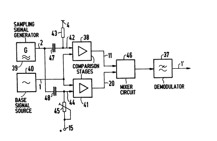
A circuit arrangement for implementing the above method is shown in Figure 3, for
the single-phase limitation embodiment. The single-phase limited output signal 1 ~, shown
at the bottom of Figure 2, is thus generated as the output signal for the circuit of Figure
; 3.
- The circuit arrangement of Figure 3 has a first comparison stage 38 having an input
connected to a delta voltage generator 39 and to a component 40 which supplies the
-6 -
2070700
base signal 1 as an output. An input 42 of the first comparison stage 38 is connected
through a resistor 43 to the base potential 4, for example ground potential.
A second comparison stage 41 is provided which also has an input connected to
the delta voltage generator 39 and to the component 40 which supplies the base signal
1. An input 44 of ~he second comparison stage 41 is connected to the first threshold
potential 15, for example via a variable resistor 45. The two comparison stages 38 and
41 have their output sides connected via a mixer circuit 46 to a means having a
demodulating effect, referred to as a demodulator 37.
In the embodiment of Figure 3, the delta voltage generator 39, for separating
voltages, is coupled to the comparison stage 38 via a capacitor 47 and is coupled to the
comparison stage 40 via a capacitor 48. Other types of coupling can be selected
dependent on the particular application. In the arrangement of Figure 3, the aggregate
signal 3 shown in Figure 2 arises only within the comparison stage 38 or 41, which may
be comparators. Consequently, the aggregate signal 3 cannot be measured (is not
formed) at the terminals of the comparison stages 38 and 41. The others signals 1, 2,
11 and 20, however, can be "seen" (measured) at the correspondingly numbered
lines.
In the embodiment shown in Figure 4, the aggregate signal 3 is already generated
before the comparison stages 38 and 41, by means of a summing element 49. In
contrast to the embodiment of Figure 3, a third comparison stage 50 is provided in the
embodiment of Figure 4 which may also be a comparator and which has its input side
connected via the summing element 49 to the delta voltage generator 39 and to the
component 40 which supplies the base signal 1. An input 51 of the third comparison
stage 50 is connected to the second threshold potential 27 of opposite polarity to the first
threshold potential 15. The threshold potentials 15 and 27 are shown in Figure 4 as being
generated by respective variable d.c. voltage sources. An input 42 of the first comparison
stage 38 is connected to the reference potential 4 (ground) and the input 44 of the
207~0
second comparison stage 41 is connected to the first threshold potential 15. The outputs
of the comparison stages 3~, 41 and 50 are connected to the mixer circuit 46. The
output of the mixer circuit 46 is connected a switching stage 52 to the means having a
demodulating effect, i.e., the demodulator 37. In bo~h the embodiments of Figures 3 and
4, the demodulator 37 is shown for exemplary purposes as a low-pass filter. In the
embodiment of Figure 4, the output signal 1~ is limited double-phase and thus generates
the output signal 1~ at its output.
The mixer circuit 46 is a multi-stage circuit. In a first mixer stage 53, which may
be an EXOR (exclusive-OR) element, the signals 11 and 20 obtained from the first and
second comparison stages 38 and 41 are mixed. In a second mixer stage 54 which may,
for example, be an OR element, the output of the first mixer stage 53 and the second
limiter signal 33 obtained from the third comparison stage 50 are mixed. Consequently,
an output signal corresponding to the control signal 11 ~ of Figure 2 is available at the
output side at the mixer circuit 46. The switching stage 52 can be driven with the control
signal 11 ~ in order to amplify the control signal 11 ~ before the base signal (modulation
signal) contained therein is available after demodulation as the output signal 1~, so that
the base signal is amplified but is also limited in amplituds.
A hearing aid 55 wherein the circuit arrangement of Figure 4 is employed is shown
in Figure 5. The component part 40 in the circuit of Figure 4, which gencrates the base
signal 1, is shown in Figure 5 as an amplifier 40 ~, to which audio signals picked up by
a microphone are supplied. The delta-shaped sampling signal 2 is formed from an
ultrasound signal generated in the hearing aid 55 by an ultrasound generator 39. The
control signal 11 ~ of Figure 2, which is available at the output of the mixer circuit 46, is
supplied to an output stage 52 operated push-pull and fashioned as a switched amplifier
(Class D amplifier). In order to enable the push-pull operation, a push-pull branch 56 is
driven via an invertor 57, as a result of which a control signal complementary to the
control signal 11 ~ is generated.
207~7~0
The switched amplifi~r 52 has four MOSFET transistors T, through T~ operating in
switoned mode. The transistors T~ and T2 are complementary transistors, as are the
transistors T3 and T4. The output stage 52 is supplied with an operating voltage via
terminals 58 and 59. Due to the switched mode, either the transistors T~ and T4 will be
simultaneously transmissive, or the transistors T3 and T2 will be simultaneously
transmissive. The time span within which these transistors palrs are transmissive Is
controlled by the pulse duration of each pulse in the control signal 11 ~. Given a changs
in the level in the control signal 11 ~, consequently, the transistors which are currenty
transmissive will change to a non-transmissive state, and the transistors which were non-
transmissive will become transmissive. As a result, the demodulator 37 in the output
stage 52 is switched between the terminals 58 and 59 according to th~ pulses in the
control signal 11 ~.
In the exemplary embodiment of Figure 5, the demodulator 37 Is an earphone 60
for the hearing aid 55. The earphone 60 contains a coil 61 finductance) which has an
integration (storing) effect due to its low-pass behavior. The higher-frequency ultrasound
components of the control signal 11~ are consequently not permitted to pass throuyh the
coil 61. An audio signal limited in amplitude can thus be obtained from the earphone 6û
as an output signal according to the curve 1~ in Figure 2.
me limitation arises due to the interruption of, for example, an original pulse having
the duration 26 by a shorter pulse having the duration 23, or by the interruption of a pulse
having the duration 36 by a shorter pulse having the duration 32, as shown in the signals
11, 21, 33 and 11 ~ of Figure 2. As a result of the additionally inserted limi~in~ pulses, the
~o,~(.qL current~at the coil 61 in the embodiment of Figure 5 cannot reach a height
(amplitude) corresponding to the original curve 1 shown in Fi~ure 1. It is therefore
important in the insertion of the limiting pulses into the signal 11 ~ that the insertion occurs
in a manner so that an existing condition (high level or low level) is interrupted by the
inserted limiting pulses. As long as this requirement Is satisfied, the mixer clrcuit 46
207~700
and/or the comparison stages 38, 41 and 50 can be formulated in ways other than that
sho..n in Figure 5 or Figure 4.
An imponant advantage of the method and circuit arrangement disclosed herein
when used in the context ol a hearing aid is that only the power which is actually required
is taken from the hearing aid battery. In conventional types o~ limiting circuits which, for
example, use a resistor for current limitation, power is lost at this resistor. Moreover, the
amplitude limitation in the method and apparatus of the invention occurs without a
decrease in amplification. No spectral spread of the signal before the pulse-width
modulator occurs, as is the case in a conventional preselection stage. Consequentiy,
oniy small reconvolution products (low distortlons) will arise in the base band (output
signal). me limiter slgnals 20 and 33 can be used as indicators that the`'circuit
~arrangomont b in ~act ~unctioning. The limitation level can be made electronically
~0 ~ gl,adlustable, for example by means of digital programming. The overall circuit arrangement
can be fully integrated in a hearing aid, i.e. no external components are required.
Although modifications and changes may be suggested by those skilled in the art,
it is the intention of the inventors to embody within the patent warranted hereon all
changes and modifications as reasonably and properly come within the scope of their
contribution to the art.
:'
-10-