Note: Descriptions are shown in the official language in which they were submitted.
20707~3
- 1
ELECTRICAL CONNECTOR
Back~round of the Invention
This invention relates to electrical connectors.
Standard electrical interconnection systems, such as the FASTECH~
5 system, usually include a plurality of circuit packs with connectors on one edge and
a backplane with compliant pins protruding therefrom. The circuit packs are inserted
into a shelf so that the connector makes electrical contact with the backplane pins.
Interconnection of the circuit packs is achieved by wires or deposited conductors
which provide electrical connection between the backplane pins. (See, e.g.,
10 Ambekar et al, "Systems Packaging" AT&T Technical Journal, Vol. 66 (July/August
1987), pp. 81-95.)
One desirable feature of such systems, especially in telecommunications
applications, is to be able to remove a circuit pack and re-route the signal from the
backplane to another circuit pack so a customer does not lose service. This can be
15 achieved by providing shorting contacts between pins so that the contacts provide
electrical connection between the pins when the circuit pack is removed but are
electrically isolated from the pins when the circuit pack is fully inserted in the shelf.
These contacts can be mounted in the backplane (see, e.g., U.S. Pat. No. 4,179,173)
or in an insulating housing surrounding the backplane pins (see, e.g., U.S. Pat. No.
20 4,070,557 and U.S. Pat. No. 4,874,333).
Since pin density is continually increasing, it is desirable to provide
shorting contacts which can be used easily in such high density applications.
Summary of the Invention
This and other objects are achieved in accordance with the invention,
25 which is an electrical connector comprising an insulating shroud including at least
one wall and a plurality of pins mounted within the shroud so that the pins extend in
a direction essentially parallel to the wall. A contact member is mounted to the wall,
the member comprising an insulating block. A spring contact comprising a tab andat least a pair of tynes at an acute angle thereto has its tabs mounted in the block so
30 that the pair of tynes make electrical contact with two of the pins.
Brief Description of the Drawin~
These and other features of the invention are delineated in detail in the
following description. In the drawing:
FIG. 1 is a perspective view of a portion of a typical electrical
35 interconnection system;
2070733
FIG. 2 is an exploded, perspective view of a connector in accordance
with an embodiment of the invention; and
FM. 3 is a top view of a portion of an interconnection system including
a connector in accordance with an embodiment of the invention.
S It will be appreciated that, for purposes of illustration, these figures are
not necessarily drawn to scale.
Detailed Description
FIG. 1 illustrates a portion of a typical interconnection system which
can utiliæ the invention. A circuit pack includes a printed circuit board, 11, on
10 which is mounted a plurality of semiconductor devices, two of which are shown as
12 and 13. Electrical conductors and other components, such as resistors and
capacitors, are not shown for purposes of clarity in the illustration. A socket-type
connector, 14, is mounted to the edge of the circuit board. The socket-type
connector comprises a housing with a plurality of apertures, each including a contact
15 which has one end bonded to conductive pads on the circuit board. The other end
includes a conductive tyne for engaging a compliant pin (see, e.g., U.S. Pat. No.
5,080,722). An array of compliant pins, only some of which, e.g., 15 and 16 are
shown, are mounted within a backplane 17. When the circuit pack is slid forward on
a rail, 18, the compliant pins will electrically engage associated contacts in the
20 socket-type connector, 14, to thereby electrically contact the components on the
circuit pack. It will be appreciated that there are usually many circuit packs mounted
on a shelf and coupled to the backplane. These circuit packs are interconnected by
conductors or wires coupled to the compliant pins on the backplane.
In order to provide re-routing of any signals to a circuit pack which has
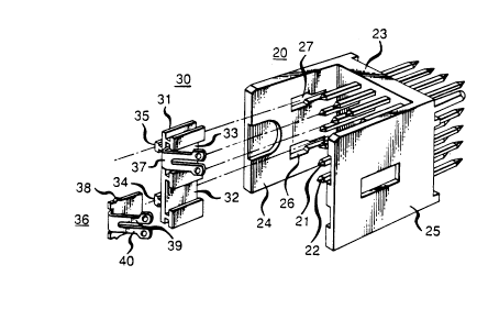
25 been removed from the shelf, the backplane connector, 20, of FIG. 2 is included.
The connector, 20, includes an array of compliant pins, e.g., 21 and 22, which are
mounted within a bottom wall, 23, of an insulating housing, hereinafter referred to
as a shroud. The shroud also includes a pair of side walls 24 and 25 which extend
from the bottom wall in a direction essentially parallel to and beyond the ends of the
30 pins. One of the walls, 24, includes a pair of slots, 26 and 27, for mounting a contact
member, 30, therein.
The contact member, 30, comprises an insulating block 31, such as a
thermoplastic polyester (30 percent glass-filled), with a pair of slots, 32 and 33,
running the width of one major surface of the block. The opposite major surface of
35 the block includes a pair of projections, 34 and 35, which mate with the slots 26 and
207!~733
- 3 -
27 in the wall 24 of the shroud to provide a bayonet-closure-type of fastening of the
member to the shroud.
A pair of spring contacts, 36 and 37, are mounted to the contact
member 30. Each spring contact includes a tab portion, e.g., 38, for inserting into a
5 slot, e.g., 32, of the contact member. The spring contact also includes a contact
portion, comprising a pair of tynes 39 and 40 formed in a plane which makes an
acute angle with the tab portion. The spring contact is typically formed from a
single piece of metal (e.g., phosphor bronze) with the contact portion folded over to
make an angle in the range 30-60 degrees with the tab portion.
When the contact member, 30, is mounted to the shroud, each tyne, 39
and 40, will make electrical contact with an associated pin, e.g., 21 and 22, so that
the two associated pins will be electrically shorted to each other.
Thus, a plurality of connectors of the type illustrated in FIG. 2 can be
mounted in a backplane (e.g., 17 of FIG. 1 minus the pins shown) by inserting
15 therein the ends of the pins directed away from the shroud. A column of such
backplane connectors would form the pin array for the socket-type connector 14 of
the circuit pack, and one or more of the backplane connectors can include the
shorting contact feature.
FIG. 3 is a schematic top view of a portion of a backplane, 17, showing
20 the two top connectors 20 and 50 in adjacent columns of such backplane connectors.
It will be noted that the circuit pack plugged into connector 50 pushes the spring
contacts off their associated pins so that the contacts rest on the insulating housing of
the socket connector (51) on the circuit pack. The spring contacts, therefore, are
electrically isolated from the pins while the circuit pack is inserted. In the adjacent
25 column, the circuit pack connector 14 has been removed from the backplane
connector 20. This causes the spring contacts to make electrical contact with their
associated pins in order to short circuit any signal intended for the removed circuit
pack. Any such signals can be re-routed, for example, to the circuit pack inserted
into connector 50. It will be further noted that the contact members, 30 and 60, are
30 mounted as close as possible to the bottom surface, 23 and 53, of the shroud and
preferably in direct contact therewith. This positioning ensures that, as the circuit
pack is removed, the spring contacts will electrically contact the pins before contact
is lost between the pins and the socket connector of the circuit pack. Thus, the signal
can be re-routed without any loss of service.
20707~3
- 4 -
It will be appreciated that although two spring contacts are shown
inserted in each contact member, any number of such contacts could be employed.
Further, each spring contact could include more than two tynes if desired. Also, the
pins contacted by the tynes of the spring contact need not be adjacent to each other.
S It will also be appreciated that the tabs of the spring contacts could be
molded into the block during an insertion molding operation, rather than inserting
the contacts into slots as shown in FIG. 2.
Various additional modifications will become apparent to those skilled
in the art. All such variations which basically rely on the teachings through which
10 the invention has advanced the art are properly considered within the scope of the
invention.