Note: Descriptions are shown in the official language in which they were submitted.
SDK, FJ-9239
`` - 2070883
WAVEFORM SYNTHE S I Z I NG C I RCU I T
BACKGROUND OF THE INVENTION
1. Field of the Invention
The present invention relates to a waveform
synthesi~ing circuit. More specifically, the invention
relates to a waveform synthesizing circuit to be employed
in a transceiver or so forth for LAN (Local Area Network)
for waveform shaping. Particularly, the invention
relates to a waveform synthesizing circuit provided in
parallel formation with a plurality of current switching
circuits for outputting a predetermined magnitude of
current when a voltage value reaches a preliminarily
assigned comparing reference voltage, and output with
superimposing currents output from a plurality of current
switching circuits for summing.
2. Description of the Related Art
For establishing mutual communication between
wordprocessors, personal computers or intelligent
terminals installed within a relatively limited area,
such as within a house or so forth, using a local area
network system (LAN).
In Fig. 1, a basic construction of the
Ethernet is illustrated as a typical example of a bus
type hAN.
In Fig. 1, a coaxial cable 3 is used as a
transmission cable. At both ends of the cable, 50 Q of
terminal resistors are provided at both ends for
impedance matching. On the other hand, depending upon
n0cessity, transceivers 2 are provided in the
transmission path of the coaxial cable 3 for enabling
communication with various terminals connected to the
coaxial cable 3. To each transceiver 2, various
terminals, such as a personal computer 6, a file server
5, printer 4 and so forth are connected, and mutual
communication is performed between personal computers 6.
Also, by the personal computers 6, the file server 5, the
2Q70~83
printer 4 or so forth are used in common. It should be
noted that, in the case of Ethernet, a so-called CSMA/CD
(carrier sense multiple access/ collision detection)
system is used to perform high speed communication with
50 ns or 100 ns of transmission pulse width employing a
manchester code in the transmission signal.
For the circuit of the transceiver 2 connecting
the terminal equipments 4 through 6 to the coaxial cable
3, the international standard IEEE 802.3 is applied to
make the waveform of the pulse current waveform smooth by
suppressing high harmonics so as to avoid noise on the
transmission path and restrict degradation of the
transmission waveform. In order to satisfy this
requirement, a waveform synthesizing circuit is
incorporated in the circuit of the transceiver 2.
One example of the conventional waveform
synthesizing circuit is illustrated in Fig. 2. This
circuit is provided with a plurality of current switching
circuits (five, a through e in the shown embodiment) in
parallel formation that output predetermined magnitudes
of currents when the voltage value of an input pulse
input to an input terminal (INl) 11 reaches respective
preliminarily assigned comparing reference voltages Vra
through Yro. The currents output from respective
plurality of current switching circuits (a) through (e)
are superimposed for summing, and the summed current is
output from an output terminal OUT 12 as the output
current. For example, the comparing reference voltages
Vra through Vr~ provided for respective plurality of
current switching circuits (a) through (e) are determined
by a predetermined current of a constant current circuit
comprising a voltage control setting terminal ~VCS) 19, a
transistor 20 and a resistor 21, voltage drops at breeder
resistors R1 through R5 by the predetermined current, and
forward voltages between bases and emitters of the
emitter follower transistors 13 to 17, which serve as low
` ~ ~ 3 ~ 207~883
impedance buffers. As an example of an assignment of the
comparing reference voltage Vr~ through Vr~, Vr. is a value
Vr~ - -5.95V determined by the summing of voltage drops
at the resistor Rl for the base-emitter forward voltage
of the transistor 18 and the base-emitter forward voltage
of the emitter follower 17 from the ground potential.
For subsequent reference voltages, by summing respective
voltage drops at respective resistors R2 to R5, the
reference voltages become Vrt = -6.0V, Vrc = -6-40V, Vrb
= -6.56 and Vr, = -6.70V.
Operation in this case will be discussed with
reference to the current switching circuit (e). When the
pulse voltage input to the input terminal INl drops below
the potential of Vr~ ~ -5.95V, an operational transistor
22 at INl side among operational transistors 22 and 23 of
the current switching circuit e turns OFF, and the
transistor 23, to which the Vro is applied, turns ON to
output (draw) current to the output terminal 12. Next,
when the pulse voltage at the input IN1 reaches Vrd = -
6.08, then the current switching circuit d becomes active
so that both currents of the current switching circuits
(d) and (e) are superimposed for summing to be output.
Similarly, the currents of respective current switching
circuits (c) to (a) are summed so that a synthesized
waveform, in which output transition waveforms are
synthesized in a stepwise fashion, is output.
Subsequently, while the input pulse voltage is rising,
the output transition waveforms are synthesized in a
stepwise fashion in opposite order. Accordingly, the
synthesized waveform, in which the pulse transition
waveform is dulled during an input pulse voltage
transition period (for example, passing period of Vra
through Vrd) passing through respective comparing
reference voltages Vra through Vr~ in order. This output
pulse is smoothed for the stepwise transition component
by a simple low pass filter at the next stage.
,-'- , ~ -
.~ . -~ ' ~ . -
~ 4 ~ 207~83
Therefore, the pulse waveform having a smooth transition
configuration at the leading and trailing edge can be
obtained.
However, the above-mentioned waveform
synthesizing circuit has the following problem.
Fig. 3 shows an output current in the case that the
above-mentioned waveform synthesizing circuit is
employed.
Fig. 3(A) shows a waveform of the input pulse
(t) at the input terminal INl, Fig. 3(C) shows an ideal
output current waveform of`the waveform synthesizing
circuit relative to the input pulse. As shown in Fig.
3(C), the waveform required is a symmetric waveform with
smooth transition portions.
However, in practice, the waveform output from
the conventional waveform synthesizing circuit is as
illustrated in Fig. 3(B). In the case of this waveform,
variation immediately after the rising and falling is
sharp and asymmetric between left and right. Therefore,
it cannot be said that the output waveform is
satisfactorily shaped, because of the wiring capacity on
the circuit board or the LSI chip or the output impedance
of the output terminal QUT 12. When an attempt is made
to reduce current consumption and make the circuit into
LSI, the above-mentioned waveform (Fig. 3(B)) becomes
more remarkable. In this case, a high harmonic component
forming the abruptly varying portion is included in the
output waveform to easily generate high harmonic noise in
the transmission path. Therefore, the signal waveform
propagating through the transmission path can be
substantially degraded.
Therefore, in view of the above-mentioned
problem, it is an object of the present invention to
provide a waveform synthesizing circuit that is
irrelative to the capacity of wiring or so forth,
satisfies the requirements for reduction of power
consumption, and provides smooth output current waveform
~ .
- - 5 - 2070883
and a high harmonic component with reduced magnitude.
SUNMARY ~F THE INVENTION
In order to solve the above-mentioned problem, the
inventor has concluded that the problem of insufficient
S waveform shaping resides in the set values of the
comparing reference voltages Vra to Vr~ assigned for
respective current switching circuits (a) to (e). The
present invention is attained based on similar setting of
the comparing reference voltage assigned for respective
switching circuits for the rise and fall of the input
pulse.
Namely, according to the present invention, there is
provided a waveform synthesizing circuit comprising a
plurality of signal output switching means for outputting
predetermined voltage magnitudes or current signals when
a voltage or a current value of an input pulse attains
preliminarily assigned comparing reference values, signal
summing means for superimposing output signals from a
plurality of the signal output switching means for
summing, comparing signal switching means detecting the
rise and fall of the input pulse, comparing reference
values with given differences between a plurality of the
signal output switching means according to the order of
operation of a plurality of signal output switching means
upon detecting rising, and comparing reference values
that are different from those for rising, with given
differences between a plurality of signal output
switching means according to an order of operation of a
plurality of signal output switching means upon the
detection of a fall.
Also, according to the present invention, the
comparing signal switching means has a delay means for
inputting the pulse with a given delay period relative to
the input pulse applied to a plurality of signal output
switching means. The delay period given by the delay
means is longer than or equal to a rising or faIling
, ~ :
- 6 - 2070~8~
period of the input pulse.
Furthermore, according to the present invention, the
given difference of the comparing reference values from
the comparing signal switching means is provided so that
the greater difference is provided near the initiation of
a transition of a rising or falling of the input signal
and a smaller difference is provided near the end of said
transition. The differences of the comparing reference
values are set by a resistor voltage divider circuit, to
which the reference voltage output from the comparing
signal switching circuit is connected in series.
As set forth above, according to the present
invention, since the comparing reference values output
from the comparing signal switching means can be set
independently for a rising and falling of the input pulse
by adjusting the difference between comparing reference
values, waveform shaping for a rising transition waveform
and a falling transition waveform can be set
independently of each other. By this, it becomes
possible to perform a waveform shaping only for a falling
transition waveform if the foregoing Fig. 3(B).
On the other hand, since the delay means provides
the input pulse signal to the comparing sigr.al switching
means with a delay longer than or equal to the rising and
falling period of the input pulse signal applied to a
plurality of signal output switching circuits, when the
pulse signal is input to the comparing signal switching
circuit, the waveform shaping for rising by respective
signal output switching means with the initially set
comparing reference values (for rising) is completed;
subsequently the comparing reference values are switched
into other values (for falling) by the input pulse, and
returned to the initial values (for rising~ after
completion of waveform shaping for falling by respective
signal output switching means. Therefore, for both a
rise and fall of the input waveform, respective
corresponding comparing reference values can be provided.
.
~ ~070883
In addition, sinee the given differenee of the
eomparing referenee values from the eomparing signal
switehing means is provided so that the greater
differenee is provided near the initiation of a
transition of a rise or fall of the input signal and a
smaller difference is provided near the end of said
transition, the waveform at initiation of transition
beeomes smooth at a greater magnitude. This is
partieularly effeetive for waveform shaping for a falling
transition waveform of the Fig. 3(B).
BRIEF DESCRIPTION OF THE DRAWINGS
Fig. 1 is a diagrammatie illustration showing an
example of a eonstruetion of a bus type LAN (Ethernet);
Fig. 2 is a eireuit diagram showing one example of a
waveform synthesi~ing eireuit employing the eonventional
transeeiver;
Fig. 3 is a ehart showing an input pulse, eurrent
waveform through the eonventional waveform synthesis;
Fig. 4 is a eircuit diagram showing one embodiment
of a waveform synthesizing circuit according to the -
present invention;
Fig. 5 is a circuit diagram showing one example of a
delay circuit to be employed between terminals INl and
IN2 of Fig. 4;
Fig. 6 is an explanatory illustration showing the
relationship between the input pulse and comparing
referenee voltages;
Fig. 7 is a ehart showing the actual measurement of
an output waveform of the transceiver employing the
waveform synthesizing circuit aecording to the present
invention;
Fig. 8 is a circuit diagram of one example of a
transmitter employing the waveform synthesizing circuit
according to the present invention; and
Fig. 9 is a circuit diagram showing one example of a
current subtracting circùit and first and second stage
ampllfying circuits of Fig. 8.
. .
;~` '. ' ' ~ ' ' : .
~ . .
` - 2070883
DESCRIPTION OF THE PREFERRED EMBODIMENT
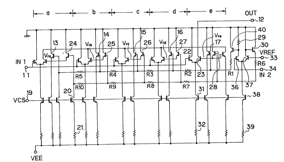
Fig. 4 is a circuit diagram showing one embodiment
of the waveform synthesizing circuit according to the
present invention. The components similar to the
foregoing prior art in Fig. 2 will be represented by the
same reference numerals. It should be noted that, in the
relationship between the present invention and the
embodiment of Fig. 4, a signal output switching means
corresponds to current switching circuits (a) to (e) of
Fig, 4; signal summing means corresponds to collector
multi-connection circuits of output transistors in the
current switching circuits (a) to (e); a comparing signal
switching means corresponds to a comparing signal
switching circuit, resistor group for setting comparing
reference values and a switching circuit for switching
two comparing reference values, as illustrated on the
right side of Fig. 4, which will be discussed later, and
a delay means corresponds to a delay circuit of Fig. 5,
which will be discussed later.
To the shown embodiment of the waveform synthesizing
circuit of Fig. 4, the outputs of five current switching
circuits (a) to (e)j which are discussed with respect to
the prior art (Fig. 2) and designed for an outputting
current having a magnitude corresponding to the
predetermined input voltage, are connected in parallel
formation. The input pulse is input parallel to the
current switching circuits (a) to (e) through an input
terminal IN1.
Next, as a representative of the current switching
circuits (a) to (e), discussion will be provided for the
current switching circuit (e). The operational
transistors 22 and 23 and transistor 31 and a resistor 32
connected to an emitter common terminal of the
transistors 22 and 23 forms a constant current circuit
and enables a high speed switching operation with a so-
called ECL (emitter coupled logic). The input pulse is
directly applied to the base of the transistor 22. On
... . ... . . .. . ... . . . . . .
...... - , .
:, . , . - . ::`. - :
.. . . .
., . - - : ~.. - : ,. :
. . . - ~ - .: - :
.,.................................... ~ :-
: . . . .
:
- - 9 - 20~883
the base of the transistor 23, the comparing reference
value, namely the comparing reference value Vr~ discussed
in the description for the prior art, is applied. By the
operational switching transistors 22 and 23, comparison
of the input pulse and the comparing reference value is
performed. The point differentiated from the prior art
is that the comparing reference voltage Vro is provided
by a diode switch circuit, to which the emitters of a
transistor 17 and a transistor 28 are connected in multi-
connection. For the bases of these transistors 17 and
28, respective one of the later-mentioned two comparing
reference voltages are applied. One of the transistors
provided a higher comparing reference voltage attains a
forward direction and turn ON and provide the comparing
reference voltage Vro.
To the base of the transistor 17, the resistor
breeder circuit, which is discussed with reference to the
prior art and formed by resistors Rl, R2, R3, R4 and R5
is connected in series. On the other hand, to the base
of the transistor 28, resistors R6, R7, R8, R9 and R10
performing a similar operation to the resistors Rl to R5,
are connected in series. In the shown embodiment, the
resistors R1 to R5 generate the comparing reference
voltage (hereafter referred to as VrOr, for example, by
adding r (rise)) to be used for a rising transition of
the input pulse applied to the input terminal IN1. On
the other hand, the registers R6 to R10 generate the
comparing reference voltage (hereafter referred to as
VrOs, for example, by adding f (fall)) to be used for a
falling transition of the input pulse.
Fig. 5 shows an example of the comparing reference
voltages relative to the input pulse. In the shown
embodiment, the respective values are set as follows:
(1) Rising of Input Pulse
V = -5.950V
V d = - 6.055V
i
:. . ..
. , : - -
lo 2Q7~
Vrcr = -6.220V
Vrbr = -6.430V
Vr~r = -6.700V
(2) Falling of Input Pulse
Vr~f = -5.950V
Vrdf = -6.195V
VrCf = -6.400V
Vrbf = -6.565V
Vraf = -6.700V
For this, in the shown embodiment, the resistors Rl
to R10 are set at the following values.
Rl = 0.625 KQ
R2 = 0.525 XQ
R3 = 0.825 RQ
R4 = 1.050 KQ
R5 = 1.350 KQ
R6 = 0.525 KQ
R7 = 1.225 KQ
R8 = 1.025 KQ
R9 = 0.825 KQ
R10 = G.675 KQ
Next, discussion will be provided for a comparing
signal switching circuit for switching two comparing
reference voltages for rising and falling.
The voltage to be input to an input terminal (IN2)
34 of the comparing signal switching circuit is the same
pulse as the pulse input to the input terminal INl set
forth above. As shown in Fig. 6, for a circuit
connecting the input terminals INl and IN2, an
appropriate delay circuit 35 is connected. It should ~e
noted that Fig. 6 shows one example of the delay circuit
~i 35 employing two inverters, but not specified thereto.
By insertion of the delay circuit 35, the transition
waveform of a rise and fall of the pulse input through
the input terminal INl is provided to IN2 with a given
delay. As shown, the comparing signal switching circuit
! . ,
11- 2~7~8~3
has essentially the same circuit construction as the
current switching circuits (a) to ~e) set forth above and
is formed by an ECL circuit of a constant-current circuit
comprising operational switching transistors 36 and 37, a
load transistor 38 and a resistor 39. For the base of
one of the transistors 36 among the transistors 36 and
37, the delayed input pulse is applied from the IN2
terminal. On the base of the other transistor 37, a
reference voltage VREF 33 to be compared with the voltage
of the input pulse is applied. In the shown example, the
comparing reference voltage at the side of the resistors
R6 to R10 to which the forward direction voltage is
applied, is fixed. In contrast, the comparing reference
voltage at the side of the resistors Rl to R5 is variable
depending upon the potential applied from a collector
load resistor 29 of the switching transistor 36 through
the emitter follower of a transistor 40.
Now, while no input is applied to the input terminal
IN2, the transistor 36 is maintaine~ at the OFF position.
In this case, the comparing reference voltage at the side
of the resistors Rl to R5 is set to be higher than the
comparing reference voltage at the side of the resistor
R6 to R10. Therefore, the comparing reference voltages
Vr~s to Vrer are supplied to the current switching circuit
(a) to (e) through the switching transistors 13 to 17.
Next, when the input pulse is applied, the transistor 36
is turned ON to lower the output voltage of the emitter
follower transistor 40. Then, the potential of the
comparing reference voltage at the side of the resistors
Rl to R5 becomes lower than that of the comparing
reference voltage at the side of the resistors R6 to R10.
By this, the comparing voltages Vr~r to Vrer are supplied
to the current switching circuit (a) to (e) through the
switching transistors 24 to 28.
~he reference voltage VREF serving as a reference
for the foregoing switching operation is set at a neutral
, .
.. : . . . . . .
,.. , . ~ ~ . : -
- 12 - 2~7~8~
position of the pulse voltage for detecting both the rise
and fall of the input pulse. Accordingly, there is the
possibility that the operation of the current switching
circuit (a) to (e) having comparing reference voltages
lower than the reference voltage VREF will become faster.
In order to solve this problem and assure the
operation of the comparing signal switching circuit, the
delay circuit 35 is inserted.
Fig. 7 shows an actually measured example of an
output current waveform according to the present
invention. In the figure, the lower waveform (b) shows
the input waveform, and the upper waveform (a) is the
output waveform obtained by a waveform synthesizing
circuit according to the present invention. It should be
noted, in the drawing, that the scale in the horizontal
direction is 50 ns/dev. and the scale in the vertical
direction is 0.5 V/div. As set forth above, according to
the present invention, the comparing reference voltages
are set independently for rising and falling to thereby
have a greater potential difference closer to the rising
and falling edge when the voltage of the input pulse
input to the input terminal INl is caused to vary
rapidly. Therefore, as can be appreciated, the sharply
varying portions are shaped into a smooth waveform.
Accordingly, according to the present invention, it
becomes possible for the output current waveform to
approach the ideal current waveform as illustrated in
Fig. 3tC). As a result, in comparison with the prior
art, the high harmonic component has been significantly
eliminated from the output current of the output terminal
OUT, and distortion of the waveform is reduced.
Fig. 8 shows one example of the transceiver circuit
for L~N for connection between the coaxial cable and the
terminal equipment by utilizing the waveform synthesizing
circuit 41 according to the present invention.
In the transceiver circuit of Fig. 8, in addition to
the waveform synthesizing circuit 41, a current
,
~. ~
-~ - 13 _ 2~70883
subtraction circuit 42, a first current amplifier 43 and
a second current amplifier 44 are used. The details of
these components are illustrated in Fig. 9/ Since the
waveform synthesizing circuit 41 has already been
discussed, here, discussion will be provided for the
current subtraction circuit 42, the first current
amplifier 43 and the second current amplifier 44 with
reference to Fig. 9.
The current subtraction circuit 42 of Fig. 9
operates using an operation reference signal from a bias
circuit formed at the left side and center portion with a
plurality of transistors, resistors or so forth. The
reference current for current subtraction is generated by
a constant current circuit formed by a transistor 46 and
a resistor 45. The reference current is output through a
buffer transistor 47 that serves to reduce the mirror
effect of the collector-base capacity of the transistor
~ 46. A difference current obtaine~d by subtracting the
l~ output current of the waveform synthesizing circuit 41
~ 20 according to the present invèntion from the output
'~ current output from the buffer transistor 47 is input to -
the first current amplifying circuit 43 at the next
stage. Accordingly, the drawing current by the waveform
synthesizing circuit 41 becomes a phase inverted output
current by the current subtraction circuit 42 and its
level is converted into a predetermined level.
The~first current amplifier 43 of Fig. 9 performs
current amplification at a magnitude approximately 80
times in combination with the second current amplifying
~ circuit 44, and serves to amplify the current 8 times.
This current amplification stage performs a so-called
differential amplifier type current amplification, and,
the output of the first current amplification circuit 43
is input to the base input of a differential transistor
49 corresponding to an inverting input terminal among
' ~ differential amplifiers 48 and 49. Furthermore, a
~ resistor 51 is connected to the emitter of an output
,i :
,,
~.
,,, , . . . , ~ -
-, . - ;;,
- 14 -
- 2Q7~8'~
transistor 50. On the other hand, a resistor 52 is
connected to a non-inverting input terminal. The other
terminals of the resistors Sl and 52 are commonly
connected to the second current amplifier 44 in the next
stage. In this case, in the voltage follower, the
voltage at the non-inverting input terminal and the
inverting input terminal become equal to each other.
Therefore, depending upon the resistance ratio of the
resistors 51 and 52, the current amplification rate is
determined. In this case, the resistance ratio, resistor
51 : resistor 52 is set at 1 : 7 to perform an 8 times
current amplification. On the other hand, a capacitor 53
of the differential amplifier is designed for a
restricting band to prevent oscillation or so forth and
equivalently serves as a low pass filter to remove the
high harmonic component from the stepwise output current
waveform of the waveform synthesizing circuit 41 to shape
into a smooth waveform.
The second current amplification circuit 44 of Fig.
9 serves amplification the remaining 10 times, in
relation to the first current amplifier 43. The output
current of the first amplifier 43 is converted into a
current in a drawing direction by a so-called current
mirror circuit comprising transistors 54 and 55 and a
resistor 56. Here, the transistors 54 and 55 are
- designed to have 1 : 10 of area ratio on a chip so that
an output current that is 10 times that of the input
current can flow. The final output stage is formed by
NPN output transistor 57 in a Darlington connection. By
this, a high impedance connection is made to the transfer
cable. It should be noted that the resistor 58 is 25Q
resistor equivalently representing 50 Q of end resistors
at both ends of the transmission cable.
Though discussion has been provided for the
preferred embodiment of the present invention, the
present invention should not be specified to the
foregoing embodiments, and, of course, is possible to be
.
'
,
. '' ~ ' -
- 15 - 2070883
modified in any way without departing from the spirit of
the invention.
By employing the waveform synthesizing circuit
according to the present invention, since the comparing
reference voltages for rising and falling are set
independently of each other, different waveform control
immediately after rising and falling becomes possible.
This enables smooth waveforms immediately after rising
and falling and therefore, a waveform synthesizing
circuit having a smooth output current waveform with
lesser high harmonic distortion.
?.
~' ,'.` 7 ~ " ,. " " , ,~ " ~" . ~
,~ , ' , , : .
.