Note: Descriptions are shown in the official language in which they were submitted.
2~71082
SWITCHING POWER SOURCE
BACKGROUND OF THE INVENTION
The present invention relates to a switching power source
applicable to various kinds of electronic apparatuses as a
stabilizing power source and, more particularly, to a switching
5 power source capable of stabilizing an output voltage with a high
transform efficiency even when an input voltage varies over a
broad range.
A switching power source is extensively used with electric
and electronic apparatuses since it is small size, light weight, '
10 and highly efficient. A switching power source has customarily
been made up a transformer, a main transistor, and a control
circuit. The transformer has a primary winding and a control
winding on the primary side and an output winding on the
secondary side. The main transistor is connected between the
15 primary side of the transformer and an input power source.
The control circuit controls the base current of the main
transistor. In operation, when the main transistor is turned
off, an output current is produced while the negative voltage on
the control winding of the transformer is rectified to generate a
20 negative voltage. The negative voltage is compared with a
-
2071082
reference voltage. The base current of the main transistor is so
controlled as to equalize the negative voltage and the reference
voltage, whereby the output voltage is stabilized. Since a
switching circuit generally has to operate without errors over a
range of input voltages of 80 V to 270 V, constants insuring the
necessary base current even when the input voltage is 80 V are
selected.
In the conventional switching power source described
above, a current proportional to the input voltage flows from
the control winding to the base of the main transistor. This
gives rise to a problem that when the input voltage is 270 V, a
current more than three times as great as the necessary base
current flows. The current more than necessary is simply
consumed by the control circuit and base resistance, degrading
the efficiency of the power source.
SUMMARY OF THE INVENTION
It is therefore an object of the present invention to
provide a simple and efficient switchinæ power source.
It is another object of the present invention to provide a
switching power source which stabilizes the output voltage at the
primary circuit side and maintains the base current constant with
no regard to the input volta~e.
A switching power source for transforming an input
~5 voltage from an input power source of the present invention has
~71 0~
a transformer made up of a primary winding, a control
winding, and at least one output winding. A switching device is
connected between the primary winding of the transformer and
the input power source. A base drive circuit has a base drive
5 capacitor connected to the base of the switching device for
storing, when the switching device is in an OFF state, an output
voltage appearing on the control winding of the transformer in
the base drive capacitor and applying, when the switching device
is in an ON state, a charge stored in the base drive capacitor to
10 the base of the switching device to thereby maintain the
switching device in the ON state. A base control circiut changes
the state of the switching device from ON to OFF. A voltage
detection circuit detects a voltage of the base drive capacitor for
feeding a corresponding control signal to the base control
1 5 circuit.
BRIEF DESCRIPTION OF THE DRAWINGS
The above and other obiects, features and advantages of
the present invention will become more apparent from the
2 0 following detailed description taken with the accompanying
drawings in which:
FIG. 1 is a circuit diagram showing a conventional
switching power source;
FIG. 2 is a circuit diagram showing a preferred
25 embodiment of the switching power source in accordance with the
20710~2
present invention; and
FIG. 3 is a circuit diagram showing an alternative
embodiment of the present invention.
DESCRIPTION OF THE PR~:FERRED EMBODIMENTS
To better understand the present invention, a brief
reference will be made to a prior art switching power source,
shown in FIG. 1. As shown, the switching power source,
generally 10, has a transformer 14 connected to an input power
source 12. The transformer 14 has a primary winding 14a and
a control winding 14b on the primary side and an output winding
1 4c on the secondary side. A main transistor 16 is connected
between the transformer 14 and the input power source 12. A
control circuit 18 includes a transistor 1 B a and a Zener diode
18b for controlling the base current of the main transistor 16.
In operation, when the main transistor 16 is turned off,
an output current is produced while the negative voltage of the
control winding 14b of the transformer 14 is rectified to generate
a negative voltage. The negative voltage is compared with a
reference voltage. The base current of the main transistor 16 is
so controlled as to equalize the negative voltage and the
reference voltage, whereby the output voltage is stabilized.
Since a switching circuit generally has to operate without errors
over a range of input voltages of 8 0 V to 2 7 0 V, constants
insuring the necessary base current even when the input voltage
20710~2
is 80 V are selected.
In the conventional switching power source 10, a current
proportional to the input voltage flows from the control winding
14b to the base of the main transistor 16. This gives rise to a
5 problem that when the input voltage is 2 7 0 V, a current more
than three times as great as the necessary base current flows.
The current more than necessary is simply consumed by the
control circuit 18 and base resistance, degrading the efficiency
of the power source.
l O Preferred embodiments of the power source switching
circuit in accordance with the present invention will be described
hereinafter with reference to FIGS. 2 and 3. In these figures,
the same or similar elements to the elements of the conventional
switching power source 10 are designated by the same reference
1 5 numerals.
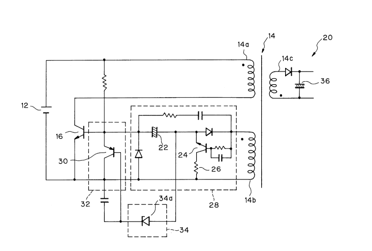
- Referring to FIG. 2, a switching power source
embodying the present invention is shown and generally
designated by the reference numeral 2 0 . As shown, the
switching power source 2 0 has a transformer 14 made up of a
20 primary winding 14a, a control winding 14b, and at least one
output winding 1 4c which are magnetically coupled to one
another. The primary winding 14a and a main transistor 16 are
connected in series and connected to an input power source 12
together. When the main transistor 16 is turned off, an output
25 current is produced from the output winding 14c. A base drive
2071082
--6--
circuit 28 has a base drive capacitor 22, a transistor 24, and a
resistor 26. When the main transistor 16 is in an OFF state, the
output of the control winding 1 4b is stored in the base drive
capacitor 22. When the main transistor 16 is in an OFF state,
5 the charge is applied from the base drive capacitor 2 2 to the
base of the transistor 16 via the resistor 2 6, thereby
maintaining the transistor 16 in the ON state. A base control
circuit 3 2 serves to change the state of the main transistor 16
from ON to OFF and is implemented by a transistor 3 0. A
10 voltage detection circuit 34 has a Zener diode 34a and detects the
voltage of the base drive capacitor 2 2 to feed a corresponding
control signal to the base control circuit 3 2 . The reference
numeral 36 designates an output capacitor.
In operation, when the voltage across the base drive
15 capacitor 22 is higher than a predetermined reference voltage set
in the voltage detection circuit 34, the transistor 30 of the base
control circuit 3 2 is turned on with the result that the base
current to the main transistor 16 is bypassed and, therefore,
reduced. Conseauently, the collector current of the main
2 0 transistor 16 is limited by a current which is h~e (current
amplificatoin factor of the main transistor 16) times as great as
the base current. Then, a counter electromotive force is
generated in the control windin~ 14b to sharply inversely biases
the main transistor 16 while charging the base drive capacitor 22
25 and output capacitor 36 to a constant voltage. In this manner,
2071082
the voltage across the base drive capacitor 22 and, therefore,
the output voltage on the secondary side of the transformer 14 is
maintained constant.
On the other hand, when the main transistor 16 is
turned on, the base current remains constant with no regard to
the voltage of the input power source 12 since the base drive
capacitor 22 is connected to the base of the transistor 16 via the
transistor 24 and resistor 26 as a power source. More
specifically, the base current of the main transistor 1 b is
prevented from increasing with the increase in the voltage of the
input power source 12.
FIG. 3 shows essential part of an alternative embodiment
of the present invention. As shown, the switching power source
has transistors 38 and 40, a capacitor 42, resistors 44, 46 and
48, and a Zener diode which in combination constitute the base
control circuit 32 for turning off the main transistor 16. The
rest of the construction is identical with the previous
embodiment. In operation, as the voltage across the base drive
capacitor 22 exceeds the reference voltage of the voltage
detection circuit 34, the transistors 38 and 40 are sequentiallY
turned on in this order. As a result, the base current of the
main transistor 16 is sharply bypassed to reverse the main
transistor 16 rapidly, insuring an efficiency even higher than the
efficiency attainable with the previous embodiment.
In summary, it will be seen that the present invention
20710~2
provides a simple and efficient switching power source which
maintains the output voltage constant at the primary circuit side
and maintains the base current constant with no regard to the
input voltage.
Various modifications will become possible for those
skilled in the art after receiving the teachings of the present
disclosure without departing from the scope thereof. For
example, the Zener diode 34a implementing the voltage detection
circuit 34 may be replaced with a shunt regulator, if desired.
Also, the main transistor 16 may be constituted by a field effect
transistor .