Note: Descriptions are shown in the official language in which they were submitted.
2~7127~
1182-9
Adlustable Resonator Arranqement
The present invention relates to an adjustable
resonator arrangement wherein the resonant frequency
can be varied, and further relates to a tunable
multi-resonator filter comprising at least one such
adjustable re~onator arrangement.
:
It is known in the high-frequency art to use resonators
of different types for different application~ depending
on the conditions of use and the desired
characteristics. Known resonator types include
dielectric, helical, strip line (including microstrip),
and air isolated rod resonators. These various
resonator types each have a relevant range of uses.
For example, dielectric resonators and filters con~
structed therefrom are commonly used, e g. in
radiotelephone applications, because of their
relatively small size and weight, stability and power
endurance. The individual resonators are in the form of
a transmission line resonator corresponding to a
parallel connection of inductance and capacitance. A
filter having the desired properties can be realised by
the appropriate interconnection o~ a number of such
resonators. For instance, a dielectric filter may be
constructed from discrete dielectric blocks, wherein an
individual resonator is for~ed in each block, or from a
single monolithic block having several resonators
formed in a common dielectric body.
It is desirable in some filter applications ~o be able to
shift the filter characteristic (i.e. the attenuation curve
of the filter~ to a higher or lower frequency wi~hout
altering the shape of the curve as far as possible. If~the
centre frequency of the filter can be adjusted between a
higher and a lower value, one adjustable filter may be used
in place of two fixed filters.
. - ., ~ ~
.
2~7 ~ 27~
It is known in the art that RF filters may be provided
with adjustment means such as adjusting screws, which
can be turned manually to alter the capacitative load
at the open end of the resonators or to alter the
inductive coupling between resonators. The individual
resonators are tuned using the adjusting screws to
obtain the desired resonant frequency and then no
further adjustments are generally made.
It is also known to automate the movement of the
mechanical adjustment means. For example, in a filter
basPd on helical resonators, a stepper motor may be
used to move an element within the electromagnetic
field and so vary the capacitative or inductive
coupling. The element may be a rod or a ring movable
within or around the helical coil, or a movable tab or
plate-like member provided at the open end of the coil.
In the case o~ a dielectric resonator, it is known to
include a variable capacitance diode at the
open-circuit end of the xesonator or within the
resonator hole. Thus the capacitive load and hence the
resonant frequency can be controlled. Such
electrically controllable resonators have the drawback
that they tend to increase the insertion loss, which is
a disadvantage because the transmission attenuation is
also increased in the bandpass region. Moreover, the
use of a variable capacitance diode may impose
limitations on the power and voltage endurance. Also,
in practice the variable capacitance diode is generally
located at an area where the field intensity of the
resonator is greatest, which may adversely affect the
coupling. Furthermore electrically adjustable filter
arrangements known in the art tend to be relatively
difficult to manufacture.
,
:, ~ ' ' ''':
.
2~27~
--3
European patent application EP-A-0,472,319 discloses a
tunable filter comprising two or more reactively
coupled dielectric resonators having voltaye controlled
tuning means, e.g. a varactor, coupled in parallel to
the open circuit end of each of the resonators
respectively. The centre frequency of the filter can
be shifted by varying the voltage applied to the tuning
means.
US Patent No. 4,186,359 discloses a notch filter net-
work compri~ing an LC parallel resonance circuit
implemented with discrete components in series with a
transmission line. The inductance is movably mounted
within a cavity resonator whose resonant frequency
differs from that of the LC circuit. The coupling
between the inductance can be varied by moviny the
inductance within the cavlty resonator causing a change
in the overall performance characteristic.
According to a firs~ aspect of the present invention
there is provided an adjustable resonator arrangement
comprising a primary resonator, and a secondary
resonator disposed within the electromagnetic field of
the primary resonator to provide electrical signal
coupling therebetween, the secondary resonator having
at least two selectable states, wherein in a first
state the secondary resonator has a first resonant
frequency, and in a second state the secondary
resonator has a second resonant frequency which is
nearer to the resonant frequency of the primary
resonator than said first resonant frequency, thereby
causing a change in the effective resonant frequency of
the primary resonator.
In a resonator arrangement in accordance with the
invention the extent to which the secondary resonator
influences the resonant frequency of the primary
'
' :' '
.
2~71271
resonator depends both on the resonant frequency of the
secondary resonator and on the intensity of the
coupling between the secondary and the primary
resonators. The intensity of the coupling is affected
by the structura of the primary resonator and the
location of the secondary resonator relative to the
primary resonator. Hence the degree of ad~ustment
(frequency shift) can be controlled according to the
particular application by suitable choi~e of the
resonant frequency of the secondary resonator and the
degree of coupling.
Suitably, the first resonant ~requency of the secondary
resonator is so difEerent from the resonant frequency
of the primary resonator that i~ has no appreciable
effect thereon.
In a particular embodiment the secondary resonator
includes adjustment means such as a pin-diode or a
varactor for selecting the two states thereof, and
means for applying a control signal to said adjustment
means, wherein the state o~ said secondary resonator is
determined by the adjustment means in response to the
control signal applied thereto.
In one state the secondary resonator may correspond to
a half-wave resonator, and in another state the
secondary resonator may correspond to a quarter-wave
resonator. This is the case, for example, when a
pin-diode is used as the adjustment means. Xn a
particular example the first resonant frequency of the
secondary resonator may be substantially higher than
the resonant frequency of the primary resonator and the
effective resonant frequency of the primary resonator
is lowered when the secondary resonator is in the state
corresponding to a quarter-wave resonator.
2 ~
A r~sonator in accordance with the invention i5
particularly suited for realization as a dielectric
resonator, more especially of the type formed from a
dielectric block having an electrode pattern provided
on a side face to allow coupling to the resonator and,
in the case of multiple resonators, between adjacent
resonators. Such a resonator configuration is
disclosed in European patent application EP-A-0,401,839
and corresponding US Patent No. 5,103,197.
Tharefore, according to a second aspect of the
invention, there is provid~d a resonator device
comprising a body of dielectric material having upper
and lower surfaces, two side surfaces, two end
surfaces, and a hole extending ~rom said upper surface
towards said lower surface; an electrically conductive
layer covering major portions of the lower surface, one
side face, both end faces and the sur~ace of said hole
thereby forming a main transmission line resonator; an
electrode pattern disposed on the other side surface
for providing electric signal coupling to and ~rom the
main resonator; and an electrically conductive strip
disposed on said other side surface forming a secondary
transmission line resonator.
The electrode pattern may be made with the aid of a
mask directly on said one side surface o~ the
dielectric block and the same ma~k may be used for
simultaneously producing the secondary strip line
resonator on the same side surface as the electrode
pattern. The length of the strip line is selected
according to the required resonant frequency.
In a praferred embodiment, means ~or adjusting the
resonant freguency of the secondary resonator are
provided on the same side surface of the dielectric block
as the electrode pattern and the strip line resonator.
.
- , ' . ' : ' '
,- '' ' ' ' -,
.~ ~
,
~127~
--6--
According to a further aspect of the invention there is
provided a filter including a plurality of resonators
wherein at least one of the resonators i~ an adjustable
resonator in accordance with the first or second
aspects of the invention. In the case of a dielectric
multi-resonator filter each of the resonators may be
formed respectively from a discrete body of dielectric
material. Alt~rnatively, some or all the resonakors
may be formed in a common body of dielectric material.
Embodiments of the invention will now be described, by
way of example, with reference to the accompanying
drawings, in which:-
Figure 1 is schematic diagram o~ a first resonatorarrangement in accordance with the invention,
Figure 2 is a perspective view of a diRlectric
resonator configuration implementing the resonator
arrangement of Figure 1, ;
Figure 3A is a schematic diagram of a different
resonator arranyement in accordance with the invention,
Figure 3B is a schematic diagram of a ~urther resonator
arrangement in accordance with the invention,
Figure 4 is a perspective view of a dielectrio
resonator coniguration implementing the resonator
arrangement of Figure 3,
Figure 5 is a graph showin~ the frequency response of
the resonators in Figure 2 and Figure 4;
Figure 6 is a schematic block diagram of a bandstop
filter in accordance with the invention,
. '
.
.
2~7~271
Figure 7 is a graph showing the frequency response of
the ban~stop filter in Figure 6,
Figure 8 is a schemakic block diagram of a bandpass
filter in accordance with the invention, and
Figure g is a graph showing the frequency response of
the bandpass filter in Figure 8.
The resonator shown in Figure 1 comprises a main
resonator Tl which can be a resonator of any suitable.
type known in the art, such as a helical, coaxial,
dielectric or strip line resonator. One end of the
main resonator (the upper end in Figure 1) is
open-circuited and the other end is short circuited to
ground potential. The resonator Tl has an inherent
resonant freq~ency f. A secondary re~onator ~2,
suitably implemented as a strip line resonator, is
provided within the electromagnetic field of the main
resonator T1. The secondary resonator is
open-circuited at its upper end, and the lower end is
short-circuited to ground potential ~ia a switchin~
element S. A reactive coupling M exerts an in~luence
between the two resonators Tl and T2.
The secondary resonator T2 has two states,
corresponding respectively with the situation when the
switching element S is open and when it is closed.
When the switching element is open, the secondary
resonator T2 acts as a half-wave resonator having a
r~sonant frequency fO. The dimensions of the strip
constituting the strip line resonator are chosen so
that its resonant frequency fo is so much higher than
the inherent resonant ~requency f of the main resonator
Tl that it has virtually no a~ct on the r~sonant
frequency of the main resonator~ After closiny tha
, ' ~
. , -
' '~
2~71 27~
switching element S, the lower end of the secondaryresonator will be short-circuited, whereby it acts as a
quarter-wave resonator with a resonant fregu~ncy of
fo/2, which is closer, but still higher than f. The
resonant frequency fo/2 is now sufficiently close to
the inherent resonant frequency f of the main resonator
that the coupling M causes the effective resonant
frequency of the main resonator T~ to shift downwards
by an amount ~f to a new re~onant ~requency ~'. The
magnitude of this frequency shift ~f can be altered as
desired by appropriate selection of the values for the
resonant ~requency fo of the secondary resonator and
the coupling M. As mentioned previously, the coupling M
is dependant on the mutual disposition o~ the primary
and secondary resonators.
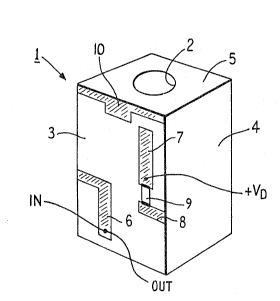
Figure 2 shows how the resonator arrangement in Figure
1 may be implemented as a dielectric resonator 1~ The
resonator is formed from a rectangular dielectric block
having a hole 2 extending from the upper face 5 to the
lower face of the block. All ~aces except the upper
face, or at least part of it around the hole 2 and the
side face 3, are coated with an electrically conductive
material which in practice is coupled to ground
potential. The non-coated side face 3 is provided with
a conductive pattern, including an L shaped strip 6
forming an orthogonal pair of transmission lines which
~ehave as a notch ~ilter. The horizontal limb of the
L-shaped strip is coupled to the conductive matsrial on
the end face of the block adjacent the side face 3, and
a common input~output point IN/OUT is present at the
remote end of the vertical limb of the ~-shaped strip
6. The upper edge of the side face 3 is also provided
with a horizontal conductive strip 10 extending to the
conductive coating on the two opposite end faces, and
having an enlarged central portion. This conductive
area 10 serves as a capacitative load for the main
.
2~127~ .
g
dielectric resonator. The dielectric coaxial resonator
thus formed has a resonant frequency f.
In accordance with the present invention, a secondary
resonator is provided in the form oP a conductive strip
7 constituting a strip line resonator. The conductive
strip 7 and a contact electrode 8 whlch is coupled to
the conductive coating on the end face 4, ars provided
as part of the conductive pattern on the same side face
~ on which the input/output coupling strip 6 is
provided.
A pin-diode 9 is connected between the lower edge of
the strip line 7 and the contact electrode 8. When the
diode 9 is non conductive, i.e. no voltage is appli~d
to the terminal connected to strip line, the strip line
7 acts as a half-wave resonator with a resonant
frequency fO significantly higher than the inherent
resonant freguency f of the dielectric resonator 1.
With the secondary resonator 7 in this state the
resonant frequency of the main dielectric resonator 1
is not a~fected thereby, as shown by the characteristic
curve Cl in Figure 5.
When the d.iode 9 is made conductive by applying a
positive direct voltage VD to the strip line, it
short-circuits the lower end o~ the strip line 7 which
therefore acts as a quarter-wave resonator. The
resonant frequency of the strip line resonator is now
much closer to that of the main resonator. This
to~ether with the coupling which occurs via the dielec-
tric material causes the characteristic curve of the
main resonator 1 to be shifted downwards by an amount
Qf resulting in the new curve C2 and the resonant
frequency o~ the main resonator is now f', see Figure
5. As shown in the exemplary curves in Figure 5, the
resulting freguency shi~t AE is approximately 2.8MHz,
.
~71 2~1
--10--
i.e. from an initial resonant frequency f of
approximately 519.3 MHz to an adjusted value ~' of
approximately 516.5 MHz.
The curves Cl' and C2' in Figure 5 illustrate the
matching of the resonator with the secondary resonator
in the first (non-adjusted) state and the second
(adjusted~ state respectively.
A second embodiment of a resonator arrangement in
accordancP with the invention is shown in Figure 3A.
The same reference numerals as before are used for the
corresponding parts. This arrangement di~fers from the
previous embodiment in that the secondary resonator T2
is permanently short-circuited at one end, at the lower
end in this case, and a switching element S i6 provided
between the other end and ground potential. When the
switch is open, the secondary resonator T2 acts as a
quarter-wave resonator having a resonant fre~uency fo.
The length of the strip line T2 is chosen such that fo
is sufficiently close to the inherent resonant
frequency f of the main resonator Tl that the effective
resonant ~requency becomes f' which is lower than f.
When the switching element S is closed, the strip line
resonator T2 is converted to a half-wave resonator with
a resonant frequency of 2*fo~ which is at such
distance from the resonant freq~lency f of the main
resonator Tl that the effective resonant frequency o~
the main resonator is unchanged (i.e. = f)O This has
the effect of increasing the resonant frequency by an
amount ~f from f~ to f.
Figure 4 shows how the resonator arrangement in Figure
3A may be implemented a~ a dielectric resonator. The
same reference numerals used in Figure 2 are again used
for corresponding parts in Figure 4. As in the first
embodiment a conductive electrode pattern is provided
-- 2071271
on the side face 3 of the dielectric block. A strip
line resonator 7 is provided as before, but in this
case the pin-diode 9 and the contact electrode 8 are
present at the upper end of the strip 7. At the lower
end of the strip line 7 there is provided an additional
vertical electrode contact strip 12 which extends to
the bottom face of the dielectric block and is
electrically connected to the conductive coating
thereon. A capacitor 11 is connected between the lower
end of the strip 7 and the electrode 120 The
capacitance of the capacitor 11 is high and its
function is to prevent a path to ~round for the control
voltage ~D applied to the strip 7. The capacitor 12
appears as a short-circuit to the radio frequency
signal. When the control voltage VD - OV, the diode 9
at the upper end of the strip is non-conductive,
whereby the strip line 7 behaves as a quarter-wave
resonator, its frequency fO being relatively close to
the frequency f o~ the main dielectric resonator. This
together with the effect of the inter-resonator
coupliny M causes the ef~ective resonant frequency to
become f' = f - ~, see attenuation curve C2 in Figure
5. When a direct voltage VD is applied to the strip
line 7, the diode 9 becomes conductive and connects the
upper end o~ the strip 7 via the contact electrode 8 to
ground potential. The strip line 7 now behaves as a
half wave resonator with a resonant frequency of 2*fo~
this being significantly higher than the frequency o~
the main resonator, and as a result, the resonant freq-
uency of the main resonator effectively increases by an
amount ~f to f, which is in fact the inherent
(unadjusted) resonant frequency of the main resonator.
The corresponding attenuation curve Cl has thus been
shifted upwards, as shown in Figure 5.
In view of the foregoing description it will be evident
to a person skilled in the art that other resonator
.
.
~7~27~
-12
arrangements may be made within the scope of the
present invention. For example a reactive load may be
provided at the opposite end of the secondaxy resonator
from the switching element, in order to set the
frequency of the secondary resonator at a desired
level~ Using an appropriate load the resonant
frequency of the secondary resonator can be positioned
below the resonant frequency of the main resonator. In
this case the frequency shift ~ may be positive
between the non-adjusted and adjusted values, i.e. the
adjusted value may be greater than ths inherent
resonant frequency of the main resonator.
In another embodiment, shown schematically in Figure
3B, one end of the strip line 7 may be connected to
ground potential and the other end may be connected via
a switching element S to a conductive strip 15 havin~
an open circuit at its opposite end. In this way, not
only the resonant frequency of the secondary resonator
T2, but also the coupling between the secondary res-
onator and the main resonator can assume two di~erent
values M, M' depending on the switch posit.ionsO
Consequently, the effective resonant frequency of the
main resonator will again have two different values,
but n this case there will be a contribution not only
from the different resonant frequencies of the
secondary resonator, but al50 the different levels of
coupling M, M'.
Furthermore, the ~ize and location of the strip line
resonator on the side ~ac~ of the dielectric resonator
can be selected according to the fre~uency and coupling
requirements. Moreover, an element other than a diode
may be used as the switching element. Also, the
switching element may be provided externally or
remotely from the main re~onator in which case a
conductive lead connected to the secondary resonator
:' .
,
~ 2 ~ P~ 7 ~
-13-
may be used to make the external connection to the
switching means.
It is not necessary for the secondary resonator to be
provided on an integral part of the main resonator as
in the case of the dielectric block filter described
above. Alternatively the secondary resonator may be
supported on a separate insulating plate. For example
in the case of a helical main resonator a secondary
helical resonator may be supported on an insulating
plate adjacent the main helix. Such an insulating
plate may also be used in the context o~ a diel~ctric
filterO
An electrically controllable resonator in accordance
with the invention offers a number of advantages in
comparison with known resonators. For example, the
secondary resonator can be very small in size and is
preferably realized as a strip line. The overall
resonator arrangement can thus be very aompact since
the components used for adjustment n~ed not occupy
extra space in the main resonator structure, so that
the size of the resonatQr filter can be smaller than ~`
its prior art counterparts. The ~lectrical properties
of the resonator can be altered by appropriate design
and if a variable-capacitance diode (varactor) is used
for the switching element, the characteristic curve can
be shifted continuously or incrementally over a certain
range depending on the applied voltage. Also, the
number of the resonators used in a multi-pole ~ilter
may be reduced because a wider band of filtering may
be achieved with these resonators. This means not only
a saving in material but also a smaller, lighter
filtex.
It is noted here that resonator arrangements in
accordance with the invention may be combined in
: -
2~71~7~
various ways to form tunable filters having differentfrequency responses.
For example there i5 shown in Figure 6 a 2-pole tunable
bandstop filter comprising a pair of similar
inductively inter-coupled resonator arrangem~nts
analagous to those described above with reference to
Figuxes 1 and 2. In this cas~ the switching element S
coupled between the lower end o~ the secondary
resonator T2 and ground potential is a respectiYe
varactor. The upper end of each secondary resonator T2
is coupled via a respective 100 kohm resistor R to a
common point at which a control voltage VD may be
applied. The input signal is coupled into the lefthand
main resonator T1 by means of an L-~haped pair of
strips Ll,L2 forming an orthogonal pair of transmission
lines in a similar manner to the Figure 2 embodimen~.
Likewise, the signal output terminal is couple~ to the
righthand main resonator Tl by means of an L-shaped
pair of strips L3,L4 also forming an orthogonal pair of
transmission lines. The two pairs of orthogonal
transmission lines Ll,L2 and L3,L4 have a notch efect
which influences the overall shape o~ the ~îlter
characteristic. Also, respective capacitor~ Cl and C2,
typically having a value o~ 3pF, are coupled between
the lower end of the strips L2 and L4 respectively and
ground potential~ The lower ends of the strips L2 and
L4 are also intexcoupled by a transmission line strip
L5 which provides inductive coupling between the
resonator arrangements. The capacitors C1 and C2
together with the strip L5 help to provide additional
low pass filtering.
The characteristic curves for this 2-pole bandstop
filter are shown in Figure 7, wherein the curves
Kl,K2,K3,K4 correspond with a control voltage VD of
lV,2V,3V and 4V respectively.
. ... : .
.. . .
.,, .. - . . - . ..
2071271
-15-
In Figure 8 there is shown a 3-pole tunable bandpass
~ilter comprising three int6r~coupled resonator
arrangements of the type described above with reference
to Figure 1 and 2. As in the bandstop filter of Figure
6, a respective varactor S is coupled between the lower
end of each secondary resonator T2 and ground
potential. Similarly, the upper end of each secondary
resonator is coupled via a respective 100 kohm resistor
R to a common point at which a control voltage VD may
be applied. The upper ends of the adjacent main
resonators are coupled via capacitors C3, C4. The
input signal is coupled to the lefthand main resonator
Tl by means of a transmission line strip L6, the upper
end of which is coupled to a further transmission line
strip L7. The strip L7 in turn provides coupling into
the central resonator. Coupling from the righthalld
resonator for the signal output is provided again by an
L-shaped pair of strips L8,L9 forming an orthogonal
pair of transmission lines as in the bandstop
embodiment of Figure 6. The outer end of s~rip ~9 is
coupled directly to ground potential and the outer end
o~ strip L~ is coupled to ground potential via a
capacitor C5.
The characteristic curves representing the frequency
response for this 3-pole bandpass filter as the applied
voltage YD is varied are shown in Figure 9, wherein the
curves Jl~J2~J3 and J4 correspond with a control
voltage VD of lV,2V,3V and 4V respectively.
Finally it is noted that other filter variants are
possible within the scope of the claims. For example,
in a multi-resonator filter not all of the main
resonators but only selected resonators sr groups of
resonators may include secondaxy resonators in
accordance with the invention.
'
.
.
. ~: