Note: Descriptions are shown in the official language in which they were submitted.
SATELLITE TELEVISION BROADCASTING RECEIVER
The present invention relates to a satellite television broadcasting receiver to be
used for receiving satellite television broadcasting in accorclance with a communication
satellite or a bro~dc~sting sateliite.
In recent years, communication services utilizing a communications satellite (CS)
have come to be provided extensively. A satellite television broadcasLi"g receiver which is
used for the purpose of receiving pictures and television broadcasting programs offered by
10 utilizing satellites has basically the same structure as that of the receiver for receiving
television broadcasting proyldms according to a broadcasting satellite, as is known in the
prior art discussed hereinafter.
It is an object of the present invention to provide a satellite television broadcasting
receiver which can reproduce images in a satisfactory condition by eliminating a flickering
interference that occurs due to the nonlinearity of the amplifier even in the case of a
television broadcasting according to a communications satellite where the level of the
energy dispersal signal superposing on the image signal is large.
In order to achieve the above object, there is provided in accordance with one
aspect of the present invention a satellite television broadcasting receiver comprising;
a channel selecting circuit for receiving, as an input signal, a first intermediate
frequency signal obtained by frequency converting a plural channel of radio waves received
from a satellite and for frequency converting the first intermediate frequency signal into a
-1 -
~ 7 ~
second intermediate frequency signal such that a selected channel of the second
intermediate frequency signal has a predetermined frequency;
a band-pass filter for receiving the second intermediate frequency signal and for
passing therethrough only a desired FM signal of the selected channel of the
second intermediate frequency signal;
an FM demodulator for demodulating the desired FM signal so as to obtain a pre-
emphasized video signal which has been pre-emphasized at a transmitter;
a de-emphasis circuit for de-emphasizing the pre-emphasized video signal;
a low-pass filter~ receiving an output signal of the de-emphasis circuit, for passing
~0 therethrough only a video signal;
a first amplifier for amplifying the video signal from the low-pass filter and outputting
an amplified video signal;
a first clamping circuit for clamping the amplified video signal and outputting a
clamped video signal;
a second an,plirier for amplifying the clamped video signal and outputting a second
amplified video signal; and
a second clamping circuit for clamping the second amplified video signal and
outputting a second clamped video signal;
wherein each of the first cla",p..,g circuit and the second clamping circuit has an
~0 input terminal and an output terminal and each comprises:
a capacitor connected at a first end to the input terminal and connected at a second
end to the output terminal;
a DC power source; and
-
20 7 ~ ~ ~ 3
a transistor having an emitter connected to the output terminal and a base
connected to the DC power source.
With the above-described structure, the satellite tclcvision bro~dc~-sting receiver of
the present invention inputs to the first clamping circuit, at a low level, an image signal
superposed with an energy dispersion signal which is larger than that of a bro~dc~sting
satellite, to eliminate the energy dispersion signal, and provides a room to the dynamic
range of the later-stage amplifier to keep the DG and DP of the later-stage amplifier in a
satisfactory condition in the second clamping circuit. Thus, even in the case of receiving a
10 television broadcasling according to a communications satellite in which the level of the
energy dispersion signal superposing on the image signal is large, it is possible to
substanlially reduce the distortion which occurs due to the nonlinearity of the amplifier and
satisfactorily reproduce the video without receiving a flickering interference.
Further, in order to solve the above-described problem, the satellite television
broadcasting receiver of the present invention includes a pulse extracting circuit for
extracting a synchronizing signal of an input image signal which has been obtained by FM
demodulating and deemphasizing the waves received from the satellite television
broadcasting and then passing the waves through the low-pass filter, a switching circuit for
20 clamping the image signal based on the output signal of the pulse extracting circuit, the
pulse extracting circuit and the s~l~itchi"g circuit forming a pulse clamping circuit, an
amplifier for amplifying the output of the pulse clamping circuit, and a clamping circuit for
having the output signal of the amplifier as an input and clamping the video signal.
2 0 7 ~ 2 8 3 -~
With the above-described structure, according to the present invention, a video
signal of the satellite telcvision broadcA~,li"g that has been received and demodulated is
de-emphasize so that the frequency characteristics are flattened to be equivalent to those
of the original signal, and the noise component of the wide band generated in the
transmission system is eliminated by the low-pass filter. Then, the image signal is inputted
to an energy dispersion signal eliminating unit consisting of the pulse clamping circuit, the
amplifier and the peak clar"r.ng circuit so that the energy dispersion signal is eliminated.
The image signal after having the energy dispersion signal eliminated is then impedance
converted by the buffer a",F!ifier and a low impedance is outputted in a drivable state.
In this case, a synchronizing signal necessary for pulse clamping is extracted, by
the pulse extracting circuit, from the video signal which has been inputted to the energy
dispersion signal eliminating unit. The synchronizing signal extracted is inputted to the
switching circuit and the video signal is fixed to the reference voltage only during the pulse
period of the synchronizing signal, to achieve the pulse clamping. The energy dispersion
signal need not be completely eliminated, and it is important that no distortion occurs in the
video signal due to the influence of nonlinearity of the amplifier connected to the next
stage. The video signal has a sufficiently lower level than, for example, the level inputted
to the peak clamping circuit at the later stage. Therefore, the pulse cla",r ng circuit which
20 does not apply any distortion to the video signal even at the low level is suit~ ~!e.
The video signal which has been amplified to 2 Vp-p by the amplifier is inputted to
the clamping circuit. Since the energy dispersion signal is finally sufficiently eliminated by
-
~a 7 ~ 2 8 ~
this cla"~ping circuit, it is possible to provide the energy dispersion signal eliminating unit
which can be sufficiently used for the satellite television broadcasting according to the CS.
In accordance with a further aspect of the present invention, there is provided a
satellite television bro~dc~sting receiver comprising:
a channel selecting circuit for receiving, as an input signal, a first intermediate
frequency signal obtained by frequency converting a plural channel of radio waves received
from a satellite and for frequency converting the first intermediate frequency signal into a
second intermediate frequency signal such that a selected channel of the second
~0 intermediate frequency signal has a predetermined frequency;
a band-pass filter for receiving the second intermediate frequency signal and for
passing therethrough only a desired FM siqnal of the selected channel of the second
intermediate frequency signal;
an FM demodulator for demodulating the desired FM signal so as to obtain a pre-
emphasized video signal which has been pre-emphasized at a transmitter;
a de-emphasis circuit for de-emphasizing the pre-emphasized video signal;
a low-pass filter, receiving an output signal of the de-emphasis circuit, for passing
therethrough only a video signal;
a first amplifier for amplifying the video signal from the low-pass filter and outputting
~0 an amplified video signal;
a pulse clamping circuit, comprising:
an input terminal receiving the amplified video signal from the first amplifier
and an output terminal,
-5 -
~ 0 ~ 3
a switching circuit connected to the input terminal and selectively providing a
consldnl voltage to the amplified video signal that is input to the input terminal, in
accordance with a control signal,
an inversion amplifier receiving the anlpliried video signal and providing an
output based on inversion amplifying the amplified video signal,
a peak holder circuit for receiving the output of the inversion amplifier and
providing an output representing a peak of the output of the inversion amplifier,
a level shifter circuit for receiving the output of the peak holder circuit and
shifting a level thereof by a given amount to obtain a level shifted output, and
a comparator for comparing the level shifted output of the level shifter circuit
to the output of the inversion amplifier and generating the control signal in
response thereto;
a second amplifier for amplifying the video signal clamped by the switching circuit
and outputting a second amplified video signal; and
a clamping circuit for clamping the second amplified video signal output from the
second amplifier so as to output a clamped video signal.
Having thus described the invention, reference will now be made to the
accompanying drawings, illustrating preferred embodiments and in which:
Fig. 1 is a block diagram illusl,aling the sat~";t~ television broadcasting receiver
according to one embodiment of the present invention;
Fig. 2 is a circuit diagram illusl,alillg the clan,ring circuit;
-6-
, i
Fig. 3 is a block diagram illusl,dti"g the conventional satellite televisionbro~dc~ting receiver;
Fig. 4 is a waveform diag,dm illusl,ali"g an image signal on which the energy
clisper~ion signal of which frequency shift is 600 khzp-p has been superimposed;
Fig. 5 is a waveform diagram illuslldling the image signal on which the energy
dispersion signal whose frequency shift is 3 MHzp-p has been superposed;
Fig. 6 is a diagram illusl,aling the receiving system of the satellite televis,on
bro~dcasl;ng receiver including the energy dispersion signal eliminating unit according to
one embodiment of the present invention;
Fig. 7 is a block diagram illustrating the pulse clamping circuit which structures a
part of the energy diffusion signal eliminating unit according to one embodiment of the
present invention;
Fig. 8 is a circuit diagram illustrating the peak clamping circuit which structures a
part of the energy dispersion signal eliminating unit according to one embodiment of the
20 present invention;
Fig. 9 is a configuration diagram illustrating the pulse clamping circuit which is used
in the present invention; and
-
~ 7 ~ 2 ~ 3
Fig. 10 is a .liagra", illustrating the waveform of each portion of the pulse clamping
circuit shown in Fig. 1.
Similar numerals denote similar elements.
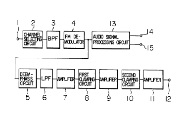
Figures 3 through 5 represent prior art. Referring initially to Fig. 3 shown is a prior
art arrangement. Numeral 1 designates an input terminal for inputting a first intermediate
frequency signal. The input terminal 1 frequency converts radio waves of a 12 GHz band
which have been received from a satellite by an antenna into a frequency of 1 GHz band by
10 a down converter and applies a first intermediate frequency signal guided into the indoor
by a coaxial cable. Numeral 2 designates a channel selecting circuit for receiving signals
of one channel by selecting one broadcasting station out of multiple first intermediate
frequency signals. Numeral 3 designates a band-pass filter for passing only one wave out
of output signals of the channel selecting circuit 2. Numeral 4 designates an FM
demodulator for demodulating an FM signal which is an output signal of the band-pass filter
3. Numeral 5 designates a deemphasis circuit for deemphasizing a demodulator output
signal which is an output of the FM demodulator 4. Numeral 6 designates a low-pass
filtering circuit for passing only a video signal and numeral 20 designates a first ar"F';rier for
amplifying the output signal of the low-pass filtering circuit 6. Numeral 21 designates a
20 clamping circuit for removing an energy dispersion signal included in the output signal of
the first amplifier 20. A second amplifier 22 for amplifying the output of the clamping circuit
21; numeral 12 designates a video signal output terminal for outputting the output signal of
the second amplifier 22. An audio signal processing circuit 13 is provided for outputting an
audio signal from a demodulator output signal which is an output of the FM demodulator 4.
-8 -
~ 0 ~ 3
Numerals 14 and 15 designate audio signal output terminals for outputting output signals of
the audio signal processing circuit 13.
The operation of the satellite television broadcasting receiver having the above-
described structure will be explained below. A first intermediate frequency signal, guided to
the indoor by a coaxial cable, which has been obtained by frequency converting the waves
of 12 GHz band received by the antenna from the satellite into the frequency of 1 GHz by
the down converter, is applied to the input terminal 1. By selecting one broadcasling
station by the channel selecting circuit 2, signals of only one channel are received out of
10 multiple first intermediate frequency signals. Out of the signals selected through the
channel selection by the channel selecting circuit 2, only one wave is passed by the band-
pass filter 3. A SAW filter is generally used for the band-pass filter 3. The FM demodulator
4 demodulates the FM signal of the selected channel, to obtain a demodulator output
signal. The audio signal processing circuit 13 demodulates an audio signal which has been
QPSK modulated in the sub-carrier of 5.7 MHz from the demodulator output signal. After
PCM demodulating the signal, the audio signal processing circuit 13 converts a digital
signal into an analog signal by a D/A converter, and outputs the audio signal to the audio
signal output terminals 14 and 15 respectively through the low-pass filter. The demodulator
output signal of the FM demodulator 4 is inputted to the deemphasis circuit 5 to flatten the
20 frequency characteristics of the signal that has been pre-emphasized by the transmitter.
The signal that has been flattened by the deemphasis circuit 5 is inputted to the low-pass
filtering circuit 6 so that only the image signal is passed and outputted by the low-pass
filtering circuit 6.
The spectrum of the FM demodulator by the video signal becomes such that energy
is concer,l,ated around the frequency corresponding to a pedestal level or a synchronizing
signal level which have a large time factor in the video signal level, having a peak of
electric power in this energy concentrated region. Since this peak interferes with the
microwave circuit such as a telephone line, the WARC-BS has prescribed that the power
flux density of satellite waves is lowered by 22 dB in the band width per 4 KHz. This is
called energy dispersion which is achieved by superimposing a triangular wave
synchronous with the frame frequency on the video signal. In the case of a sate":tc
television bro~dcasli.,g according to a broadcasting satellite, the frequency shift of the
10 energy dispersion signal is 600 KHzp-p and the repetition frequency of the energy
dispersion signal is 15 Hz. Since the frequency shift of the main carrier is 17 MHzp-p, the
level of the energy dispersion signal which is superposed on the video signal 1 Vp-p
becomes 0.11 Vp-p when the pre-emphasis applied to the video signal is taken into
account. Fig. 4 shows the state of the video signal on which the energy dispersion signal
has been applied in the case of television broadcasting according to a broadcasting
satellite. (Reference document: A Satellite Broadcasting Receiver [Part 2, Desirable
Performance]; The Radio Engineering and Electronics Association.)
In recent years, there have been various schedules for carrying out a television
20 bro~dc~sling by using communications satellites. In this case, more severe conditions
have been prescribed for these communications than those for a satellite broadc~sting. In
the case of a television broadcasting in Japan based on a communications satellite, the
frequency shift of the energy dispersion signal is in the range from about 2 MHzp-p to
about 3 MHzp-p and the repetition frequency of the energy dispersion signal is a triangular
-10-
,~;.
~i "3,
- 20~283
wave of 30 Hz. Since the frequency shift of the main carrier is different depending on the
satellite, the level of the energy dispersion signal superposing on the video signal 1 Vp-p is
about 0.5 Vp-p at maximum when the pre-emphasis applied to the video signal is taken into
account. Fig. 5 shows a state of the video signal on which the energy dispersion signal is
superposed in the case of television broadcasting according to a communications sate";tc.
On the image signal which has been FM demodulated, de-emphasize and passed
through the low-pass filter, the energy dispersion signal has been kept superposed. When
the video signals are reproduced on the screen in this state, a flickering interference occurs
10 on the signal.
When the output signal of the low-pass filtering circuit 6 is applied as an input, the
first amplifier 20 amplifies the signal to 2 Vp-p in the level of the image signal excluding the
portion of the energy dispersion signal and produces the result as an output. The clamping
circuit 21 eliminates the energy dispersion signal which has been superposed on the video
signal and applies a DC bias to the second amplifier 22. The second amplifier 22 is a
buffering circuit in which the voltage gain is 1. A DC bias of satisfactory DG and DP is set
by the clamping circuit 21 and the video signal of 1 Vp-p is outputted in the terminal value
of 75 n from the video signal output terminal 12.
According to the above-described structure, however, the level of the energy
dispersion signal which is superposed on the image signal 1 Vp-p is about 0.5 Vp-p at
maximum in the case of television broadcasting according to a communications satellite.
Thus, in the case of receiving a television broadcasting according to a communications
-11-
2 ~ 3
satellite, the value between the peaks of the video signal on which the energy dispersion
signal has been superposed is larger than that in the case of a broadcasii.,g satellite. As a
result, a distortion occurs because of the nonlinearity of the first amplifier. Even if the
energy dispersion signal can be completely removed by the clamping circuit, a flickering
interference occurs on the screen of the reproduced picture due to this distortion.
Referring to Fig. 1, numeral 1 designates an input terminal of a first intermediate
frequency signal, numeral 2 a channel selecting circuit, numeral 3 a band-pass filter,
numeral 4 an FM demodulator, numeral 5 a deemphasis circuit, numeral 6 a low-pass
filtering circuit, numeral 13 a voice signal processing circuit and numerals 14 and 15 audio
signal output terminals. The above components are the same as those in Fig. 3.
Numeral 7 designates a first amplifier for amplifying an output signal of the low-pass
filtering circuit 6. Numeral 8 designates a first clamping circuit for eliminating the energy
dispersion signal included in the output signal of the first amplifier 7. A second amplifier 9
is for amplifying the output signal of the first clamping circuit 8; numeral 10 designates a
second clamping circuit for DC reproducing the output signal of the second amplifier 9 and
applying a DC bias to a buffer amplifier 11. The buffer amplifier 11 amplifies the output
signal of the second clai"F..,g circuit 10. Numeral 12 designates a video signal output
terminal for outputting an image signal which is the output signal of the buffer amplifier 11.
The operation of the satellite broadcasting receiver having the above-described
configuration will be explained below with reference to Fig. 1. First, waves of a 12 GHz
band from the satellite received by the antenna are frequency converted into a 1 GHz band
by the down converter and then guided to the indoor by the coaxial cable to provide a first
-12-
-
2 ~ ~
intermediate frequency signal. The first intermediate frequency signal is applied to the input
terminal 1. Out of multiple first intermediate frequency signals received by the antenna,
the channel selecting circuit 2 receives one channel by selecting one bro~dcasting station.
Of the signal selected by the channel selecting circuit 2, only one wave is passed by the
band-pass filter 3. A SAW filter or the like is generally used for the band-pass filter 3. The
FM demodul?tor 4 demodulates the FM signal of the selected office and obtains a
demodulator output signal. The audio signal processing circuit 13 demodulates an audio
signal, which has been obtained by QPSK modulating the demodulator output signal into a
sub-carrier of 5.7 MHz, then PCM demodu~ates this voice signal, converts the digital signal
10 into an analog signal by the D/A converter, and outputs the audio signal to the audio signal
output terminals 14 and 15 through the low-pass filter respectively. The demodulator
output signal of the FM demodulator is inputted to the deemphasis circuit 5 so that the
signal pre-emphasized by the transmitter is restored to the original state by this circuit 5 by
flattering the frequency characteristics. The signal of which frequency characteristics have
been flattened by the deemphasis circuit 5 is inputted to the low-pass filtering circuit 6 so
that only the video signal is passed and outputted by the low-pass filtering circuit 6.
The first amplifier 7 amplifies the output video signal of the low-pass filtering circuit 6 to the
level necessary for operaling the clamping circuit 8, and then outputs the amplified video
signal.
The first clamping circuit 8 eliminates the energy dispersion signal superposed on
the video signal by the clamping operation, and outputs the video signal. The second
amplifier 9 amplifies the output signal level of the first clamping circuit 8 to 2 Vp-p and
outputs the amplified signal. The second cla,np..,g circuit 10 DC reproduces to apply a DC
-13-
-
~ 7 ~ 7. ~ ~
bias to the buffer an,~!irier 11. The buffer amplifier 11 is the buffering circuit of which
voltage gain is 1. A DC bias of which DG and DP are satisfactory is set by the second
clamping circuit 10 and the video signal of 1 Vp-p at a terminal value of 75 n is outputted
from the video signal output terminal 12.
Fig. 2 shows one example of the clamping circuit used in the first clamping circuit 8
and the second clamping circuit 10. Referring to Fig. 2, numeral 31 designates an input
signal terminal to which a signal is applied, numeral 32 designates a capacitor one end of
which is connected to the input signal terminal 31, numeral 33 designates an output signal
10 terminal, numeral 34 designates a DC power source, numeral 35 designates a l,dnsistor of
which base is connected to the DC power source 34 and the emitter is connected to the
other end of the capacitor 32 and the output signal terminal 33, and numeral 36 designates
a power source terminal. The DC component is cut off from the input signal applied to the
signal input terminal 311 by the caracitor 32. When the difference of voltage between the
one connected to the signal output terminal 33 of the capacitor 32 and the voltage of the
DC power source 34, or the voltage between the base and the emitter of the transistor 35,
becomes larger than 0.6 V because of the change of the amplitude of the input signal, the
llansistor 35 becomes conductive and the capacitor 32 is charged. As a result, at the
signal output terminal 33, the DC potential of the peak value at the negative side of the
20 input signal is clamped to the voltage which is about 0.6 V below the voltage of the DC
power source 4.
As explained above, according to the present embodiment of the present invention,
the sate" te television bro~dc~sting receiver includes the channel selecting circuit for
-14-
~ ~ 7 ~ ~ ~ 3
having an input signal of a first intermediate frequency signal which is obtained by
frequency converting the waves received from the satellite, the band-pass filter for having
the output of the channel selecting circuit as an input and passing only a desired FM signal,
the FM demodu~ator for inputting the output signal of the band-pass filter, the deemphasis
circuit for having the demodulator output signal of the FM demodulator as an input and
deemphasizing the signal which has been pre-emphasized by the transmitter, the low-pass
filtering circuit for having the output of the deemphasis circuit as an input and passing only
the video signal, the first amplifier for having the output of the low-pass filtering circuit as
an input and amplifying this signal, the first clamping circuit for having the output of the first
10 amplifier as an input and clamping this signal, the second amplifier for having the output of
the first clamping circuit as an input and amplifying this signal, the second clamping circuit
for having the output of the second amplifier as an input and clamping this signal, and the
buffer amplifier for having the output of the second clamping circuit as an input and buffer
amplifying this signal. With this ar,angement, even in the case of the television
broadcasl;ng according to the communications satellite in which the level of the energy
dispersion signal superposing on the video signal is large, the video signal on which the
energy dispersion signal larger than that according to the broadcasting satellite has been
superposed is inputted to the first clamping circuit at a low level, to thereby eliminate the
energy dispersion signal so that a room is provided in the dynamic range of the amplifier at
20 the later stage. The operating point of the buffer amplifier is decided by the second
clamping circuit, to keep the DG and DP in a satisfactory condition. Thus, the influence of
the nonlinearity of the amplifier can be reduced substantially and the image can be
reproduced satisfactorily on the screen without having an interference of flickering.
-15-
As explained above, according to the present invention, the satellite television
bro~dc~cting receiver includes the channel selecting circuit for having an input signal of a
first intermediate frequency signal which is obtained by frequency converting the waves
received from the s~te'l le, the band-pass filter for having the output of the channel
selecting circuit as an input and passing only a desired FM signal, the FM demodulator for
inputting the output signal of the band-pass filter, the deemphasis circuit for having the
demodulator output signal of the FM demodulator as an input and deemphasizing the
signal which has been pre-emphasized by the transmitter, the low-pass filtering circuit for
having the output of the deemphasis circuit as an input and passing only the video signal,
10 the first amplifier for having the output of the low-pass filtering circuit as an input and
amplifying this signal, the first clamping circuit for having the output of the first amplifier as
an input and clamping this signal, the second amplifier for having the output of the first
clamping circuit as an input and amplifying this signal, the second clamping circuit for
having the output of the second amplifier as an input and clar"p.ng this signal, and the
buffer amplifier for having the output of the second clamping circuit as an input and buffer
amplifying this signal. With the above arrangement, even in the case of the television
broadcasting according to the communications satellite in which the level of the energy
dispersion signal superimposing on the video signal is large, the satellite television
broadc~sli"g receiver can be provided which su6star,lic.lly reduces the influence of the
20 nonlinearity of the amplifier and reproduces the image on the screen in a satisfactory
condition without an interference of flickering.
A second embodiment of the present invention will be explained with reference to
the drawings. Fig. 6 is a block diagram for showing the receiving system of the s~te'l;te
-16-
. _
tclcv;sion broadcasli,lg receiver according to the second embodiment of the present
invention. Referring to Fig. 6, numeral 1 designates an input terminal for inputting a first
intermediate frequency signal, numeral 2 designales a channel selecting circuit, numeral 3
designates a band-pass filter, numeral 4 designates an FM demodu'~or, numeral 5
designates a deemphasis circuit, numeral 6 designates a low-pass filter (LPF), numeral 7
designdles a first amplifier, numeral 11 designates a buffer amplifier, numeral 12
designates a video signal output terminal, and numerals 14 and 15 designate voice signal
output terminals (R, L), all of which have the same functions as those of Fig. 1.
Numeral 20' designates an energy dispersion signal eliminating unit, which consists
of a pulse clamping circuit 21 which has an input of the video signal outputted from the first
amplifier 7, extracts a synchroni~alion signal from this video signal and fixes the video
signal to a reference signal only during the pulse period of the synchronization signal by
using this synchronizing signal, a second amplifier 9 for amplifying the output signal of the
clamping circuit 21 and a clamping circuit 10 for clan,p.ng the video signal outputted from
the second amplifier 9. The second amplifier 9 and the clamping circuit 10 are the same as
those of the first embodiment.
The pulse clamping circuit 21 is structured by an inversion amplifier, a pulse
20 detecting part consisting of a peak holder, a level shifter and a comparator, a voltage
source and a switch, as shown in Fig. 9. The operation of the pulse clamping circuit 21 will
be explained with reference to Fig. 10. When a video signal as shown in a waveform
diagram O is inputted to the input terminal, the video signal is inversion amplified by the
inversion amplifier. Since the rererence voltage of this inversion amplifier is a clamp
-17-
voltage of the tip of a sy"chroni~;"9 signal level, the output of the inversion amplifier takes
an amplified pattern of the synchronizing pulse portion and a part of the burst signal as
shown in a waveform diagran, ~. When the output of the inversion amplifier is provided to
the peak holder, the waveform as shown in a waveform diagram ~ is obtained. In order to
detect only the sy"chrohking pulse of the waveform, the DC level of the peak hold voltage
is shifted by about 1/10 as shown in a waveform O. With the above DC level-shifted
voltage as a referenced voltage of the comparator, this reference voltage is compared with
the output of the inversion amplifier (waveform diagram ~) by the compardtor, to obtain the
output which shows the detection of only the synchronizing pulse portion as shown in a
10 waveform (~. Based on the output of the comparator, the switch for applying the clamp
voltage is controlled and the tip of a synchronizing signal level of the input signal is
clamped to the DC voltage of the voltage source.
The operation of the energy dispersion signal eliminating unit of the satellite
telev,s 3n broadcasting receiver having the above-described configuration will be explained
below. Waves of a 12 GHz band received from the satellite by the parabolic antenna are
frequency converted into a 1 GHz band by the down converter and guided to the indoor by
the coaxial cable to obtain a first intermediate frequency signal. The first intermediate
frequency signal is applied to the input terminal 1. The channel selecting circuit 2 receives
20 a signal of only one channel selected from multiple first intermediate frequency signals, and
produces a second intermediate frequency signal having 402.78 MHz as a center
frequency. The band-pass filter 3 is a filter for passing only one wave of the television
signal which has been FM modulated by the channel filter. A SAW filter or the like is
generally used for the band-pass filter 3. The FM demod~ator 4 demodulates the FM
-18-
signal of the selected broAdc~sli.,g station and obtains a demodulator output signal. The
audio signal processing circuit 13 demodulates the audio signal which has been QPSK
modulated into the sub-carrier of 5.7 MHz and processes the interleave, range bit and
control signal which are the PCM demodulating processings. The audio signal processing
circuit 13 also converts the digital signal into an analog signal by the D/A converter and
outputs audio base band signals (R, L) to the output terminals 14 and 15 through the LPF.
The above operations are the same as those of the first embodiment.
The demodulator output signal which has been FM demodulated by the FM
10 demodulator 4 is inputted to the deemphasis circuit 5, to flatten the frequency
characteristics of the video signal. This signal is inputted to the low-pass filter (LPF) 6 of
which the cut-off wavelength is 4.5 MHz, to eliminate noises included in the sound sub-
carrier and the high band. The output signal of the LPF 6 is inputted to the first amplifier 7
and is a",F';ried to the level which requires the operation of the pulse clamping circuit 21.
The amplified signal is then outputted. The pulse clamping circuit 21 clamps the pulse to
eliminate the energy dispersion signal superposed on the video signal and outputs the
video signal. The second a"~r';rier 9 amplifies the output signal level of the pulse clamping
circuit 21 to 2 Vp-p and outputs the amplified signal. The clamping circuit 10 eliminates the
energy dispersion signal by the peak clamping operation. The buffer amplifier 11 is an
20 amplifier of which voltage gain is 1, and is an impedance converter for outputting the video
signal of 1 Vp-p at the terminal value of 75 Q from the video signal output terminal 12.
Fig. 7 shows an example of the configuration of the pulse clal"p..-g circuit 21.
Referring to Fig. 7, numeral 25 designates an input terminal of the image signal, numeral
-19-
26 designates a switching circuit, numeral 27 designates a pulse extracting circuit and
numeral 28 designates an output terminal of the video signal. The operation of the pulse
clamping circuit 21 will be explained below. A synchronizing signal is extracted from the
video signal inputted to the video signal input terminal 25, by the pulse extracting circuit 27.
By this synchronizing signal, the switching circuit 26 is rendered to be conductive during
the sy"chroni~ing pulse period, and the switching circuit is rendered nonconductive in other
conditions. While the switching circuit 26 is conductive, the level of the video signal is fixed
to the reference voltage during the period of the synchronizing signal. During the
nonconductive period, the video signal is separdled from the reference voltage and there is
no influence. Thus, the video signal is clamped to the reference voltage. In the pulse
extracting circuit 27, the synchronizing signal can be extracted more stably when the video
signal level is larger. Even if the output signal level of the pulse clamping circuit 21 is about
20 dB smaller than 2 Vp-p by integrating this circuit into an IC, there occurs no particular
pr~t'e." in the temperature characteristics and others. Although the circuit scale of the
pulse clamping circuit becomes relatively larger than that of the peak clamping circuit, this
is not a pr~ble." when the pulse clamping circuit is integrated into an IC. In the pulse
clamping circuit 21, it is not necessary to completely eliminate the energy dispersion signal.
There is no prckle." as long as no non-linear distortion occurs due to the energy dispersion
signal which is a triangular wave of 15 Hz in the second amplifier 9 of the next stage.
About 15 to 20 dB is suitable for the gain of the second amplifier 9 to avoid the occurrence
of a problem of non-linear distortion.
Fig. 8 shows an example of the configuration of the clamping circuit 10. In thisexample, the clamping circuit is achieved by the peak clamping system. As compared with
-20-
the pulse clamping circuit, the clan,F ng circuit 10 has a smaller circuit structure but has a
sufficient capacity of eliminating the energy dispersion signal because of a large input level
of the video signal. The clamping circuit 10 may have the same configuration as that of the
pulse clamping circuit 21.
As described above, with the clamping circuits provided at two portions, the energy
dispersion signal is eliminated by the pulse clamping circuit, while the video signal level is
small, by not applying a distortion to the video signal. Then the video signal is amplified to
2 Vp-p by the second amplifier 9, so that a room can be provided in the dynamic range.
10 Accordingly, it is possible to avoid the occurrence of a distortion in the video signal due to
the nonlinearity of the second amplifier 9. Further, a sufficient capacity for eliminating the
energy dispersion signal can be obtained by the second cla~p.ng circuit 10.
As desc, ibed above, according to the present invention, a sufficient capacity for
eliminating the energy dispersion signal can be obtained in the satellite television
broadcasting according to the communications satellite in which the level of the energy
dispersion signal superposed on the video signal is about five times larger than that of the
bro~dcas~i.,g satellite.
- 2071283
1 having the output of the channel selecting circuit as an
input and passing only a desired FM signal, the FM
demodulator for inputting the output signal of the band-
pass filter, the deemphasis circuit for having the
demodulator output signal of the FM demodulator as an
input and deemphasizing the signal which has been pre-
emphasized by the transmitter, the low-pass filtering
circuit for having the output of the deemphasis circuit
as an input and passing only the video signal, the first
amplifier for having the output of the low-pass filtering
circuit as an input and amplifying this signal, the first
clamping circuit for having the output of the first
amplifier as an input and clamping this signal, the
second amplifier for having the output of the first
clamping circuit as an input and amplifying this signal,
the second clamping circuit-for having the output of the
second amplifier as an input and clamping this signal,
and the buffer amplifier for having the output of the
second clamping circuit as an input and buffer amplifying
this signal. With the above arrangement, even in the
case of the television broadcasting according to the
communications satellite in which the level of the energy
dispersion signal superposing on the video signal is
large, the satellite television broadcasting receiver can
be provided which substantially reduces the influence of
the nonlinearity of the amplifier and reproduces the
image on the screen in a satisfactory condition without
an interference of flickering.
- 22 -
.
2071283
1 A first embodiment of the present invention
will be explained with reference to the drawings. Fig. 6
is a block diagram for showing the receiving system of
the satellite television broadcasting receiver according
to the second embodiment of the present invention.
Referring to Fig. 6, 1 designates an input terminal for
inputting a first intermediate frequency signal, 2 a
channel selecting circuit, 3 a band-pass filter, 4 an FM
demodulator, 5 a deemphasis circuit, 6 a low-pass filter
(LPF), 7 a first amplifier, 11 a buffer amplifier, 12 a
video signal output terminal, and 14 and 15 voice signal
output terminals (R, L), all of which have the same
functions as those of Fig. 9.
20 designates an energy dispersion signal
eliminating unit, which consists of a pulse clamping
circuit 21 which has an input of the video signal out-
putted from the first amplifier 7, extracts a synchro-
nization signal from this video signal and fixes the
video signal to a reference signal only during the pulse
period of the synchronization signal by using this
synchronizing signal, a second amplifier 9 for amplifying
the output signal of the clamping circuit 21 and a clamp-
ing circuit 10 for clamping the video signal outputted
from the second amplifier 9. The second amplifier 9 and
the clamping circuit 10 are the same as those of the
prior art technique.
The pulse clamping circuit 21 is structured by
an inversion amplifier, a pulse detecting part consisting
- 23 -
20712~83
1 of a peak holder, a level shifter and a comparator, a
voltage source and a switch, as shown in Fig. 11. The
operation of the pulse clamping circuit 21 will be
explained with reference to Fig. 12. When a video signal
as shown in a waveform diagram ~ is inputted to the
input terminal, the video signal is inversion amplified
by the inversion amplifier. Since the reference voltage
of this inversion amplifier is a clamp voltage of the tip
of a synchronizing signal level, the output of the
inversion amplifier takes an amplified pattern of the
synchronizing pulse portion and a part of the burst
signal as shown in a waveform diagram ~ . When the
output of the inversion amplifier is peak holder, the
waveform as shown in a waveform diagram ~ is obtained.
In order to detect only the synchronizing pulse of the
waveform, the DC level of the peak hold voltage is shift-
ed by about 1/10 as shown in a waveform ~ . With the
above DC level-shifted voltage as a referenced voltage of
the comparator, this reference voltage is compared with
the output of the inversion amplifier (waveform diagram
) by the comparator, to obtain the output which shows
the detection of only the synchronizing pulse portion as
shown in a waveform ~ . Based on the output of the
comparator, the switch for applying the clamp voltage is
controlled and the tip of a synchronizing signal level of
the input signal is clamped to the DC voltage of the
voltage source.
The operation of the energy dispersion signal
- 24 -
2071283
1 eliminating unit of the satellite television broadcasting
receiver having the above-described configuration will be
explained below. Waves of a 12 GHz band received from
the satellite by the parabolic antenna are frequency
converted into a 1 GHz band by the down converter and
guided to the indoor by the coaxial cable to obtain a
first intermediate frequency signal. The first inter-
mediate frequency signal is applied to the input terminal
l. The channel selecting circuit 2 receives a signal of
only one channel selected from multiple first inter-
mediate frequency signals, and produces a second inter-
mediate frequency signal having 402.78 MHz as a center
frequency. The band-pass filter 3 is a filter for
passing only one wave of the television signal which has
been FM modulated by the channel filter. A SAW filter or
the like is generally used for the band-pass filter 3.
The FM demodulator 4 demodulates the FM signal of the
selected broadcasting station and obtains a demodulator
output signal. The audio signal processing circuit 13
demodulates the audio signal which has been QPSK modu-
lated into the sub-carrier of 5.7 MHz and processes the
interleave, range bit and control signal which are the
PCM demodulating processings. The audio signal proces-
sing circuit 13 also converts the digital signal into an
analog signal by the D/A converter and outputs audio base
band signals (R, L) to the output terminals 14 and 15
through the LPF. The above operations are the same as
those of the prior art technique.
- 25 -
2071283
l The demodulator output signal which has been FM
demodulated by the FM demodulator 4 is inputted to the
deemphasis circuit 5, to flatter the frequency character-
istics of the video signal. This signal is inputted to
the low-pass filter tLPF) 6 of which cut-off wavelength
is 4.5 MHz, to eliminate noises included in the sound
sub-carrier and the high band. The output signal of the
LPF 6 is inputted to the first amplifier 7 and is
amplified to the level which requires the operation of
the pulse clamping circuit 21. The amplified signal is
then outputted. The pulse clamping circuit 21 clamps the
pulse to eliminate the energy dispersion signal super-
posed on the video signal and outputs the video signal.
The second amplifier 9 amplifies the output signal level
of the pulse clamping circuit 21 to 2 Vp-p and outputs
the amplified signal. The clamping circuit 10 eliminates
the energy dispersion signal by the peak clamping opera-
tion. The buffer amplifier 11 is an amplifier of which
voltage gain is l, and is an impedance converter for
outputting the video signal of 1 Vp-p at the termin~l
value of 75 Q from the video signal output ter~i n~l 12.
Fig. 7 shows an example of the configuration of
the pulse clamping circuit 21. Referring to Fig. 7, 25
designates an input terminal of the image signal, 26 a
switching circuit, 27 a pulse extracting circuit and 28
an output terminal of the video signal. The operation of
the pulse clamping circuit 21 will be explained below. A
synchronizing signal is extracted from the video signal
- 26 -
2071283
1 inputted to the video signal input terminal 25, by the
pulse extracting circuit 27. By this synchronizing
signal, the switching circuit 26 is rendered to be con-
ductive during the synchronizing pulse period, and the
switching circuit is rendered nonconductive in other
conditions. While the switching circuit 26 is conduc-
tive, the level of the video signal is fixed to the
reference voltage during the period of the synchronizing
signal. During the nonconductive period, the video
signal is separated from the reference voltage and there
is no influence. Thus, the video signal is clamped to
the reference voltage. In the pulse extracting circuit
27, the synchronizing signal can be extracted more stably
when the video signal level is larger. Even if the
output signal level of the pulse clamping circuit 21 is
about 20 dB smaller than 2 Vp-p by integrating this
circuit into an IC, there occurs no particular problem in
the temperature characteristics and others. Although the
circuit scale of the pulse clamping circuit becomes a
relatively larger than that of the peak clamping circuit,
this is not a problem when the pulse clamping circuit is
integrated into an IC. In the pulse clamping circuit 21,
it is not necessary to completely eliminate the energy
dispersion signal. There is no problem as long as no
non-linear distortion occurs due to the energy dispersion
signal which is a triangular wave of 15 Hz in the second
amplifier 9 of the next stage. About 15 to 20 dB is
suitable for the gain of the second amplifier 9 to avoid
- 27 -
2071283
1 the occurrence of a problem of non-linear distortion.
Fig. 8 shows an example of the configuration of
the clamping circuit 10. In this example, the clamping
circuit is achieved by the peak clamping system and has
the same configuration as that of the prior art shown in
Fig. 10. Therefore, detailed explanation of the clamping
circuit 10 is omitted. As compared with the pulse
clamping circuit, the clamping circuit 10 has a smaller
circuit structure but has a sufficient capacity of
eliminating the energy dispersion signal because of a
large input level of the video signal. The clamping
circuit 10 may have the same configuration as that of the
pulse clamping circuit 21.
As described above, with the clamping circuits
provided at two portions, the energy dispersion signal is
eliminated by the pulse clamping circuit, while the video
signal level is small, by not applying a distortion to
the video signal. Then the video signal is amplified to
2 Vp-p by the second amplifier 9, so that a room can be
provided in the dynamic range. Accordingly, it is possi-
ble to avoid the occurrence of a distortion in the video
signal due to the nonlinearity of the second amplifier 9.
Further, a sufficient capacity for eliminating the energy
dispersion signal can be obtained by the second clamping
circuit 10.
As described above, according to the present
invention, a sufficient capacity for eliminating the
energy dispersion signal can be obtained in the satellite
- 28 -
207i2~
1 television broadcasting according to the communications
satellite in which the level of the energy dispersion
signal superposed on the video signal is about five times
larger than that of the broadcasting satellite.
~ . . .