Note: Descriptions are shown in the official language in which they were submitted.
BC9-91-079 1 2 ~ ~ ~3 ~ i
ERROR DETECTION AND RECOVERY IN A DMA CONTROLLER
Background of the Invention
The present invention relates to information handling
systems, and more particularly -to error detection and
recovery duriny direct memory access of memory in personal
computer systems.
Generally in computer systems and especially in
personal computer systems, data are transferred between
various elements such as a central processing unit (CPU),
memory devices and direct memory access (DMA) control
circuitry as well as expansion devices such as input/output
(I/O) adapters, bus controllers (i.e., elements which can
control the computer system), bus slaves (i.e., elements
which are controlled by bus controllers). The expansion
devices are often interconnected via a system I/O bus. The
DMA control circuitry is used to transfer information to and
from memory devices without using the CPU; generally, once
the CPU has provided the DMA control circuitry with control
information such as the base location from where information
is to be moved, the address of where the data information
should go, and the size of the data information to be moved,
the DMA control circuitry controls the -transfer of the data
information.
Often in computer systems it is necessary for expansion
devices to arbitrate for ownership of the I/0 bus of the
computer system; i.e., to decide which expansion device may
transfer information via the I/O bus. For the purposes of
arbitration the DMA controller is treated as if it is an
expansion device such that the DMA controller must arbitrate
with other expansion devices in order to win permission to
transfer information via the I/O bus. It is known to
provide an arbiter which determines which expansion device
may transfer information via the I/O bus. Such an arbiter
serves as a central arbitration control point via which all
arbitration for the I/O bus occurs.
The I/O bus operates in time divided units which are
called bus cycles. Bus cycles of the I/O bus are divided
into arbitration cycles and grant cycles. During
BCg--gl-079 ~ 2~7~ ~'3 ~
arbitration cyc]es. expansion devices compete for ownership
of the I/O bus. During gran-t cycles, a device which has won
owner.ship of the bu.s, transfers information. Normally,
during arbitration cycles, information is not transferred
via the bus. However, i-t is known to perform refresh
operations, in which the memory of the system is refreshed,
during arbitration cycles.
One way of initiating an arbitration cycle is by an
expansion device which desires to transfer information via
the bus generating a preempt signal. When the preempt
signal is received by the expansion device which currently
owns the bus it causes the device to relinquish its control
so that another arbitration cycle may occur.
It is known to provide a computer system with the
ability to determine whether an error condition has occurred
during operation. Generally, when an error condition
occurs, the computer system will cease operation (i.e.,
crash) because the error condition causes uncertainty in the
information which the computer system is processing. An
example of an error condition is a bus timeout where a
device which owns the bus will not relinquish control of the
bus causing the computer system to force the device to
relinquish control of the bus.
Summary_of the Invention
It has been discovered that providing a DMA controller
with error circuitry which detects DMA error conditions, the
error circuitry causing the DMA controller to perform
completion tasks before terminating a DMA transfer,
advantageously provides a DMA controller which may exit
gracefully upon detection of an error condition with the
potential of error recovery.
B_ief Descript on of_the Dr_w nqs
Fig. 1 is a schematic block diagram of a computer
system which includes a DMA controller and a central
arbitration control point according to the present
invention.
BC9--91--079 3 ~ 7 ;L Ji~
Fig. 2 is a schematic b]ock cl;agram of a DMA controller
according to the present invention.
Fig. 3 is a schema-tic block diagram of a portion of the
Fig. 2 DMA contro]ler.
Fig. 4 is a schema-tic block diagram of the FIFO
circuits of the DMA controller of Fiys. 2 and 3.
Fig. 5 is a schematic block diagram of a buffer circuit
of a FIFO register circuit of the Fig. 4 FIFO circuits.
Fig. 6 is a state diagram of a high level state machine
which is used in -the operation of -the Fig. 1 computer
system.
Fig. 7 is a state diagram of a supervisory state
machine of the Fig. 6 state machine.
Fig. 8 is a state diagram of an executory state machine
of the Fig. 6 state machine.
Fig. 9 is a schematic, block diagram of the central
arbitration control point circuit of the computer system of
Fig. 1.
Fig. 10 is a schematic-block diagram of the CACP state
machine of Fig. 9.
Fig. 11 is a state diagram of the operation of the CACP
state machine of the Fig. 9 CACP circuit.
Fig. 12 is a state diagram of the operation of the
local arbitration control point of the Fig. 9 CACP circuit.
Fig. 13 is a diagrammatic-block diagram of the error
recovery circuitry of the Fig. 1 computer system.
Detailed Desc_iption
Referring to Fig. 1, computer system 10 includes system
board (i.e., planar) 12 as well as processor complex 14.
Processor complex 14 is connected to planar 12 via processor
complex connector 15. Planar 12 includes memories 16~17 as
well as input/output (I/O) bus 18, which may for example
conform to MICRO CHANNEL~ computer architecture. Memories
16, 17 are arranged as an interleaved system memory.
Expansion devices 19 may be connected to computer 10 via I/O
bus 18. Planar 12 may also include conventional video
circuitry, timing circuitry, keyboard control circuitry and
interrupt circuitry (all not shown) which are used by
computer 10 during normal operation.
BC9-91-079 4 2 ~ 3
Proce.ssor complex 14 include.s processor portion 20 and
base portion 22. Processor portion 20 is connected to base
portion 22 via local bus connector 24. Processor portion 20
operates at 50 MHz and base portion 22 operates at 40 MHz.
Processor portion 20 includes microprocessor 30 (e.g.,
available from Intel, Inc. under the trade designation 486),
cache control module 32, memory 34 (e.g., static random
access memory (SRAM)), and frequency control module 35 as
well as address buffer 36 and data buffer 38. A data
information path is provided between microprocessor 30,
memory 34 and data buffer 38. An address information path
is provided between microprocessor 30, cache control circuit
32 and address buffer 36. A control information path is
provided between microprocessor 30, cache control module 32
and frequency control module 35. Additionally, an address
information path and a control information path are provided
between cache control module 32 and memory 34. The data,
address and control information paths represent a processor
bus.
Memory 34 provides a cache function by storing in short
term memory information from either memories 16, 17 or from
memory which is located on an expansion device 19. Cache
control module 32 includes tag random access memory (RAM) 37
which stores the address of memories 16, 17 to which the
information which is stored in memory 34 corresponds.
Frequency control module 35 synchronizes the 50 MHz
processor portion with the 40 MHz base portion; frequency
control module 35 also controls buffers 36, 38.
Accordingly, frequency control module 35 determines when
information is captured by buffers 36, 38 and when
information that is stored in buffers 36, 38 is overwritten.
Buffers 36, 38 are configured to allow two writes from
memories 16, 17 to be stored in buffers 36, 38
simultaneously. Buffers 36, 38 are bidirectional, i.e.,
buffers 36, 38 can latch information which is provided by
processor portion 20 and information which is provided to
processor portion 20. Because buffers 36, 38 are
bidirectional, processor portion 20 may be replaced or
upgraded while maintaining a standard base portion 22.
Base portion 22 includes memory controller 50, direct
memory access (DMA) controller 52, central arbitration
BC9-91 079 5 ~rl~ 3 ~ ~
control point (CACP) circuit 53, bus interface unit 54 and
buffer/error correction code (ECC) circuit 56. Base portion
22 also includes drlver circui-t 58, read only memory (ROM)
60, self test circuit 62 and buffer circuit 64. A control
information path is provided between memory controller 50
and frequency control module 35 of processor portion 20.
Control information paths are a]so provided between: memory
controller 50, DMA controller 52 and bus interface unit 54;
memory controller 50 and driver 58; driver 58 and memories
16, 17; bus interface unit 54 and buffer 64; buffer 64 and
I/O bus 18 of planar 12; and, CACP 53 and I/O bus 18 of
planar 12. An address information path is provided between
memory controller 50, ROM 60 and self test circuit 62 as
well as address buffer 36 of processor portion 20. Address
information paths are also provided between: memory
controller 50, DMA controller 52 and bus interface unit 54;
memory controller 50 and driver 58; driver 58 and memories
16, 17; bus interface unit 54 and buffer 64; and, buffer 64
and I/O bus 18 of planar 12. A data information path is
provided between buffer/ECC circuit 56, ROM 60, and self
test circuit 62 as well as data buffer 38 of processor
portion 20. Data information paths are also provided
between: buffer/ECC circuit 56, DMA controller 52 and bus
interface unit 54; buffer/ECC circuit 56 and memory 16;
buffer/ECC circuit 56 and memory 17; bus interface unit 54
and buffer 64; and, buffer 64 and I/O bus 18 of planar 12.
Memory controller 50 analyzes address information which
is received from processor portion 20 to determine if this
information corresponds to an address of memories 16, 17 or
to an address of memory which is on an expansion device 19
(i.e., expansion memory). If the address information
corresponds to an address of memories 16, 17, then memory
controller 50 initiates a planar memory cycle to memories
16, 17. The address which is provided to memories 16, 17
during a planar memory cycle is based upon the address which
is provided by processor portion 20; however, because memory
controller 50, and memories 16, 17 know their location with
reference to a much larger address spectrum, the address
which is provided to memories 16, 17 need only be 10-bits
wide compared to the 32-bit wide address which is provided
by processor portion 20. While the planar memory cycle is
BC9-91-079 ~ 3 ~ ~
occurring, memory controller 50 al]ows either DMA controller
52, or a bus master expansion device 19 to access
information via I/0 bus 18.
If the address information corresponds to an expansion
memory address, then memory contro]ler 50 initiates an
expansion memory cycle with the expansion memory. During an
expansion memory cycle, the address which is provided to
memory controller 50 is provided via bus interface unit 54
to I/0 bus 18. The expansion device which includes the
memory to which the address corresponds receives the memory
address from I/0 bus 18. If the data is being retrieved
from the expansion memory, the data information which is
stored in the expansion memory is provided to processor
portion 20 via I/0 bus 18, buffer circuit 64, bus interface
unit 54 and buffer/ECC circuit 56. If the data is being
written to the expansion memory, the data information is
provided to the expansion memory via bus interface unit 54
and I/0 bus 18. Also, DMA controller 52 controls
interchanging information between memories 16, 17 and memory
which is on an expansion device 19.
DMA controller 52 provides three functions for
processor complex 14. DMA controller 52 utilizes a small
computer subsystem control block (SCB) architecture to
configure DMA channels, thus avoiding the necessity of using
programmed I/0 to configure DMA channels. DMA controller 52
also provides a buffering function to optimize transfers
between slow expansion devices and fast memory devices. DMA
controller 52 also provides an eight channel, 32~bit data,
address and byte transfer count direct memory access
function. When providing the DMA function, DMA controller
52 may function in two modes. In a first mode, DMA
controller 52 functions in a programmed I/0 mode in which
DMA controller 52 is functionally an I/0 slave. In a second
mode, DMA controller 52 functions as a DMA bus master, in
which DMA controller 52 arbitrates for and controls I/0 bus
18. During this second mode, DMA controller 52 uses a first
in, first out (FIF0) register circuit; data from a source is
passed through the FIF0 register circuit prior to being
provided to a destination. Accordingly, a serial DMA
operation is performed.
BC9-91-079 7 ~ 7~
CACP 53 functions as the arbiter for computer system
10. CACP 53 receives arbitration control signals from DMA
controller 52 as well as expansion devices 19 and controls,
by provided arbitration control information, which device
may transfer information via I/0 bus 18 and for how long a
particular device may control (i.e., own) I/0 bus 18.
Bus interface unit 54 provides the bi-directional
interface between the architec-ture of processor complex 14
and the architecture of I/0 bus ]8. Bus interface unit 54
also provides a buffering function to optimize the interface
between the two architectures. Bus interface unit 54 also
provides a bus sizing function. I.e., bus interface unit 54
can receive information in 32-bit wide segments and provide
the information to I/0 bus 18 in smaller segments depending
on the requirements of the expansion device 19 with which
processor complex 14 is communicating.
Buffer/ECC circuit 56 provides a data path between
processor portion 20 and memories 16, 17, a data path
between memories 16, 17 and DMA controller 52 and bus
controller 54. Buffer/ECC circuit 56 also provides a data
path between processor portion 20 and DMA controller 52 and
bus interface circuit 54. Buffer/ECC circuit 56 checks for
errors via error correction code; additionally, buffer/ECC
circuit 56 is capable of operating with and supporting
parity memory for downward compatibility with planars 12
which include parity memory.
Driver circuit 58 provides control information and
address information from memory controller 50 to memories
16, 17. Driver circuit 58 drives this information based
upon the number of single in-line memory modules (SIMMs)
which are used to provide memories 16, 17. I.e., driver
circuit 58 varies the signal intensity of the control and
address information which is provided to memories 16, 17
based upon the size of memories 16, 17. The size of
memories 16, 17 is determined by software during an
initialization of computer 10.
Buffer circuit 64 provides isolation between base
portion 22 and planar 12. Buffer circuit 64 uses buffers
which allow buffer circuit 64 to capture boundary
information between I/0 bus 18 and bus interface unit 54 in
real time; i.e., the buffers store the information as it
BC9-91-()79 ~'`""J'7'~3''~
appears at connector 15. Accordinc31y, if computer 10
experiences a failure condi-tion~ huffer circuit 64 may be
acce,ssed by a computer repair person to determine the
information which was present a-t connector 15 upon failure
of computer 10.
Self test circuit 62, which is connected to a plurality
of locations within base por-tion 22~ provldes a plurality of
self test features. Self test circuit 62 accesses buffer
circuit 64 to determine if fallure conditions exist. Self
test circuit 62 also tests the other major components of
base portion 22 upon power-on to determine whether computer
10 is ready for operation.
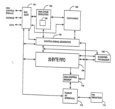
Referring to Fig. 2, DMA controller 52 includes DMA
cycle execution circuit 100, bus control circuit 101,
control signal generator circuit 102, look ahead circuit
103, first in, first out (FIF0) register circuit 104, FIF0
register backup circuit 108, DMA control backup circuit 110,
planar I/0 interface circuit 112, program/input/output (PI0~
register circuit 114 and error detection circuit 115. The
combination of cycle execution circuit 100, control signal
generator circuit 102, look ahead circuit 103 and DMA backup
controller 110 function as DMA control circuitry.
DMA cycle execution circuit 100, which includes DMA
control state machine 120, functions as the overall
controller of DMA controller 52. I.e., DMA cycle execution
circuit 100 orchestrates the operation of DMA controller 52
by providing high level control information. DMA cycle
execution circuit 100 provides control information to
control signal generator circuit 102 and receives count
information from control signal generator circuit 102. DMA
cycle execution circuit 100 also provides information to and
receives information from look ahead circuit 103 and DMA
control backup circuit 110. DMA cycle execution circuit 100
also provides, via bus control circuit 101, DMA control
signals to and receives DMA control signals from the control
information path between memory controller 50, DMA
controller 52 and bus interface unit 54 of base portion 22.
Bus control circuit 101 functions as the interface
between DMA controller 52 and any circuits which communicate
with DMA controller 52. Bus control circuit 101 includes
the circuitry which is necessary for receiving external
BC9-91-079 9 ~ 3 g ~
signals and providing these signals to the appropriate
circuit of DMA controller 52. Bus control circuit 101 also
includes the necessary logic to transmit signals which are
generated by circui-ts of DMA controller 52.
Control signal generator circui-t 102 is the functional,
basic controller of DMA controller 52. I.e., control signal
generator 102 generates individual control signals based
upon the high level control information which is received
from DMA cycle execu-tion circuit 100. Control signal
generator circuit 102 provides information to and receives
information from FIF0 register circuit 104 as well as look
ahead circuit 103. Control signal generator circuit 102
also provides information to and receives information from
DMA control backup circuit 110. Control signal generator
circuit 102 also provides, via bus control circuit 101,
address signals to the address information path between
memory controller 50, DMA controller 52 and bus interface
unit 54 of base portion 22.
Look ahead circuit 103 performs a dynamic bus sizing
function. Look ahead circuit 103 generates control
information for a plurality of bus sizes (e.g., 8-bit,
16-bit and 32-bit wide buses) as soon as a bus cycle begins.
The control information includes input variables for state
machine 120 of DMA cycle execution circuit 100 as well as
byte enable signals, FIF0 control signals, address control
signals, count control signals and data control signals for
control signal generator circuit 102. By continuously
generating this information, look ahead circuit 103 allows
DMA controller to switch on the fly between different bus
sizes during every bus cycle. By generating the control
information in parallel, look ahead circuit 103 allows DMA
controller 52 to run memory or I/O transfers with no
additional wait states. E.g., a memory packet transfer
requires only six clock cycles and an I/0 or single memory
transfer re~uires only three clock cycles.
Look ahead circuit 103 also generates the control
information necessary for the initial transfer of a bus
cycle. Accordingly, look ahead circuit 103 also allows DMA
controller to perform zero wait state packet transfers to
system memory 16, 17.
BC9-91-079 10 2 0 7 ~
FIF0 reglster circuit 104, which is a 20-byte FIF0,
performs a holding function for DMA controller 52. FIF0
register clrcuit 104 allows for accumulating data so that
the memory portion of a transfer can be aligned on a 16-byte
packet boundary, thus allowing memory transfers to occur in
16-byte packet transfers. Packet transfers allow one
address to be provided for a plurality of data bytes (e.g.,
one address for four 32-bit words). By providing a 20-byte
FIF0, the chances of finding a packet boundary of a 16-byte
packet are increased. FIF0 register circuit 104, via bus
control circuit 101, provides data information to and
receives data information from the data information path
between DMA controller 52, bus interface unit 54 and
buffer/ECC circuit 56. FIF0 register circuit 104 also
provides data information to and receives data information
from FIF0 backup circuit 108 as well as providing control
information to DMA control backup circuit 110.
FIF0 register circuit 104 is also used to load
subsystem control blocks (SCB s) of data; each SCB is 16
bytes in length. The SCB s are stored in DMA control backup
circuit 110 when DMA controller 52 is functioning in the bus
master mode. Accordingly, DMA controller 52 can configure a
DMA channel in one 16 byte packet transfer compared to
programming a DMA channel using the PI0 interface and
individual I/0 cycles. By using DMA controller 52 to
configure the DMA channels, processor 30 is not required.
FIF0 backup circuit 108 performs a channel backup
function for DMA controller 52. FIF0 backup circuit 108 is
an eight channel backup circuit; each channel being capable
of storing 20 bytes of data as well as 29 FIF0 state control
bits. By providing a backup memory which is the same width
as FIF0 register circuit 104, all of the information which
is stored in FIF0 register circuit 104 at any given time
can be backed up and stored in a single memory clock cycle.
By using FIF0 backup circuit 108, DMA controller 52 has the
ability to store information between DMA grant cycles. This
information is called residual information. Accordingly,
when a particular DMA channel regains control of I/0 bus 18,
clock cycles are saved as it is not necessary to retrieve
the information from memory. The information is transferred
BC9-91-079 11 2 ~
between FI~O backup circ~lit 1()8 and FIFO register circuit
104 in parallel.
DMA control backup circuit llO is an 8-channel storage
device which stores contro:l information provided by control
signal generator circuit :L02 and provides control
information to con-trol signal generator circuit 102. DMA
control backup circuit 110 provides backup programming
information to and receives backup programming information
from planar I/O interface circuit 112 during PIO operations.
DMA control backup circuit 110 also receives control
information from and provides control information to bus
controller 101 via FIFO register circuit 104 during SCB
fetches.
Planar I/O interface circuit 112 controls transferring
and storing information in PIO registers 114 as well as DMA
control backup 110. Planar I/O interface circuit provides
PIO programming information to and receives PIO programming
information from PIO registers 114.
PIO registers 114 store program information which is
used during the operation of DMA controller 52. PIO
registers include eight channels, corresponding to the eight
channels of DMA controller 52. Each channel stores control
information for a corresponding channel of DMA controller
52.
Error detection circuit 115 monitors possible error
conditions and generates DMA error indication information
based upon these conditions. Error detection circuit 115
receives information from DMA control backup circuit 110 and
DMA state machine 120 and provides the error indication
information to bus controller 101.
Referring to Fig. 3, bus control circuit 101 receives
and provides a 32-bit data signal (DO-31), a 30 bit address
signal (A2-31) and a four bit byte enable signal (BEO-3) as
well as receiving a data ready signal (RDY) and a burst data
ready signal (BRDY). Bus control circuit also receives DMA
control signals, DMAACK, TIMEOUT, BURST and ACT CHNL(0-2).
The DMAACK signal is a DMA acknowledge signal which
indicates that DMA controller 52 has control of bus 18, the
TIMEOUT signal is an error indication signal which indicates
that DMA controller 52 should terminate transferring
BC9-91-079 1~ 2 ~ ri ~
information, the BURST signal is provided by external
devices to indicate that they are capable of sending or
receiving more than one data transfer in a row, and the ACT
CHNL(0-2) signal is a DMA channel active indication signal
which indicates which channel of DMA controller 52 is
active. Bus control circuit 101 transmits a burst last
signal (BLAST), which is provided by DMA controller 52 to
indicate that it intends to provide a packet transfer, an
address strobe signal (ADS), which indicates when to sample
address and control information, a write/read signal (W/R),
which indicates whether a read or a write operation is to
take place and a memory I/0 signal (M/I0), which indicates
whether a memory or I/O device is being accessed. Bus
control circuit 101 also transmits DMA control signals
MEMFLUSH, TC and DMAACTIVE. The MEMFLUSH signal indicates
that remaining operations for a channel of DMA controller 52
are only memory write operations. The TC signal is a
terminal count signal which is provided at the end of the
last I/0 cycle. The DMAACTIVE signal is a DMA active signal
which stays active as long as DMA controller 52 is active
(i.e., performing a transfer). Bus control circuit 101 also
receives a bus size valid signal (BSV) and bus size
indication signals (BS16, BS32). Information which is
received by bus control circuit 101 is provided to DMA
control state machine 120, DMA control backup circuit 110,
FIF0 backup memory 108 and FIF0 register circuit 104.
Information is also provided to and received from look ahead
circuit 103 and control signal generator circuit 102.
Control signal generator circuit 102 includes SCB fetch
controller 122; DMA transfer controller 123 which includes
mode controller 124, first address generator 126, second
address generator 128, transfer count controller 130, and
byte enable generator 132; and, FIF0 controller 134. SCB
fetch controller 122 and FIF0 controller 134 are control
circuits of control signal generator circuit 102. Mode
controller 124, first address generator 126, second address
generator 128, transfer count controller 130 and byte enable
generator 132 are also control circuits of control signal
generator circuit 102.
SCB fetch controller 122 determines whether an SCB
transfer should transpire. If so, then SCB fetch controller
BC9-91-079 13 ~ d, ~3 ~ ~
122 initiates and completes an SCB transfer to DMA control
backup circuit 110 via FIFO register circuit 104. Once the
SCB transfer is completed, SCB fetch con-troller 122 provides
a control signal to DMA con-tro] state machine which
indicates that DMA transfers may be initiated. Once DMA
controller 52 has been configured for a transfer, it is not
necessary to reconfigure DMA controller 52 until the
transfer is completed. SCB fetch controller 122 also allows
chaining of a plurality of data blocks, thus allowing
noncontiguous data blocks of information to be chained
together.
DMA transfer controller 123 generates DMA transfer
signals which are necessary to effectuate a DMA transfer.
DMA transfer controller 123 generates these signals based
upon control signals which are received from DMA control
state machine. More specifically, the control circuits of
DMA transfer controller 123 generate these DMA transfer
signals
Mode controller 124 of DMA transfer controller 123
interprets mode information which is stored in DMA control
backup circuit 110 and provides control information to DMA
control state machine 120 of DMA cycle execution circuit
100 based upon the mode information. Examples of different
modes in which DMA controller 52 may function include I/O to
memory transfers, memory to I/O transfers, and memory to
memory transfers; for each of these modes, different
operations may be performed by control circuits of control
signal generator circuit ]02 under control of DMA control
state machine 120. Mode controller 124 also sets forth
other aspects of a DMA transfer, e.g., whether FIFO register
circuit 104 is required and thus should be enabled for a
particular DMA transfer.
First address generator 126 and second address
generator 128 of DMA transfer controller 123 generate
address signals which represent a source address and a
destination address for a DMA transfer. If the transfer is
to or from an I/O device, then the first address generator
remains constant. If the transfer is a memory to memory
transfer, then both address signals are generated
continuously during the transfer. First address generator
126 and second address generator 128 generate the address
BC9-91-079 14 ~ 3 ~ ~
signals under control of DMA control state machine 120.
First address generator 126 may generate either the source
or the destination address; second address generator 128
generates the address which was not generated by first
address generator 126.
Transfer count controller 130 generates transfer
control information based upon the size of the block of
information which is transferred during a particular
transfer. When a transfer is initiated, transfer count
controller 130 is loaded with control information indicating
the size of the block of information which is to be
transferred. This information is decremented with each byte
that is transferred; when the transfer count equals zero,
transfer count controller 130 provides a transfer count
signal to DMA control state machine 120 which indicates that
the transfer is complete.
Byte enable generator 132 generates the necessary byte
enable signals at the beginning of each cycle, thus
indicating which bytes to transfer during a particular DMA
transfer. Byte enable generator 132 also generates byte
enable signals which are provided to FIF0 controller 134,
thus allowing FIF0 controller 134 to determine in which
locations of FIF0 register circuit 104 valid data
information is stored.
FIF0 controller 134 includes circuitry which generates
FIF0 control signals which are used to move bytes of data
information into the stack of FIF0 register circuit 104.
The control signals also produce a count of how many bytes
of information have been loaded into FIF0 register circuit
104. This count information is used to determine how full
FIF0 register circuit 104 is to determine when to transition
between states. FIF0 control information which is generated
by FIF0 controller 134 is also provided to FIF0 backup
memory 108.
Look ahead circuit 103 includes initial value circuit
140, size-8 look ahead circuit 142, size-16 look ahead
circuit 144, size-32 look ahead circuit 146 which all
provide control information to multiplexer circuit 148 as
well as bus size select circuit 150 which provides a control
input signal to multiplexer circuit 148. Initial value
circuit 140 generates the control information necessary for
BC9-91-()79 ]~ 2 `~ 3 g 1
the initial transfer of a bus cycle; in generating the
initial transfer information, initial value circuit 140
assumes the widest transfer size, i.e., 32-bit wide
transfers. Size-8 look ahead circuit 142, size-16 look
ahead circuit 144 and size-32 look ahead circuit 146
generate in parallel the sets of control information
necessary for transfers of information based on the
respective bus size. Multiplexer circuit 148 passes one of
these sets of control information as a next set of control
information based upon the present cycle s bus size under
control of bus size select circuit 150. Bus size select
circuit 150 receives the BSV, B~32 and BS16 signals, which
indicate the bus size necessary for data information
transfer, from bus controller 101 and selects the
appropriate control information to pass for the next cycle
based upon these signals. Because control information for
each bus size is generated in parallel, as soon as a bus
size is selected, the control information for this bus size
may immediately be provided to control signal generator
circuit 102 for generating the control information for the
next cycle, thus decreasing latency between consecutive DMA
bus cycles. Bus sizes may vary because expansion devices 19
transfer information in different bus sizes. Accordingly,
DMA controller 52 may transfer information at a first bus
size during a first cycle and at a second bus size during a
second subsequent cycle. Thus, DMA controller 52 is capable
of transferring data between system devices without any
prior knowledge of their respectlve bus widths and with no
reduction in system performance.
The output signal of multiplexer circuit 148 is
provided to the control circuits of control signal generator
circuit 102 and to DMA control state machine 120. These
control circuits also provide and receive signals from DMA
control state machine 120 and provide control signals to
size-8 look ahead circuit 142, size-16 look ahead circuit
144 and size-32 look ahead circuit 146.
Error detection circuit 115 monitors information from
DMA control backup circuit 110 and state machine 120 and
generates a DMA error signal (DMA ABORT) which indicates
that a DMA error has occurred. The DMA ABORT signal is
BC9-91-079 16 ~ 3 ~ ~
provided to bus control circuit 101 which provides this
signal to CACP 53.
Referring to Figs. 3 and 4, FIF0 portion of DMA
controller 52 includes FIF0 buffer 104, FIF0 backup memory
108 and FIF0 controller 134 of control signal generator
circuit 102. FIF0 controller 134 of control signal
generator circuit 102 provides control signals to FIFO
buffer 104 and FIF0 backup memory 108. FIF0 backup memory
108 provides data information to FIF0 buffer 104 in parallel
and receives data information from FIF0 buffer 104 in
parallel. Accordingly, data information can be transferred
between FIF0 backup memory 108 and FIF0 buffer 104 in a
single memory cycle. Transfers of data occur under control
of FIF0 controller 134.
FIF0 buffer circuit 104 includes input steering
multiplexers 202, a plurality of buffer cells (e.g., final
stage cells 204, intermediate stage cells 206 and initial
stage cells 208) and output steering multiplexers 210. The
buffer cells are arranged in rows (i.e., banks) and columns,
each row consisting of a final stage cell 204, one or more
intermediate stage cells 206, and an initial stage cell 208
and each column consisting of a plurality of final stage
cells 204, intermediate stage cells 206 or initial stage
cells 208. For a 20-byte FIF0 register circuit, FIF0
register circuit 104 includes three columns of intermediate
cells as well as four rows of cells.
Input steering multiplexers 202 receive the 32-bit data
signal from bus controller 101. Each multiplexer 202
provides eight bits of the data signal to a respective row
of buffer cells, i.e., a respective final stage cell 204, a
respective intermediate stage cell 206 and a respective
initial stage cell 208 in parallel under control of FIF0
controller 134. Final stage cells 204, intermediate stage
cells 206 and initial stage cells 208 also receive data
information in parallel from FIF0 backup memory 108. Each
final stage cell 204 provides a data information signal to a
respective intermediate stage cell 206; each intermediate
stage cell 206 provides a data information signal to another
intermediate stage cell 206 or a respective initial stage
cell 208. Initial stage cells 208 provide data information
signals in parallel to output steering multiplexers 210
BC9-91-079 17 2 & 7 ~ 3 ~ ~
which combine the signals which are received from initial
stage cells 208 to provide a 32-bit data signal to bus
controller 101.
Each final stage cell 204 includes final stage cell
multiplexer 212 and final stage cell control circuit 213.
Each intermediate stage cell 206 includes intermediate stage
cell multiplexer 214 and intermediate stage cell control
circuit 215. Each initial stage cell includes initial stage
cell multiplexer 216 and initial stage cell control circuit
217. The only difference between final stage cell
multiplexer 212 and intermediate stage cell multiplexer 214
or initial stage cell multiplexer 216 is final stage cell
multiplexer is a 2:1 mux whereas intermediate stage cell
multiplexer 214 and initial stage cell multiplexer 216 are
3:1 muxes. Cell multiplexers 212, 214 and 216 all receive a
data input signal from backup memory 108. All of the
multiplexers 212, 214, 216 of a row of buffer cells also
receive in parallel a data input signal from a respective
input steering multiplexer 202. Intermediate cell
multiplexer 214 also receives a data information signal from
final stage control circuit 213; initial stage multiplexer
216 receives a data information signal from intermediate
stage control circuit 215. Cell multiplexers 212, 214 and
216 select which input signal to pass under control of FIFO
controller 134.
FIFO controller 134 includes read pointer 220, write
pointer 222, data in steer controller 226 and data out steer
controller 224 as well as backup memory control circuit 228
and FIFO control signal register circuit 230. Read pointer
220 receives a read strobe signal (RD STR) and generates
read pointer signals, which are provided to data out steer
controller 224 and FIFO backup memory 108. Write pointer
222 receives a write strobe signal (WR STR) and generates
write pointer signals, which are provided to data in steer
controller 226 and FIFO backup memory 108. Data out steer
controller 224 and data in steer controller 226 also receive
a FIFO byte enable signal (FIFOBE), a transfer count signal
(XFERCNT), and a parallel write strobe signal (P WR STR).
Data in steer controller 226 controls input steering
multiplexers 202 based upon these signals and data out steer
multiplexer 224 controls output steering multiplexers 210
BC9-91-079 lf3 2 ~ ~ ~ 3 J .i
based upon these signals. Backup memory control circuit 228
receives a 3-bit active channel i.ndication signal (ACT
CHNL(0-2)), a memory read or write signal (RAM W/R) and a
memory clock signal (RAM CLK). FIFO control signal register
circuit 230 receives a p].urality of FIFO control signals and
provides control signals to FIFO register circuit 104.
Referring to Fig. 5, intermediate stage cell control
circuit 215 includes byte valid control circuit 250, byte
valid flip flop 252, cell clock control circuit 254 and cell
data register 256. Byte valid control circuit 250
determines whether a byte is to be stored by intermediate
stage cell 206 based upon a plurality of control signals.
Byte valid control circuit 250 indicates that a byte of data
should be valid following the next clock cycle. Byte valid
flip flop 252 synchronizes the output of byte valid control
circuit 250 with the CLOCK signal, and then provides the
BYTE VALID signal to cell clock control circuit 254, byte
valid control circuit 250 and other neighboring cell control
circuits 250. Cell clock control circuit 254 synchronizes
the BYTE VALID signal with an appropriate strobe signal
based upon the type of operation which is being performed by
the buffer cell. The synchronized BYTE VALID signal is the
clock gating input to flip flop 256 which synchronizes the
FIFO data output signal based upon the input from
multiplexer 214.
Byte valid control circuit 250 receives the WR STR and
RD STR signals as well as byte valid signals (BV(I-l), BV(I)
and BV(I+l)). BV(I-l) is the BYTE VALID signal from a
previous respective stage of FIFO register circuit 104
(i.e., the BYTE VALID signal from final stage cell 204);
BV(I+l) is the BYTE VALID signal from a subsequent
respective stage of FIFO register circuit 104 (i.e., the
BYTE VALID signal from initial stage 208 or from a
subsequent intermediate state 206). Byte valid control
circuit 250 also receives byte control signals backup byte
valid ~BACKUP BYTE VALID), which is the BYTE VALID signal
which corresponds the data information which is stored in
FIFO backup memory 108, FIFO write not read (FIFO WNR),
which indicated whether to write data information to or
read data information from FIFO register circuit 104, FIFO
flush (FIFOFLUSH), which indicates when to clear the buffer
BCg-91-079 19 ~ 3l~
cells after the information in the cells is backed up in
FIFO backup memory 108, and a system reset signal (RESET),
which resets all of the information of the FIFO circuits.
Byte valid control circuit 250 provides a byte valid signal
to flip flop 252 which is clocked by a cell clock signal
(CLOCK). Flip flop 252 prov:ides the clocked BYTE VALID
signal to cell clock control circuit 254.
Cell clock control circuit 254 also receives the cell
clock signals RD STR, WR STR, P RD STR and P WR STR as well
as the CLOCK signal. Cell c].ock control circuit 254
provides a clocked BYTE VALID signal to the clock input
terminal of flip flop 256, which receives the data output
signal from intermediate stage cell multiplexer 214.
Referring to Figs. 1 - 3, 6 and 9, in operation, CACP
53 performs an arbitration function under control of
arbitration control state machine 300. Arbitration control
state machine 300 actually includes both CACP state machine
534 and LACP state machine 520. During operation of
computer system 10, one of these state machines is selected
based upon the state of a mode indication signal (CACP
MODE). However, the interaction between arbitration state
machine 300, DMA control state machine 120 and refresh
control state machine 301 remains the same regardless of
whether arbitration state machine 300 is functioning in the
CACP mode or the LACP mode. If during arbitration, DMA
controller 52 wins ownership of bus 18, then the DMAACK
signal is activated by CACP 53 and control shifts to
supervisory state machine 302 of DMA control state machine
120, which also includes execution state machine 304.
Supervisory state machine 302 performs initialization
functions after which control is provided to execution state
machine 304 as indicated by an active DMAGO signal.
Execution state machine 304 controls the actual transfer of
direct memory access information. After a transfer is
complete, as indicated by an active DONE signal, control is
transferred back to supervisory state machine 302, which
performs completion functions, after which control is passed
back to arbitration state machine 300, as indicated by an
inactive DMAACK signal and another arbitration cycle is
initiated. If during arbitration, a refresh operation is to
be performed, as indicated by an active REF ACK signal, then
BC9-91-079 2 n
control is passed to refresh control state machine 301.
After the refresh operation is complete, as indicated by an
active REF DONE signal, then control is passed back to
arbitration state machine 300.
Referring to Fig. 7, supervisory state machine 302
cycles in idle state 350 until the DMAACK signal is
activated. When the DMAACK signal is received, control is
passed to wait state 352 which activates the DMA ACTIVE
signal and allows control signals to settle prior to
transfer to read memory state 354. Read memory state 354
fetches and reads DMA and SCB control information from DMA
control backup circuit 110 and provides this information to
control signal generator circuit 102. More specifically,
the control information is loaded into mode controller 124,
address generators 126, 128, transfer count controller 130
and byte enable generator 132. Additionally, FIFO
information which is stored in FIFO backup memory 108 is
loaded into FIFO register circuit 104 and FIFO controller
134. During read memory state 354, information which is
stored in SCB controller 122 determines what type of
transfer information is loaded into control signal generator
circuit 102, e.g., whether a DMA transfer is to occur or
whether an SCB transfer is to occur.
For a DMA transfer, control is passed to wait state 358
which activates the DMAGO signal. When the DMAGO signal is
activated, control is passed to DMA execution state 360, via
which control is passed to execution state machine 304.
When DMA execution state machine 304 completes the transfer,
the DONE signal is activated, control is returned to
supervisory state machine 302, and control is passed to
write state 362. Write state 362 stores the control
information which is in the control circuits of control
signal generator circuit 102 in DMA control backup circuit
110. Also, in write state 362, data information is
transferred from FIFO register circuit 104 to FIFO backup
memory 108. Additionally, in write state 362, the DMA
ACTIVE signal is set inactive, which causes arbitration
circuit 53 to set the DMAACK signal inactive and control is
returned to idle state 350. Control remains with idle state
350 until the DMAACK signal is again activated by CACP 53.
sC9-91-079 21 2 ~
For an SCB tran.sfer, the control information, including
an SCB pointer, is loaded from DMA control backup circuit
110 into control signal generator circuit 102 during initial
memory read state 354. Control is passed from read state
354 to SCB execution state 366. During SCB execution state
366, SCB programming information is retrieved from system
memory. SCB fetch controller 122 provides a fetch count
which is used in retrleving the SCB information. SCB
execution state 366 uses look ahead circuit 103 to generate
pertinent control information based upon all possible bus
sizes so that the SCB information may be retrieved as soon
as the BSV signal goes active. The SCB information is
placed temporarily in FIF0 register circuit 104. After
retrieving the information from SCB controller 122, control
is passed to write state 362, where the SCB programming
information is stored in DMA control backup circuit 110.
After the SCB information is stored in DMA control backup
circuit 110, control passes to memory read state 354 to
initiate a DMA transfer. The SCB information which is
retrieved is 16-bytes wide: four bytes indicating the mode
of a transfer; four bytes indicating a first address (the
first address is the I/0 address for transfers which use an
I/0 device 19 or is the first memory address for memory to
memory transfers); four bytes indicating a second address;
and four bytes indicating a transfer count.
Supervisory state machine 302 is also capable of
controlling data chaining operations. A data chaining
operation is indicated by part of the mode information of
the initial 16-byte SCB which is loaded during SCB execution
state 366. Direct memory access transfers require data
information to be stored in contiguous memory locations.
Accordingly, if information is stored in noncontiguous
blocks, then data chaining is used to effectuate a scatter
or gather direct memory access transfer.
For data chaining operations, supervisory state machine
302 retrieves indirect list (ILIST) information in addition
to the initial 16-byte SCB. The ILIST is a group of 8-byte
ILIST SCB s; each ILIST SCB includes a four byte second
address and a four byte transfer count. When a data
chaining operation is indicated in the mode information of
the SCB which is retrieved during SCB execution state 366,
BC9~-91-079 ~2 2 ~ ~ ~ 3 ~
then after this SCB is written to memory during write state
362, control is transferred to SCB ILIST memory read state
368 during which the control information necessary to
retrieve the ILIST information is loaded into control signal
generator circuit 102. After this information is loaded,
control is transferred to ILIST fetch state 370 during which
the ILIST information is retrieved from system memory and
placed temporarily in FIF0 register circuit 104.
Control is then passed to write state 372 where the
ILIST information is written to DMA control backup circuit
110. Control is then passed to write state 374 in which the
ILIST pointer and the ILIST counter are stored in DMA
control backup circuit 110. The ILIST pointer and counter
are used to track which ILIST SCB of a particular data chain
is to be used for the next DMA transfer. Control is then
returned to idle state 350 if no DMA transfer is to occur
or, if DMA controller 52 still has ownership of bus 18,
control is passed to memory read state 354 to initiate a DMA
transfer.
ln addition to the operation states of supervisory
state machine 302, supervisory state machine 302 also
includes error state 376. Control transfers from certain
operation states, e.g., memory read state 354, to error
state 376 upon certain error conditions. A timeout
condition is an example of an error state. Error state 376
performs certain completion tasks prior to returning to idle
state 350, thus allowing DMA controller 52 to exit
gracefully from error conditions.
Referring to Fig. 8, DMA execution state machine 304 is
organized in two portions, to the right of idle state 400 is
a FIF0 enabled portion and to the left of idle state 400 is
a FIF0 disabled portion. During operation of both portions,
FIF0 register circuit 104 is used as a holding mechanism.
However, when operation of DMA execution state machine 304
is via the FIF0 enabled portion, FIF0 register circuit is
filled with data information, e.g., when FIF0 register
circuit 104 is used with burst transfers or to optimize
transfers between I/0 devices l9 and the system memory. The
operation of the different states of DMA execution state
machine 304 also depends on the mode of the DMA transfer.
Prior to passing control to execution state machine
BC9-91-079 23 ~rJ~3~l
304, it remains in idle state 400. As long as the DMAGO
signal remains inactive, control remains with idle state
400. When the DMAGO signal goes active, then control passes
to either the FIFO enabled portion of DMA execution state
machine 304 or to the FIFO disabled portion of DMA execution
state machine 304 depending on the state of the FIFOEN
signal. When the DMAGO signal is active, in conjunction
with an active FIFOEN signal, control is passed to bus size
valid read state 402.
For an I/O to memory transfer, as indicated by the mode
information which is stored in mode controller 124, data
information is read from the I/O device at the beginning of
the cycle. While waiting for the BSV signal to go active,
look ahead circuits 142, 144, 146 of look ahead circuit 103
are receiving information from the control circuits of
control signal generator circuit 102 and generating control
information which will be provided to the control circuits
of control signal generator circuit 102 and execution state
machine 304 based upon the width of the expansion devices as
indicated by the BS16 and BS32 signals. When the BSV signal
goes active, the control circuits of control signal
generator circuit 102 are updated and control is passed to
ready read state 404.
Control remains in ready read state 404 until the RDY
signal goes active. When the RDY signal goes active, data
information is latched from bus 18 into bus controller 101.
One clock cycle later, this data information is provided to
FIFO register circuit 104 and bus controller 101 is ready to
latch more data information. During ready read state 404,
the look ahead signals which are being generated by look
ahead circuit 103 are monitored to determine whether any
more data information is to be read. If more data is to be
read, then control is returned to BSV read state 402 and the
process is repeated. If there is no more data information
to be read, then, for an I/O to memory transfer, control is
passed to bus size valid write state 406.
During bus size valid write state 406, control
information regarding the bus size is provided to the
control information path of base portion 22. Bus size valid
write state 406 assumes a 32-bit wide path and positions
data from FIFO register circuit 104 to be provided to the
BC9-91-079 2~
data information path of base portion 22 in 32-bit segments
unless FIFO register circul-t 104 contains less than four
bytes or the memory address is not a]igned on a double word
boundary. When the BSV signal goes active, control is
passed to ready write state 408; when the RDY signal goes
active, the data information is written out of FIFO register
circuit 104 to memory in a burs-t. During ready write state
408, the look ahead signals which are being generated by
look ahead circuit 103 are monitored to determine whether
any more data information is to be written. If more data is
to be wri.tten, then control is returned to BSV write state
406 and the process is repeated. Data information is
written until FIFO register circuit 104 does not contain
enough data to effectuate a transfer.
If after the data information is written from FIFO
register circuit 104 and DMA controller 52 still owns bus
18, then control is passed to bus size valid state 402 and
another read cycle is initiated. If the data transfer for
the channel is complete, as indicated by an active CNL DONE
signal, then control is passed to execution complete state
410. At execution complete state 410, the contents of the
control circuits of control signal generator 102 are
updated, the DONE signal is activated and control is passed
back to idle state 400, and thus back to supervisory state
machine 302. If more data is to be read from the I/O
device, then control is returned to BSV write state 406 and
the process is repeated.
For a memory to I/O transfer, which is indicated by the
mode information which is stored in mode controller 124, the
transfer is similar to that of an I/O to memory transfer.
Executory state machine 304 uses the FIFO enabled portion
and transfers control to bus size valid read state 402.
Data information is read from the memory device at the
beginning of the cycle. While waiting for the BSV signal to
go active, look ahead circuits 142, 144, 146 of look ahead
circuit 103 are receiving information from the control
circuits of control signal generator circuit 102 and
generating control information which will be provided to the
control circuits of control signal generator circuit 102 and
execution state machine 304 based upon the width of the
BC9-91-079 25 2 ~ ~ ~ 3~ ~
memory device as indicated by the BS16 and BS32 signals.
When the BSV signal goes active, the control circuits of
control signal generator circuit 102 are updated and control
is passed to ready read state 404. Control cycles between
bus size valid read state 402 and ready read state 404 until
FIFO register circuit 104 is filled with data information.
When the RDY signal goes active in conjunction with an
active BURST signal, data information is read from memory
and control is passed to bus size valid write state 406.
During bus size valid write state 406, for a memory to I/0
transfer, control information is generated by look ahead
circuit 103 while waiting for bus size information from I/0
bus 18. Accordingly, when the BSV signal goes active,
control can be passed to ready write state 408 and the data
information which is held in FIF0 register circuit 104 can
be written to the I/0 device 19. Data information is
written to the I/0 device 19 until FIF0 register circuit 104
is empty. FIF0 register circuit 104 is empty if there is
not enough data remaining in FIF0 register circuit 104 to
complete an I/0 transfer. At this point control is either
passed to bus size valid read state 402 or to execution
completion state 410 as with an I/0 to memory transfer.
If during ready read state 404, when the RDY signal
goes active, the BURST signal is inactive, indicating that
the I/0 device 19 may receive only one transfer (e.g.,
because I/0 device 19 is a non-bursting device), then
control is passed to bus size valid write state 412. During
bus size valid write state 412, the information necessary to
transfer the data information is generated by look ahead
circuit 103 so that when the BSV signal is activated,
control may be transferred to ready write state 414. When
the RDY signal goes active, the data information is
transferred to the I/0 device 19 and control is passed to
adjust count and address state 416. During adjust count and
address state 416, the count and address which is stored in
DMA transfer controller 123 are adjusted to track the
residual data information which is in FIF0 register circuit
104, and control is passed to execution completion state
410.
BC9-91-079 26 2 ~
For a memory to I/O transfer, when control is passed to
executory state machine 304, FIFO register circuit 104 may
have data information which was received during a previous
transfer cycle. There may be information in FIFO register
circuit 104, for example, because the I/O device 19 is a
non-bursting device which cannot receive the entire contents
of FIFO register circuit 104 in a single transfer cycle.
Accordingly, during a subsequent transfer cycle, it is not
necessary to reload FIFO register circuit 104 and control
may transfer directly from idle state 400 to bus size valid
write state 406.
If, when control is passed to idle state 400 of
execution state machine 304, the DMAGO signal is active
while either the FIFOEN signal is inactive, indicating that
FIFO register circuit 104 is not enabled or the MEMVER
signal is active, indicating that a memory verify operation
is enabled then the FIFO disabled portion of execution state
machine 304 is used and control is passed to bus size valid
read state 418. During bus size valid state 418, look ahead
circuit 103 generates the control information necessary to
effectuate a transfer When the BSV signal goes active,
this control information is loaded into the control circuits
of control signal generator circuit 102 and control is
passed to ready read state 420. Control remains with ready
read state 420 while the RDY signal remains inactive. When
the RDY signal goes active then, if the MEMVER signal is
active, control is transferred to execution complete state
410. The memory verify operation is used to test transfer
cycles without testing data integrity.
If the MEMVER signal is inactive, control is passed to
bus size valid write state 422. During bus size valid write
state 422, look ahead circuit 103 generates the control
information necessary to write the data information which is
held in FIFO register circuit 104. When the BSV signal goes
active, then control is passed to ready write state 424.
While the RDY signal is inactive, control remains with ready
write state 424. If,when the RDY signal goes active, the
BURST signal is active and at least four bytes remain in
E'IFO register circuit 104, then control is passed back to
bus size valid write state 422 and more data information is
written. If the CNL DONE signal is active in conjunction
BC9-91-079 27 2 J ~
with the NO RESIDUAL signal then control is passed to
execution complete state 410. If the CNL DONE signal is
active in conjunction with the RESIDUAL signal, then control
is passed to adjust count state 416. The address and count
information of DMA transfer controller 123 is adjusted and
control is passed to execu-tion complete state 410.
In addition to the transitions that are shown, every
state which monitors the RDY signal, e.g., ready read state
404, has a path to complete state 410 when the TIMEOUT
signal is active. In this way, when an error condition
occurs, a direct path is provided via which error state 376
of supervisory state machine 302 may be reached.
Referring again to Figs. 1, 3 and 4, in operation, when
DMA controller 52 initiates any type of transfer,
information which is to be transferred is read from a
device, e.g., system memory 16, 17, and written into FIFO
register circuit 104. The information which is held in FIFO
register circuit 104 is then read from FIFO register circuit
104 and written to another device, e.g., an I/O device 19.
Thus, a system read produces a FIFO write and a FIFO read
produces a system write. Data information which is held in
FIFO register circuit 104 is tracked via a read pointer and
a write pointer which are generated by read pointer circuit
220 and write pointer circuit 222. The read pointer
identifies where the first byte of data which is held in
FIFO register circuit 104 is located, i.e., in which cell
this information is held. The write pointer identifies the
location where the next byte of data is written in FIFO
register circuit 104. For the first byte of data which is
written to FIFO register circuit 104, these two pointers are
the same. For each subsequent byte of data information
which is written to FIFO register circuit 104, the write
pointer is incremented; the read pointer remains the same.
In this way, it is possible to determine to which cell to
write the next byte of data information. In addition to
incrementing the write pointer, when data is written into a
cell, the BYTE VALID signal for that cell is set active,
thus indicating that valid data information is stored in the
cell. When data information is read from FIFO register
circuit 104, the read pointer is incremented with each byte
of data which is read. The read and write pointers are
BC9-91-079 28 ~7 ~33~1
stored in FIFo backup memory 108 along with the data
information from the buffer cells.
Supervisory state machine 302 also determines whether a
transfer is an initial transfer cycle, i.e., the first
transfer which uses FIF0 register circuit 104. If a
transfer is an initial transfer, then data information is
read directly from a source device rather than loading data
information from FIF0 backup memory 108.
If a transfer is not an initial -transfer, as determined
by supervisory state machine 302, -then register circuit 104
is loaded from FIF0 backup memory 108 prior to reading
information from the source device. The BYTE VALID signals,
which are stored along with the data information when FIF0
register circuit 104 is backed up, are used to determine
which buffer cells have data information stored in them
after the data information is retrieved by FIF0 register
circuit 104.
For the first write to FIF0 register circuit 104, the
first byte of data information is written to initial stage
cell 208a. The next byte of data is written to initial
stage cell 208b and so on. After all four initial stage
cells are written to, then the next byte of data information
is written to intermediate stage cell 206a. Data may be
written until all of the buffer cells of FIF0 register
circuit 104 contain data information, thus 20-bytes of data
may be written to FIF0 register circuit 104 without reading
any information from it. With each byte that is written,
the write pointer is incremented so that when the contents
of FIF0 register circuit 104 are retrieved from FIF0 backup
memory 108, data can be written to the next available cell.
Because the data information is written directly to initial
stage cells 208 (i.e., data information is loaded into the
front end of the FIF0 register), this data information is
immediately available to be read from FIF0 register circuit
104. Accordingly, a FIF0 write and a FIF0 read can occur in
subsequent cycles.
The read pointer is used to track where the initial
read should occur, e.g., for the initial read, the read
pointer points to initial stage cell 208a. With each read,
the read pointer is incremented. Accordingly, if during the
BC9-91--~79 29 ~J ~ 7 .~
initial cycle, -two bytes were read and then the contents of
FIF0 register circuit 104 were stored in FIF0 backup memory
108, then read pointer would point to initial stage cell
208c when FIF0 register circuit 104 is reloaded from FIF0
backup memory 108.
Data out steering controller 228 determines which
multiplexer of output steering multiplexers 210 pass which
bytes of data. For example, for an initial read,
multiplexer 210 passes the data information which is
received from initial stage cell 208a. For a read where
read pointer is pointing to initial stage cell 208c,
multiplexer 210 passes the data information which is
received from initial stage cell 208c.
Referring again to Fig. 5, byte valid control circuit
250 determines the state of the BYTE VALID signal, and thus
controls whether the information which is stored in a buffer
cell is interpreted as valid information. In this way, the
byte valid control circuits control shifting data
information across rows of FIF0 register circuit 104.
For an initial stage cell 208, when the BYTE VALID
signal is inactive and a write operation is performed, then
the next value of the BYTE VALID signal is active. When the
BYTE VALID signal is active and a write operation is
performed, then the next value of the BYTE VALID signal is
active. When the BYTE VALID signal is inactive and a read
operation is performed, then the next value of the BYTE
VALID signal is inactive. When the BYTE VALID signal is
active and a read operati.on is performed, then the next
value of the BYTE VALID signal is BV(I - 1).
For an intermediate stage cell 206, when the BYTE VALID
signal is inactive and a write operation is performed, then
the next value of the BYTE VALID signal is the BV(I + 1)
value. When the BYTE VALID signal is active and a write
operation is performed, then the next value of the BYTE
VALID signal is active. When the BYTE VALID signal is
inactive and a read operation is performed, then the next
value of the BYTE VALID signal is inactive. When the BYTE
VALID signal is active and a read operation is performed,
then the next value of the BYTE VALID signal is BV(I - 1).
For a final stage cell 204, when the BYTE VALID signal
is inactive and a write operation is performed, then the
BC9-91-079 30 ~d ~ 7 ~
next value of the BYTE VALID signal is BV(I + 1). When the
BYTE VALID signal is ac-tive and a write operation is
performed, then the next value of -the BYTE VALID signal is
active. When the BYTE VALID signal is inactive and a read
operation is performed, then the nex-t value of the BYTE
VALID signal is inactive. When the BYTE VALID signal is
active and a read operation is performed, then the next
value of the BYTE VALID signal is inactive.
Referring to Fig. 9, CACP circuit 53 includes soft
reguest arbiter portion 500, DMA channel selection portion
501, and system control portion 502. Soft request arbiter
portion 500 includes local arbiter circuit 510, soft request
register 514 and arbitration bus identification register
516. DMA channel selection portion 501 includes DMA
arbitration level compare circuit 512, DMA mask register 518
and shares arbitration bus identification register 516 with
soft request arbiter portion 500. System control portion
502 includes refresh timer and control circuit 504, port 90
control circuit 506, local arbitration control point (LACP)
state machine 520, central arbitration control point (CACP)
state machine 534, arbitration cycle timer 530, and CPU
arbitration control circuit 532.
Soft request arbiter portion 500 provides arbitration
capabilities for DMA controller 52. In this way, respective
channels of DMA controller 52 may arbitrate for control of
I/0 bus 18 along with any expansion devices 19 which are
arbitrating for control of I/0 bus 18. Thus local arbiter
circuit 510 performs a function which is local, i.e., a
function which is directly related to DMA controller 52. By
using arbitration bus identification register 516, local
arbiter circuit 510 can be programmed to arbitrate on any
arbitration priority level; thus providing a virtual
arbitration capability for DMA controller 52. DMA channel
selection portion 501 provides the conversion from the
virtual arbitration level appearing on the ARB IN(0-3)
signals to a DMA channel number.
System control portion 502 can operate using either
CACP state machine 534 or LACP state machine 520. When
operating in a CACP mode, system control portion 502
controls the actual arbitration timing and access of all
devices which are competing for access to I/0 bus 18. In
BC9-91-079 31 ~ 7 ~ 3 ~ ~
the CACP mode, system control portion 502 functions as the
central controller of arbitration for computer system 10.
When operating in a r,ACP mode, system control portion 502
allows DMA controller 52 to function under the control of a
remote CACP. Using LACP mode allows multiple DMA controller
52 functions to exist on base portion 22 or
I/O bus 18.
Refresh timer and control circuit 504 generates the
timing and control information necessary to refresh any
memory which is used in the computer system. More
specifically, refresh timer and control circuit 504
generates a refresh request control signal (REF REQ) which
is a refresh request pulse that is dependent upon the
refresh requirements of the memory which is used in the
computer system (e.g., every 15.6 microseconds for
conventional dynamic random access memory). Upon generating
the first refresh request control signal, refresh timer and
control circuit 504 generates a refresh preempt signal (REF
PREEMPT). The PREEMPT signals which are generated by
various devices indicate that the device which currently has
ownership of the bus has a preselected amount of time (e.g.
7.8 microseconds) to relinquish control of the bus so that
another arbitration cycle can commence. The refresh
operation is performed during the ensuing arbitration cycle.
In addition to the REF PREEMPT signal, refresh timer and
control circuit 504 generates and receives a plurality of
refresh controls signals.
More specifically, refresh timer and control circuit
504 provides a refresh complete signal (REF DONE), which
indicates that the refresh cycle or cycles are complete, a
refresh request pending signal (REF REQ PEND), which
indicates that refresh of memory has been requested or is
pending, a refresh pending signal (REF PEND), which
indicates that a refresh request is pending and a bus
timeout strobe signal (TOUT STR), which indicates when three
refresh requests have gone unserviced due to the current
owner of I/O bus 18 ignoring the REF PREEMPT signal and not
releasing the bus. The refresh control signals also include
a 30 bit address signal (A(0-31)) and a four bit byte enable
signals (BE(0-3)), which indicate which memory locations to
refresh, an address strobe signal (ADS), which indicates
BC9--91-079 3~ ~ 7 ~ ~J~
when to sample the address sigllal and a refresh indication
signal (REFRESH)~ which indicates that a refresh operation
is being performed. Refresh timer and control circuit 504
also generates the I/O bus control signals MIO and R/W.
Refresh timer and control c:ircui-t 504 receives refresh
configuration information which is stored in a register
during power on of computer system 10, a refresh acknowledge
signal (REF ACK) signal, which is provided by CACP state
machine 534 to indicate that it has granted refresh access
to the bus and bus ready signals (RDY, BRDY) which indicate
that a respective bus has completed its refresh cycles. The
RDY signal is provided by bus interface unit 54 to indicate
that I/O bus 18 has completed its refresh operation and the
BRDY signal is provided by memory controller 50 to indicate
that the local bus has completed its refresh operation.
Port 90 control circuit 506 stores arbitration control
information which is written to CACP 53 so that this control
information may be used by LACP state machine 520 and CACP
state machine 534. Selection of either CACP state machine
520 or CACP state machine 534 is based upon the state of an
arbitration mode signal (CACP MODE) which is set during
power-up of the computer system. The arbitration control
information is used in the overall control of CACP 53. The
arbitration control information includes arbitration level
information which indicates the arbitration level during the
last grant of I/O bus 18. This arbitration level
information indicates which device last had control of I/O
bus 18 and thus can be used to determine which device caused
an error condition if one should occur. The arbitration
control information also includes CPU cycle during
arbitration enable information which indicates whether the
CPU, in addition to refresh, may access I/O bus 18 during
the arbitration cycle time. Port 90 control circuit
provides a CPU cycle enabled signal ~CPU CYC EN) based upon
the CPU cycle during arbitration enable information. The
arbitration control information also includes mask
arbitration information which forces I/O bus 18 to remain in
the arbitration state. The mask arbitration information is
used during power on or other times in which access to I/O
bus 18 should be restricted to the CPU and to refresh. Port
90 control circuit provides an arbitration masked signal
2 5~ 3'3
BC9-91-079 33
(ARB MASK) which indicates whet:her arbitration is masked or
enabled. The arbitration control information also includes
double arbitration cycle length information which indicates
whether an arbitration cycle time may be lengthened.
Port 90 control circuit 506 receives error information
from refresh timer and control circuit 504 and supervisory
state machine 302. Port 90 control circuit 506 receives the
TOUT SRB signal from refresh timer and control circuit 504.
Port 90 control circuit also receives from DMA controller
52, a DMA execution abort (DMA ABORT) signal whenever an
error is detected while DMA control state machine 120 is
active. Upon receiving either an active TOUT STR or DMA
ABORT signal, port 90 control circuit 506 generates an
active bus timeout (TIMEOUT) signal. Additionally, when the
TOUT STR signal or the DMA ABORT signal goes active, CACP
state machine 534 immediately enters a masked arbitration
state, which is indicated by an active masked arbitration
signal (ARB MASK). An active ARB MASK signal causes CACP 53
to enter the arbitration state, which forces all expansion
devices on I/O bus 18 to release the bus.
The TIMEOUT signal is received by LACP state machine
520, CACP state machine, and DMA controller 52. Upon
receiving an active TIMEOUT signal: DMA control state
machine completes the current bus cycle and gracefully
returns control to arbitration state machine 300; CACP state
machine passes the TIMEOUT signal to base portion 22 and
processor portion 20 to alert the system that an error has
occurred Alternately, LACP state machine 520 generates a
Non Maskable Interrupt (NMI OUT) signal to alert CACP state
machine 520, base 22 and processor 20 that an error has
occurred.
Local arbiter circuit 510 is an 8-channel local arbiter
which independently arbitrates for ownership of I/O bus 18
for the eight channels of DMA controller 52. Local arbiter
circuit 510 receives a soft request signal from soft
request register 514, which is an 8-bit register, one bit
for each channel of DMA controller 52. The soft request
signal indicates for which DMA channels local arbiter
circuit 510 should initiate arbitration. Local arbiter
circuit 510 also receives DMA channel arbitration
identification signals from arbitration bus identification
BC9-91-079 3~
register circuit 526. Arbitra-tion bus identification
register circuit 526 includes eight 4-bit registers; each
register holds a 4-bit arbitration identification signal
(ARB ID) which corresponds to one of the eight channels of
DMA controller 52. The arbitration identification signal is
an arbitration level defini-tion for the respective DMA
channel. Accordingly, the different DMA channels may have
different arbitration priorities. By providing local
arbiter circuit 510 with a channel corresponding to each
channel of DMA controller 52, it is possible for each
channel of DMA controller 52 to arbitrate for ownership of
I/0 bus 18.
Based upon the soft request signal and the arbitration
identification signals, local arbiter circuit 510 accesses
I/0 bus 18 and arbitrates for ownership of the bus along
with any other devices which are requesting ownership of I/0
bus 18. The arbitration is in accordance with conventional
arbitration for an I/0 bus in which a four bit arbitration
signal (ARB IN) indicates the arbitration level which
receives ownership of the bus. Local arbiter circuit 510 is
used to arbitrate for I/0 bus 18 for memory to memory type
DMA transfers or for DMA transfers which are to or from an
I/0 device which does not have a local arbiter. For
transfers to or from an I/0 device which does have a local
arbiter, the I/0 device arbitrates for ownership of the bus.
More than one DMA channel may have the same arbitration
priority. If so, then DMA arbitration level compare circuit
512 is used to determine which channel may access the I/0
bus first. DMA arbitration level compare circuit 512 first
compares the ARB IN signal to the ARB ID signals for all
eight channels to determine which channels have the same
arbitration priority as the ARB IN signal. DMA arbitration
level compare circuit 512 next compares the mask signals
from DMA mask register 518 to the results of the comparison
between the ARB IN signal and the ARB ID s. The mask
signals indicate whether a respective DMA channel can be
enabled. The eligible DMA channels are then prioritized by
DMA arbitration level compare circuit 512; the channel which
is granted access to the bus is identified by its respective
active channel signal (ACT CHNL), which is provided to DMA
controller 52. Additionally, DMA channel valid signal (CHNL
BC9-91--079 35 2a'~f~
VALID), which indicates that a DMA channel won arbitration
for I/O bus 18, is provided to LACP state machine 520 and to
CACP state machine 534. When the CHNL VALID signal is
activated, CACP state machine 534 activates the DMA ACK
signal. When the DMA ACK signal goes active, then DMA
controller 52 looks to the ACT CHNL signal to determine
which channel is enabled to execute a transfer. If a DMA
channel does not win the bus, then when the GRANT signal
goes active, the CHNL VALID signal remains inactive. DMA
arbitration level compare circuit 512 also provides a CPU
arbitration indication signal (ARB BUS EQF) which indicates
that processor circuit 30 won ownership of I/O bus 18 during
arbitration.
Arbitration cycle timer 530 of system control portion
502 receives the ARB/GRANT signal and generates an
arbitration cycle signal (ARB SETTLE) which indicates how
much time an arbitration cycle can take on the bus.
Arbitration cycle timer 530 starts timing the arbitration
cycle when the ARB/GRANT signal goes to the arbitration
state. The ARB SETTLE signal is provided to CACP state
machine 534.
CPU control circuit 532 of central arbitration portion
502 controls the access to I/O bus 18 of the central
processor of computer system 10. CPU control circuit 532
receives a synchronized CPU hold acknowledge signal (HLDA),
which indicates that the CPU acknowledges owning I/O bus 18,
a bus request signal (BREQ), which indicates that the CPU
wants to request ownership of I/O bus 18, the PREEMPT
signal, and an address strobe signal (ADS), which indicates
when the CPU is executing a cycle on I/O bus 18. CPU
control circuit 532 also receives a hold signal (HOLD) and
the ARB/GRANT signal from CACP state machine 534. CPU
control circuit 532 also receives timer control signals such
as an arbitration cycle complete indication signal (ARB
DONE), a grant cycle complete indication signal (GNT DONE),
a timer enable signal (CPU BURST EN), which enables the
timers of CPU control circuit 532, a CPU idle check signal
(CPU IDLE CHK), which indicates that the idle timer of CPU
control circuit 532 may be checked, and a CPU cycle enable
change indication signal (CHANGE CPU CYC EN), which
indicates if the CPU CYC EN signal has changed as well as a
BC9-91-079 36 ~ 3 ~ t
run count signal (RCNT) and ~n idle count signal (ICNT).
CPU control circuit 532 provides to I/O bus 18 a CPU preempt
signal (CPU PREEMPT), which, as with the REF PREEMPT signal,
requests that an arbi-tration cycle be initiated. CPU
control circuit 532 also provides a CPU access timer signal
(TIMER TUP), which indicates when the CPU s bus ownership
time has expired as well as a processor burst signal (CPU
BURST), which indicates that the CPU fairly arbitrated for
I/O bus 18.
Referring to Fig. 10, CACP state machine 534 includes
state decode circuit 540, next state generator circuit 542
and state latches 544. State decode circuit 540 receives
the present ARB GRANT signal, the CPU HOLD signal, the
REFRESH ACK signal, the DMA ACK signal, an arbitration
masked during state (A MASK) signal, which identifies
whether the present state is a masked arbitration state, and
a channel busy (CHNL BUSY) signal, which indicates that I/O
bus 18 is in use, from state latches 544 and provides state
indication signals to next state generator circuit 542. The
state indication signals indicate the present state of state
machine 534. In addition to the state indication signals,
next state generator circuit 542 also receives CACP control
signals, CACP MODE, HLDA, REF REQ PEND, CPU CYC EN, REF
DONE, TIMER TUP, ARB SETTLE, ARB BUS EQF, CHNL VALID. next
state generator circuit also receives an I/O bus active
signal (CHNL ACT), which indicates when I/O bus 18 is
active, a synchronized arbitration hold signal (ARB HOLD),
which requests the arbiter not to reallocate I/O bus 18, and
the PREEMPT signal from I/O bus 18. The ARB HOLD signal is
used either to force CACP state machine 534 into an idle
state when the current controller device releases I/O bus 18
or to lock CACP state machine 534 in an idle state so that
I/O bus 18 cannot be reallocated to a new controller device.
Once CACP state machine 534 is in an idle state, there is no
indication of which controller device previously owned I/O
bus 18; if executing transfers on behalf of the controller
device, the device which is setting the ARB HOLD signal
active (e.g., bus interface unit 54) tracks which controller
device owned the bus at the time the ARB HOLD signal was
driven active. Next state generator circuit 542 provides
the next ARB GRANT signal, CPU HOLD signal, REFRESH ACK
BC9-91--079 37 2 ~ ~ ~ 3 ~J .~
signal, DMA ACK signal, A MASK signal and CHNL BUSY signal
to state latches 544. State latches provide the next states
of these signals as outputs when latched by the system CLOCK
signal; i.e., the state of CACP state machine 534 is
reevaluated every system clock cycle.
Referring to Fig. 11, CACP state machine 534 includes
masked arbitration portion 550, unmasked arbitration portion
552 and grant portion 554. Arbitration control state
machine uses CACP state machine 534 when, upon power-on, the
CACP MODE signal is active; control remains with CACP state
machine 534 unless the configuration of computer system 10
is changed. When computer system 10 is powered-on or reset,
the ARB MASK signal, which is stored in port 90 control
circuit 506, is activated; when CACP state machine receives
an active ARB MASK signal, control remains in masked
arbitration portion 550. When the ARB MASK signal is
inactive, control of CACP state machine 534 shifts to
unmasked arbitration portion 552. During normal operation
of computer system 10, the ARB MASK signal is set inactive
and control cycles between unmasked arbitration portion 552
and grant portion 554 based upon the state of the ARB/GRANT
signal. I.e., when the ARB/GRANT signal is in the
arbitration state, control is with unmasked arbitration
portion 552; when the ARB/GRANT signal is in the grant
state, control is with grant portion 554.
Operation of CACP state machine 534 starts in CPU
masked arbitration (CMA) state 560. While in CMA state 560,
the ARB/GRANT signal is in the arbitration state, the CPU
HOLD signal is inactive, the REFRESH ACK signal is inactive,
the DMA ACK is inactive and the A MASK signal is active.
While in CMA state 560, next state generator circuit 542
monitors the CACP MODE signal, the ARB MASK signal, the
synchronized HLDA signal, the REF REQ PEND signal and the
CPU CYC EN signal to determine the next state of CACP state
machine 534. The next state is also CMA state 560 if the
CACP MODE signal is inactive. The next state is also CMA
state 560 if the CACP signal is active, the ARB MASK signal
is active, the synchronized HLDA signal is inactive and the
REF REQ PEND signal is inactive. The next state is also CMA
state 560 while the CACP MODE signal is active, the ARB MASK
signal is active and the synchronized HLDA signal is active.
BC9-91-079 3~ ~ c 7 ~ 3 ~
The nex-t state is idle masked arbitra-tion state 562 when the
CACP MODE signal is active, the ARB MASK signal is active,
the synchronized HLDA signal is inactive and the REF REQ
PEND signal is active.
While in IMA state 562, the ARB/GRANT signal is in the
arbitration state, the CPU ETOLD signal is active, the
REFRESH ACK signal is inactive, the DMA ACK is inactive and
the A MASK signal is active. While in IMA state 562, next
state generator circuit 542 monitors the synchronized ARB
HOI,D signal, the REF REQ PEND signa] and the synchronized
HLDA signal to determine the next state of CACP state
machine 534. The next state is also IMA state 562 if the
synchronized ARB HOLD signal is inactive, the REF REQ PEND
signal is inactive and the synchronized HLDA signal is
inactive. The next state is also IMA state 562 if the
synchronized ARB HOLD signal is inactive, the REF REQ PEND
signal is inactive and the synchronized HLDA signal is
inactive. The next state is also IMA state 562 if the
synchronized ARB HOLD signal is active; this condition
insures that CACP state machine 534 remains in an idle state
and thus that CACP controller does not reallocate I/O bus 18
to a new controller device. The next state returns to CMA
state 560 if the synchronized ARB HOLD signal is inactive,
the REF REQ PEND signal is inactive and the synchronized
HLDA signal is active. The next state is refresh masked
arbitration (RMA) state 564 if the synchronized ARB HOLD
signal is inactive, the REF REQ PEND signal is active and
the synchronized HLDA signal is active.
While in RMA state 564, the ARB/GRANT signal is in the
arbitration state, the CPU HOLD signal is active, the
REFRESH ACK signal is active, the DMA ACK signal is inactive
and the A MASK signal is active. During RMA state 564, next
state generator circuit 542 monitors the ARB MASK signal,
the REF DONE, the REF PEND signal, the CPU CYC EN signal and
the synchronized ARB HOLD signal to determine the next state
of CACP state machine 534. The next state is also RMA state
564 if the ARB MASK signal is active and the REF DONE signal
is inactive. The next state returns to IMA state 562 if the
ARB MASK signal is active, the REF DONE signal is active and
the REF PEND signal is active. The next state is also IMA
state 562 if the ARB MASK signal is active, the REF DONE
BC9-91-079 39 2 ~ ~ q ~5 ~ 7
signal is active the REF PEND signal is inactive and the
synchronized ARB HOLD signal is active. The transition from
RMA state 564 to IMA state 562 locks CACP state machine 534
in an idle state to allow a refresh device to steal cycles
between the end of a refresh function and the allocation of
I/O bus 18 to another controller device; this transition
also allows a second arbiter to lock a first arbiter in an
idle state for systems which include more than one I/O bus
and arbiter. The next state is CMA state 560 if the ARB
MASK signal i.s active, the REF DONE signal is active the REF
PEND signal is inactive and the synchronized ARB HOLD signal
is inactive.
Control cycles between CMA state 560, IMA state 562 and
RMA state 564 during initialization of the computer system.
Because exiting CMA state 560 requires communication with
the CPU, any transition between CMA state 560 and RMA state
564 passes though IMA state 562 to guarantee that the HOLD,
HLDA handshake occurs between CACP 53 and processor 30 and
thus that processor 30 has returned control of I/O bus 18 to
CACP 53. However, control can directly shift from RMA state
564 to CMA state 560 because refresh is an internal
arbitration function and there is no handshake requirement
after the refresh of memory is complete. When control
shifts from RMA state 564 to IMA state 562, another refresh
is pending as indicated by the REF PEND signal.
After the initialization is complete, then the ARB MASK
signal from port 90 register 506 is set inactive and control
shifts from masked arbitration portion 550 to unmasked
arbitration portion 552. More specifically, if control is
with CMA state 560 and the CACP MODE signal is active, the
ARB MASK signal is inactive, the synchronized HLDA signal is
inactive, the REF REQ PEND signal is inactive and the CPU
CYC EN signal is active, then the next state is CPU unmasked
arbitration state (CUA) 566. Alternately, if, when the
present state is CMA state 560, the CACP MODE signal is
active, the ARB MASK signal is inactive and the synchronized
HLDA signal is active, then the next state is also CUA state
566. If the present state is CMA state 560 and the CACP
MODE signal is active, the ARB MASK signal is inactive, the
synchronized HLDA signal is inactive, the REF REQ PEND
signal is inactive and the CPU CYC EN signal is active, then
BCg--9l---079 4~ 3 ~
the next state is idle unmasked arb;tration (IUA) 568. If
the present state is CMA state 560 and the CACP MODE signal
ls active, -the ARB MASK signal is ~nactive, the synchronized
HLDA signal is inactive and the REF REQ PEND signal is
active, then the next state is also IUA state 568.
Because the purpose of the state is completed when
exiting IMA state 562, the nex-t state mus-t be CMA state 560
prior to CUA state 566 or RMA state 564 prior to RUA state
570. However, because a refresh may be pending when exiting
CMA state 560, the next state may be IUA state 568.
If the present state is RMA state 564 and the ARB MASK
signal goes inactive and the REF DONE signal is inactive
then the next state is refresh unmasked arbitra-tion (RUA)
state 570. If the present state is RMA state 564 and the
ARB MASK signal goes inactive, the REF DONE signal is
active, the REF PEND signal is inactive and the CPU CYC EN
signal is inactive, then the next state is IUA state 568.
If the present state is RMA state 564 and the ARB MASK
signal is inactive, the REF DONE signal is active and the
REF PEND signal is active, then the next state is IUA state
568. If the present state is RMA state 564 and the ARB MASK
signal is inactive, the REF DONE signal is active, the REF
PEND signal is inactive, the CPU CYC EN signal is active and
the synchronized ARB HOLD signal is active, then the next
state is IUA state 568. The transition from RMA state 564
to IUA state 568 locks CACP state machine 534 in an idle
state to allow a refresh device to steal cycles between the
end of a refresh function and the allocation of I/O bus 18
to another controller device; this transition also allows a
second arbiter to lock a first arbiter in an idle state for
systems which include more than one I/O bus and arbiter. If
the present state is RMA state 564 and the ARB MASK signal
is inactive, the REF DONE signal is active, the REF PEND
signal is inactive, the CPU CYC EN signal is active and the
synchronized ARB HOLD signal is inactive, then the next
state is CUA state 568.
While in CUA state 566, the ARB/GRANT signal is in the
arbitration state, the CPU HOLD signal is inactive, the
REFRESH ACK signal is inactive, the DMA ACK signal is
inactive and the ARB MASK signal is inactive. During CUA
state 566, next state generator circuit 542 monitors the ARB
2 ~ 7 ~ 3 S~
BC9-91-079 41
MASK signal, the synchronized EILDA signal, the REF REQ PEND
signal, the TIMER TUP signal, the ARB SETTLE signal the ARB
BUS EQF signal and the synchronized BREQ signal to determine
the next state of CACP state machine 534. When CUA state
566 is the present state and the ARB MASK signal is
inactive, the synchronized Hl,DA signal is inactive, the REF
REQ PEND signal is inactive, the TIMER TUP signal is
inactive and the ARB SETTLE signal is inactive, then the
next state is also CUA state 566. Also, when CUA state 566
is the present state and the ARB MASK signal is inactive,
the synchronized HLDA signal is inactive, the REF REQ PEND
signal is inactive, the TIMER TUP signal is inactive and the
ARB SETTLE signal is active and the ARB BUS EQF signal is
inactive, then the next state is also CUA state 566. Also,
when CUA state 566 is the present state, and the ARB MASK
signal is inactive and the synchronized HLDA signal is
active, then the next state is also CUA state 566. Also,
when CUA state 566 is the present state and the ARB MASK
signal is inactive, the synchronized HLDA signal is
inactive, the REF REQ PEND signal is inactive, the TIMER TUP
signal is active, the ARB SETTLE signal is inactive and the
synchronized BREQ signal is active, then the next state is
also CUA state 566. When CUA state 566 is the present state
and the ARB MASK signal is inactive, the synchronized HLDA
signal is inactive, the REF REQ PEND signal is inactive, the
TIMER TUP signal is active, the ARB SETTLE signal is active
and the ARB BUS EQF signal is active, then the next state is
IUA state 568. Additionally, when CUA state 566 is the
present state and the ARB MASK signal is inactive, the
synchronized HLDA signal is inactive and the REF REQ PEND
signal is active, then the next state is IUA state 562.
Also, when CUA state 566 is the present state and the ARB
MASK signal is inactive, the synchronized HLDA signal is
inactive, the REF REQ PEND signal is inactive, the TIMER TUP
signal is active, the ARB SETTLE signal is inactive and the
synchronized BREQ signal is inactive, then the next state is
also IUA state 568.
: While in IUA state 568, the ARB/GRANT signal is in the
arbitration state, the CPU HOLD signal in active, the
REFRESH ACK signal is inactive, the DMA ACK signal is
inactive and the ARB MASK signal is inactive. During IUA
BC9--91-079 4~ 3 ~ -
state 568, next state qenerator circui-t 542 monitors the ARB
MASK signa], the synchronize~ HLDA signal, the REF REQ PEND
signal, the CPU CYC EM signal, -the TIMER TUP signal, the ARB
SETTLE signal, the ARB BUS EQF signal, the CHNL VALID
signal, the synchronized BREQ signal and the synchronized
ARB HOLD signal. When IUA state 568 is the present state
and the ARB MASK signal is inactive, the synchronized HLDA
signal is inactive and the synchronized ARB HOLD signal is
invalid, then the next state is also IUA state 568. When
IUA state 568 is the present s-ta-te and the ARB MASK signal
is inactive, the synchronized HLDA signal is active, the REF
REQ PEND signal is inactive, the CPU CYC EN signal is
inactive, the ARB SETTLE signal is inactive and the
synchronized ARB HOLD signal is inactive, then the next
state is also IUA state 568. When IUA state 568 is the
present state and the ARB MASK signal is inactive and the
synchronized ARB HOLD signal is active, then the next state
is also IUA state 568; this signal combination allows
whichever device controls I/O bus 18 to complete a transfer
while CACP 53 initiates another arbitration cycle. The
transition from IUA state 568 to IUA state 568 insures that
CACP state machine 534 remains in an idle state and thus
that CACP controller does not reallocate I/O bus 18 to a new
controller device. When IUA state 568 is the present state
and the ARB MASK signal is inactive, the synchronized HLDA
signal is active, the REF REQ PEND signal is inactive, the
CPU CYC EN signal is active, the TIMER TUP signal is active,
the ARB SETTLE signal is inactive, the synchronized ARB HOLD
signal is inactive and the synchronized BREQ signal is
inactive, then the next state is IUA state 566.
Alternately, when IUA state 568 is the present state
and the ARB MASK signal is inactive, the synchronized HLDA
signal is active, the REF REQ PEND signal is inactive, the
CPU CYC EN signal is active, the TIMER TUP signal is
inactive, the ARB SETTLE signal is inactive and the ARB MASK
signal is inactive, then the next state is CUA state 566.
When IUA state 568 is the present state and the ARB MASK
signal is inactive, the synchronized HLDA signal is active,
the REF REQ PEND signal is inactive, the CPU CYC EN signal
is active, the TIMER TUP signal is inactive, the ARB SETTLE
signal is active, the ARB BUS EQF signal is inactive and the
BC9-9l-079 43 2'~77~ ~31
ARB MASK signal i.s inacti.ve, then the next state is CUA
state 566. When IUA state 568 is the present state and the
ARB MASK signal is inactive, the synchronized HLDA signal is
active, the REF REQ PEND signal is inactive, the CPU CYC EN
signal is active, the TIMER TUP signal is active, the ARB
SETTLE signal is inactive, the synchronized ARB HOLD signal
is inactive and the synchronized BREQ signal is active, then
the next state is CUA state 566.
When IUA state 568 is the present state and the ARB
MASK signal is inactive, the synchronized HLDA signal is
active, the REF REQ PEND signal i.s active and the ARB MASK
signal is inactive, then the next state is RUA state 570.
While in RUA state 570, the ARB/GRANT signal is in the
arbitration state, the CPU HOLD signal is active, the
REFRESH ACK signal is active, the DMA ACK signal is inactive
and the ARB MASK signal is inactive. During RUA state 570,
next state generator circuit 442 monitors the ARB MASK
signal, the REF DONE signal, the REF PEND signal, the CPU
CYC EN signal, the TIMER TUP signal, the ARB SETTLE signal,
the ARB BUS EQF signal, the CHNL VALID signal and the
synchronized ARB HOLD signal to determine the next state of
CACP state machine 534. When RUA state 570 is the present
state and the ARB MASK slgnal is inactive and the REF DONE
signal is inactive, then the next state is also RUA state
570.
Alternately, when RUA state 570 is the present state
and the ARB MASK signal is inactive, the REF DONE signal is
active, the REF PEND signal is inactive, the CPU CYC EN
signal is inactive and the ARB SETTLE signal is inactive,
then the next state is IUA state 568. When RUA state 570 is
the present state and the ARB MASK signal is inactive, the
REF DONE signal is active, the REF PEND signal is inactive,
the CPU CYC EN signal is inactive, the ARB SETTLE signal is
active, the ARB BUS EQF signal is inactive, the CHNL VALID
signal is inactive and the synchronized ARB HOLD signal is
active, then the next state is IUA state 568. When RUA
state 570 is the present state and the ARB MASK signal is
inactive, the REF DONE signal is active, the REF PEND signal
is inactive, the CPU CYC EN signal is inactive, the ARB
SETTLE signal is active, the ARB BUS EQF signal is inactive,
the CHNL VALID signal is active and the synchronized ARB
BC9-91-079 44 2 V~ J ~
HOLD signal is ac~ive, then the next state is IUA state 568.
When RUA state 570 is the present state and the ARB MASK
signal is inactive, the REF DO:NE signal is active, the REF
PEND signal is inactive, the CPU CYC EN signal is inactive,
the ARB SETTLE signal is active~ the ARB BUS EQF signal is
active and the synchronized ARB HOLD signal is active, then
the next state is IUA state 568. When RUA state 570 is the
present state and the ARB MASK signal is inactive, the REF
DONE signal is active~ the REF PEND signal is inactive, the
CPU CYC EN signal is active, the TIMER TUP signal is
inactive, the ARB SETTLE signal is inactive and the
synchronized ARB HOLD signal is active, then the next state
is IUA state 568. When RUA state 570 is the present state
and the ARB MASK signal is inactive, the REF DONE signal is
active, the REF PEND signal is inactive, the CPU CYC EN
signal is active, the TIMER TUP signal is inactive, the ARB
SETTLE signal is active, the ARB BUS EQF signal is inactive
and the synchronized ARB HOLD signal is active, then the
next state is IUA state 568. When RUA state 570 is the
present state and the ARB MASK signal is inactive, the REF
DONE signal is active, the REF PEND signal is inactive, the
CPU CYC EN signal is active, the TIMER TUP signal is
inactive, the ARB SETTLE signal is active, the ARB BUS EQF
signal is active and the synchronized ARB HOLD signal is
active, then the next state is IUA state 568. When RUA
state 570 is the present state and the ARB MASK signal is
inactive, the REF DONE signal is active, the REF PEND signal
is inactive, the CPU CYC EN signal is active, the TIMER TUP
signal is active and the ARB SETTLE signal is inactive, then
the next state is IUA state 568. When RUA state 570 is the
present state and the ARB MASK signal is inactive, the REF
DONE signal is active, the REF PEND signal is inactive, the
CPU CYC EN signal is active, the TIMER TUP signal is active,
the ARB SETTLE signal is active, the ARB BUS EQF signal is
inactive, the CHNL VALID signal is inactive and the
synchronized ARB HOLD signal is active, then the next state
is IUA state 568. When RUA state 570 is the present state
and the ARB MASK signal is inactive, the REF DONE signal is
active, the REF PEND signal is inactive, the CPU CYC EN
signal is active, the TIMER TUP signal is active, the ARB
SETTLE signal is active, the ARB BUS EQF signal is inactive,
BC9--91-079 4~ ~J '~
the CHNL VALID signal is active and the synchronized ARB
HOLD signal is active, -then the nex-t state is IUA state 568.
When RUA state 570 is the present state and the ARB MASK
signal is inactive, the REF DONE signal is active, the REF
PEND signal is inactive, the CPU CYC EN signal is active,
the TIMER TUP signal is active, the ARB SETTLE signal is
active, the ARB BUS EQF signal is active and the
synchronized ARB HOLD signal is ac-tive~ then the next state
is IUA state 568. Finally, when the ARB MASK signal is
active,the REF DONE signal is active and the REF PEND signal
is active, then the next state is IUA state 568. The
transition from RUA state 570 to IUA state 568 locks CACP
state machine 534 in an idle state to allow a refresh device
to steal cycles between the end of a refresh function and
the allocation of I/O bus 18 to ano-ther controller device;
this transition also allows a second arbiter to lock a first
arbiter in an idle state for systems which include more than
one I/O bus and arbiter.
When RUA state 570 is the present state and ARB MASK
signal is inactive, the REF DONE signal is active, the REF
PEND signal is inactive, the CPU CYC EN signal is active,
the TIMER TUP signal is inactive, the ARB SETTLE signal is
inactive and the synchronized ARB HOLD signal is inactive,
then the next state is CUA state 566. When RUA state 570 is
the present state and ARB MASK signal is inactive, the REF
DONE signal is active, the REF PEND signal is inactive, the
CPU CYC EN signal is active, the TIMER TUP signal is
inactive, the ARB SETTLE signal is active, the ARB BUS EQF
signal is inactive and the synchronized ARB HOLD signal is
inactive, then the next state is CUA state 566.
Control cycles between CUA state 560, IUA state 562 and
RUA state 564 while the ARB/GRANT signal remains in the
arbitration state. Because exiting CUA state 560 requires
communication with the CPU, any transition between CUA state
560 and RUA state 564 passes though IUA state 562 to allow
the HOLD signal, HLDA signal handshake and thus to guarantee
that the CPU has relinquished control of I/O bus 18.
However, control can shift from RUA state 564 to CUA state
560 because refresh is an internal function and there is no
handshake requirement after the refresh of memory is
complete. Control shifts from RUA state 564 to IUA state
BC9-91-079 ~ 3 '3 ~
562 because there is another refresh request pending as
indicated by the REFRESH PEND si.gnal.
When CUA state 566 is the present s-tate and the ARB
MASK signal is inactive, the synchronized HLDA signal is
inactive, the REF REQ PEND signal is lnactive, the TIMER TUP
signal is inactive, the ARB SETTLE signal is active and the
ARB BUS EQF signal is active, then the next state is the
grant state, CPU grant (CG) state 572. Additionally, when
CUA state 566 is the present state and the ARB MASK signal
is inactive, the synchronized HLDA signal is inactive, the
REF REQ PEND signal is inactive, the TIMER TUP signal is
active, the ARB SETTLE signal is active and the ARB BUS EQF
signal is active, then the next state is also CG state 572.
While in CG state 572, the ARB/GRANT signal is in the
grant state, the CPU HOLD signal is inactive, the REFRESH
ACK signal is inactive, the DMA ACK signal is inactive and
the ARB MASK signal is inactive. During CG state 572, next
state generator circuit 542 monitors the ARB MASK signal,
the synchronized HLDA signal, the CPU BURST signal, the
TIMER TUP signal, the synchronized PREEMPT signal, the REF
REQ PEND signal and the CPU CYC EN signal. When CG state
572 is the present state and the ARB MASK signal is
inactive, the synchronized HLDA signal is inactive, the CPU
BURST signal is inactive and the synchronized PREEMPT signal
is inactive, then the next state is also CG state 572.
Additionally, when the present state is CG state 572, and
the ARB MASK signal is inactive, the synchronized HLDA
signal is inactive, the CPU BURST signal is active and the
TIMER TUP signal is inactive, then the next state is also CG
state 572. When CG state 572 is the present state and the
ARB MASK signal is inactive, the synchronized HLDA signal is
inactive, the CPU BURST signal is active, the TIMER TUP
signal is active and the synchronized PREEMPT signal is
inactive, then the next state is also CG state 572. When CG
state 572 is the present state and the ARB MASK signal is
inactive and the synchronized HLDA signal is active, then
the next state is also CG state 572.
When CG state 572 is the present state and the ARB MASK
signal is inactive, the synchronized HLDA signal is
inactive, the CPU BURST signal is inactive, the synchronized
PREEMPT signal is inactive, the REF REQ PEND signal is
BC9-91-079 ~7 2 .~
inactive and the CPU CYC EN si.qnal i.s active, then the next
state is CUA state 566. When CG state 572 is the present
state and the ARB MASK signal is inactive~ the synchronized
HLDA signal is inactive, the CPU BURST signal is active, the
TIMER TUP signal is active, th~ synchronized PREEMPT signal
is active, the REF REQ PEND signal i.s inactive and the CPU
CYC EN signal is active, then the next state is CUA state
566.
When CG state 572 is the present state and the ARB MASK
signal is inactive, the synchronized HLDA signal is
inactive, the CPU BURST signal is inactive, the synchronized
PREEMPT signal is active, the REF REQ PEND signal is
inactive and the CPU CYC EN signal is inactive, then the
next state is IUA state 568. When CG state 572 is the
present state and the ARB MASK signal is inactive, the
synchronized HLDA signal is inactive, the CPU BURST signal
is inactive, the synchronized PREEMPT signal is active and
the REF REQ PEND signal is active, then the next state is
IUA state 568. When CG state 572 is the present state and
the ARB MASK signal is inactive, the synchronized HLDA
signal is inactive, the CPU BURST signal is active, the
TIMER TUP signal is active, the synchronized PREEMPT signal
is active, the REF REQ PEND signal is inactive and the CPU
CYC EN signal is inactive, then the next state is IUA state
568. When CG state 572 is the present state and the ARB
MASK signal is inactive, the synchronized HLDA signal is
inactive, the CPU BURST signal is active, the TIMER TUP
signal is active, the synchronized PREEMPT signal is active
and the REF REQ PEND signal is active, then the next state
is IUA state 568.
When IUA state 568 is the present state and the ARB
MASK signal is inactive, the synchronized HLDA signal is
active, the REF REQ PEND signal is inactive, the CPU CYC EN
signal is active, the ARB SETTLE signal is active, the ARB
BUS EQF signal is active and the synchronized ARB HOLD
signal is inactive, then the next state is CG state 572.
Additionally, when IUA state 568 is the present state and
the ARB MASK signal is inactive, the synchronized HLDA
signal is active, the REF REQ PEND signal is inactive, the
CPU CYC EN signal is active, the TIMER TUP signal is
inactive, the ARB SETTLE signal is active, the ARB BUS EQF
BC9--91-079 48 2 ~ ~ ". ~ ~
signal is active, the CHNL VALID signal is active and the
synchronized ARB HOLD signal is inactive, then the next
state is CG state 572. Additionally, when IUA state 568 is
the present state and the ARB MASK signal is inactive, the
synchronized HLDA signal is active, the REF REQ PEND signal
is inactive, the CPU CYC EN signal is active, the TIMER TUP
signal is active, the ARB SETTLE signal is active, the ARB
BUS EQF signal is active and the synchronized ARB HOLD
signal is inactive, then the next state is CG state 572.
When IUA state 568 is the present state and the ARB
MASK signal is inactive, the synchronized HLDA signal is
active, the REF REQ PEND signal is inactive, the CPU CYC EN
signal is active, the TIMER TUP signal is active, the ARB
SETTLE signal is active, the ARB BUS EQF signal is active
and the synchronized ARB HOLD signal is inactive, then the
next state is external master grant (MG) state 574. During
MG state 574 the ARB/GRANT signal is in the grant state, the
CPU HOLD signal is active, the REFRESH ACK signal is
inactive, the DMA ACK signal is inactive and the CHNLBUSY
signal is inactive. While in MG state 574, next state
generator circuit 542 monitors the ARB MASK signal and the
synchronized CHNL ACT signal. When MG state 574 is the
present state and the ARB MASK signal is inactive and the
synchronized CHNL ACT signal is inactive then the next state
is MG state 574. When MG state 574 is the present state and
the ARB MASK signal is inactive and the synchronized CHNL
ACT signal is active then the next state is external master
grant active (MGA) state 578.
While in MGA state 578, the ARB/GRANT signal is in the
grant state, the CPU HOLD signal is active, the REFRESH ACK
signal is inactive, the DMA ACK signal is inactive and the
CHNLBUSY signal is active. During MGA state 578, next state
generator circuit 542 monitors the ARB MASK signal, the
synchronized CHNL ACT signal, the REF REQ PEND signal, the
CPU CYC EN signal and the synchronized ARB HOLD signal.
When MGA state 578 is the present state and the ARB MASK
signal is inactive and the synchronized CHNL ACT signal is
active, then the next state is also MGA state 578.
When MGA state 578 is the present state and the ARB
MASK signal is inactive, the synchronized CHNL ACT signal is
inactive, the REF REQ PEND signal is inactive, the CPU CYC
BC9--91-079 ~9 ~ v ~ 3 3 ~.
EN signal is active and the synchronize~ ARB HOLD signal is
inactive, the nex-t state is CUA state 566. When MGA state
578 is the present state and the ARB MASK signal is
inactive, the synchronized CHNL ACT signal is inactive, the
REF REO~ PEND signal is active and the synchronized ARB HOLD
signal is inactive, the next state is RUA state 570.
When MGA state 578 is the present state and the ARB
MASK signal is inactive, the synchronized CHNL ACT signal is
inactive, the REF REQ PEND signal is inactive and the CPU
CYC EN signal is inactive, then the next state is IUA state
568. When MGA state 578 is the present state and the ARB
MASK signal is inactive, the synchronized CHNL ACT signal is
inactive, the REF REQ PEND signal is inactive, the CPU CYC
EN signal is active and the synchronized ARB HOLD signal is
active, the next state is IUA state 568. When MGA state 578
is the present state and the ARB MASK signal is inactive,
the synchronized CHNL ACT signal is inactive, the REF REQ
PEND signal is active, and the synchronized ARB HOLD signal
is active, the next state is IUA state 568. The transition
from MGA state 578 to IUA state 568 indicates that a
controller device on I/O bus 18 has completed its portion of
a transfer; this transition forces CACP state machine 534 to
remain in an idle state so that arbitration can be locked,
~ thus allowing a local device such as bus interface unit 54
to complete the local transfer cycles from the previous
controller device while allowing arbitration to occur in
parallel.
When IUA state 568 is the present state and the ARB
MASK signal is inactive, the synchronized HLDA signal is
active, the REF REQ PEND signal is inactive, the CPU CYC EN
signal is inactive, the ARB SETTLE signal is active, the ARB
BUS EQF signal is inactive, the CHNL VALID signal is active
and the synchronized ARB HOLD signal is inactive, then the
next state is internal DMA grant, not active (DG) state 576.
When IUA state 568 is the present state and the ARB MASK
signal is inactive, the synchronized HLDA signal is active,
the REF REQ PEND signal is inactive. the CPU CYC EN signal
is active, the TIMER TUP signal is active, the ARB SETTLE
signal is active, the ARB BUS EQF signal is inactive, the
CHNL VALID signal is active and -the synchronized ARB HOLD
BC9-91-079 50 ~7 ~.3~.
signal i6 inactive, then the next state is also DG state
576.
While in DG state 576, the ARB/GRANT signal is in the
grant state, the CPU HOLD signal is inactive, the REFRESH
ACK signal is inactive, the DMA ACK signal is active and the
CHNLBUSY signal is inactive. During DG state 576, next
state generator circuit 542 monitors the ARB MASK signal and
the synchronized CHNL ACT signal. When DG state 576 is the
present state and the ARB MASK signal is inactive and the
synchronized CHNL ACT signal is inactive, DG state 576 is
also the next state.
When DG state 576 is the present state and the ARB MASK
signal is inactive and the synchronized CHNL ACT signal is
active, the next state is internal DMA grant active (DGA)
state 580. While in DGA state 580, the ARB/GRANT signal is
in the grant state, the CPU HOLD signal is active, the
REFRESH ACK signal is inactive, the DMA ACK signal is active
and the CHNLBUSY signal is active. During DGA state 580,
next state generator circuit 542 monitors the ARB MASK
signal, the synchronized CHNL ACT signal, the REF REQ PEND
signal, the CPU CYC EN signal and the synchronized ARB HOLD
signal. When DGA state 580 is the present state and the ARB
MASK signal is inactive and the synchronized CHNL ACT signal
is active, then the next state is also DGA state 580. When
DGA state 580 is the present state and the ARB MASK signal
is inactive, the synchronized CHNL ACT signal is inactive,
the REF REQ PEND signal is inactive, the CPU CYC EN signal
is inactive and the synchronized ARB HOLD signal is
inactive, the next state is IUA state 568. When DGA state
580 is the present state and the ARB MASK signal is
inactive, the synchronized CHNL ACT signal is inactive, the
REF REQ PEND signal is inactive, the CPU CYC EN signal is
active and the synchronized ARB HOLD signal is inactive, the
next state is CUA state 566. When DGA state 580 is the
present state and the ARB MASK signal is inactive, the
synchronized CHNL ACT signal is inactive, the REF REQ PEND
signal is active and the synchronized ARB HOLD signal is
inactive, the next state is RUA state 570.
When DGA state 580 is the present state and the ARB
MASK signal is inactive, the synchronized CHNL ACT signal is
inactive, the REF REQ PEND signal is inactive, the CPU CYC
BC9-91---079 51 ~'JJ ~. 3 3:
EN signal is inactive and the synchronized ARB HOLD siynal
is active, the next s-t~te is DMA unmasked arbitration (DUA)
s-tate 582. When DGA state 580 is the present state and the
ARB MASK signal is inactive, the synchronized CHNL ACT
signal is inactive, the REF RRQ PEND signal is inactive, the
CPU CYC EN signal is active and the synchronized ARB HOLD
signal is active, the next state is DUA state 582. When DGA
state 580 is the present state and the ARB MASK signal is
inactive, the synchronized CHNL ACT signal is inactive, the
REF REQ PEND signal is active and the synchronized ARB HOLD
signal is active, the next state is DUA state 582. The
transition from DGA state 580 to DUA state 582 indicates
that DMA controller 52 has completed reading information
from either memory of a DMA slave expansion device, but that
DMA controller 52 still has data in i-t which must be written
to memory. The DUA state allows DMA controller 52 to remain
active while allowing CACP 53 to initiate in parallel
another arbitration cycle. Upon entering DUA state 582,
arbitration is locked until the ARB HOLD signal goes
inactive, to insure that CACP 53 does not reallocate I/O bus
18.
While in DUA state 582, the ARB/GRANT signal is in the
grant state, the CPU HOLD signal is active, the REFRESH ACK
signal is inactive, the DMA ACK signal is active and the ARB
MASK signal is inactive. During DUA state 582, next state
generator circuit 542 monitors the ARB MASK signal, the
synchronized ARB HOLD signal, the REF REQ PEND signal and
the CPU CYC EN signal. When DUA state 582 is the present
state and the ARB MASK signal is inactive and the
synchronized ARB HOLD signal is active, then the next state
is also DUA state 582. The transition from DUA state 582 to
DUA state 582 indicates that DMA controller 52 is currently
flushing the data information which is stored in it; this
transition insures that CACP 53 does not reallocate I/O bus
18 while DMA controller 52 is active however, CACP 53 may be
arbitrating for the next grant cycle. When DUA state 582 is
the present state and the ARB MASK signal is inactive, the
synchronized ARB HOLD signal is inactive, the REF REQ PEND
signal is inactive and the CPU CYC EN signal is inactive,
the next state is IUA state 568. When DUA state 582 is the
present state and the ARB MASK signal is inactive, the
BC9-9].-079 5~ ~ 3 ~ ~ 3 '3 .
synchronized ARB HOLD signal is inactive, the REF REQ PEND
signal is inactive and the CPIJ CYC EN signal is active, the
next state is CUA sta-te 566. When DUA state 582 is the
present state and the ARB MASK signal is inactive, the
synchronized ARB HOLD signal is inactive and the REF REQ
PEND signal is active~ the next state is RUA state 570. By
providing DUA state 582, the DMA ACK signal remains active,
thus allowing DMA controller 52 to initiate arbitration for
I/O bus 18. Thus, system 10 is able to complete a DMA
transfer in parallel with arbitrat.ing for the next grant
cycle of I/O bus 18.
Control can shift from IUA state 568 to MG state 576.
More specifically, when IUA state 568 is the present state
and the ARB MASK signal is inactive, the synchronized HLDA
signal is active, the REF REQ PEND signal is inactive, the
CPU CYC EN signal is inactive, the ARB SETTLE signal is
active, the ARB BUS EQF signal is inactive, and the CHNL
VALID signal is inactive, then the next state is MG state
576. When IUA state 568 is the present state and the ARB
MASK signal is inactive, the synchronized HLDA signal is
active, the REF REQ PEND signal is inactive, the CPU CYC EN
signal is active, the TIMER TUP signal is active, the ARB
SETTLE signal is active, the ARB BUS EQF signal is inactive,
and the CHNL VALID signal is inactive, then the next state
is MG state 576.
Control can also shift from RUA state 570 to CG state
572, MG state 574 or DG state 576. More specifically, when
RUA state 570 is the present state and the ARB MASK signal
is inactive, the REF DONE signal is active, the REF PEND
signal is inactive, the CPU CYC EN signal is inactive, the
ARB SETTLE signal is active, the ARB BUS EQF signal is
active and the synchronized ARB HOLD signal is inactive, CG
state 566 is the next state. When RUA state 570 is the
present state and the ARB MASK signal is inactive, the REF
DONE signal is active, the REF PEND signal is inactive, the
CPU CYC EN signal is active, the TIMER TUP signal is
inactive, the ARB SETTLE signal is active, the ARB BUS EQF
signal is active and the synchronized ARB HOLD signal is
inactive, CG state 566 is also the next state. When RUA
state 570 is the present state and the ARB MASK signal is
inactive, the REF DONE signal is active, the REF PEND signal
BC9--9]-07g r~ J ~
is inactive, the CPU CYC EM signa]. is active, the TIMER TUP
signal is active, the ARB SETTL~ signal is active, the ARB
BUS EQF signal is active and the synchronized ARB HOLD
signal is inactive, CG ~tate 572 is also the next state.
When RUA state 570 is the present .state and the ARB MASK
signal is inactive, the REF DONE signal is active, the REF
PEND signal is inactive, -the CPU CYC EN signal is inactive,
the ARB SETTLE signal is active~ -the ARB BUS EQF signal is
active, the CHNL VALID signal is inactive and the
synchronized ARB HOLD signal is inactive, MG state 574 is
the next state. When RUA state 570 is the present state and
the ARB MASK signal is inactive, the REF DONE signal is
active, the REF PEND signal is inactive, the CPU CYC EN
signal is active, the TIMER TUP signal is active, the ARB
SETTLE signal is active, the ARB BUS EQF signal is inactive,
the CHNL VALID signal is inactive and the synchronized ARB
HOLD signal is inactive, MG state 574 is also the next
state. When RUA state 570 is the present state and the ARB
MASK signal is inactive, the REF DONE signal is active, the
REF PEND signal is inactive, the CPU CYC EN signal is
inactive, the ARB SETTLE signal is active, the ARB BUS EQF
signal is inactive, the CHNL VALID signal is active and the
synchronized ARB HOLD signal is inactive, DG state 576 is
the next state. When RUA state 570 is the present state and
the ARB MASK signal is inactive, the REF DONE signal is
active, the REF PEND signal is inactive, the CPU CYC EN
signal is active, the TIMER TUP signal is active, the ARB
SETTLE signal is active, the ARB BUS EQF signal is inactive,
the CHNL VALID signal is active and the synchronized ARB
HOLD signal is inactive, DG state 576 is also the next
state.
Control may also return to masked arbitration portion
550 from CUA state 566, IUA state 568, RUA state 570 or DUA
state 582. More specifically, when CUA state 566 is the
present state and the ARB MASK signal goes active, the
synchronized HLDA signal is inactive and the REF REQ PEND
signal is inactive then the next state is CMA state 560.
When CUA state 566 is the present state and the ARB MASK
signal is active and the synchronized HLDA signal is active,
then the next state is also CMA state 560. When CUA state
566 is the present state and the ARB MASK signal goes
2 V
BC9-91-079 54
active, the synchronized HLDA signal is inactive and the REF
REQ PEND signal is active then the next state is IMA state
562.
When IUA state 566 is the present state and the ARB
MASK signal is active, the synchronized HLDA signal is
inactive and the synchronized ARB HOLD signal is inactive,
then the next state is IMA state 562. When IUA state 566 is
the present state and the ARB MASK signal is active and the
synchronized ARB HOLD signal is active, then the next state
is also IMA state 562; thus allowing a device to complete a
transfer while CACP 53 returns to an idle condition. The
transition from IUA state 566 -to IMA state 562 insures that
CACP state machine 534 remains in an idle state and thus
that CACP controller does not reallocate I/O bus 18 to a new
controller device. When IUA state 566 is the present state
and the ARB MASK signal is active, the synchronized HLDA
signal is active, the REF REQ PEND signal is inactive and
the synchronized ARB HOLD signal is inactive, then the next
state is CMA state 560. When IUA state 566 is the present
state and the ARB MASK signal is active, the synchronized
HLDA signal is active, the REF REQ PEND signal is active and
the synchronized ARB HOLD signal is inactive, then the next
state is RMA state 564.
When RUA state 566 is the present state and the ARB
MASK signal is active and the REF DONE signal is inactive,
then RMA state 564 is the next state. When RUA state 566 is
the present state and the ARB MASK signal is active, the REF
DONE signal is active, the REF PEND signal is inactive and
the synchronized ARB HOLD signal is inactive, then CMA state
560 is the next state. When RUA state 566 is the present
state and the ARB MASK signal is active, the REF DONE signal
is active, the REF PEND signal is inactive and the
synchronized ARB HOLD signal is active, then IMA state 562
is the next state. The transition from RUA state 566 to
IMA state 562 locks CACP state machine 534 in an idle state
to allow a refresh device to steal cycles between the end of
a refresh function and the allocation of I/O bus 18 to
another controller device. When RUA state 566 is the
present state and the ARB MASK signal is active, the REF
DONE signal is active and the REF PEND signal is active,
then IMA state 562 is the next state.
BC9--91-079 55
Control may also shift from the s-tates of grant portion
554, i.e., CG state 572, MG state 574! MGA state 578, DG
state 576 and DGA state 580, to m~sked arbitration portion
550. More specifically, when CG state 572 is the present
state and the ARB MASK signal is active and the synchronized
HLDA signal is active, then the next state is CMA state 560.
When CG state 572 is the present state and the ARB MASK
signal is active, the synchronized HLDA signal is inactive
and the REF REQ PEND signal is inac-tive, then the next state
is CMA state 560. When CG state 572 is the present state
and the ARB MASK signal is active, the synchronized HLDA
signal is inactive and the REF REO PEND signal is active,
then the next state is IMA state 560.
When MG state 574 is the present state and the ARB MASK
signal is active, then the next state is IMA state 562.
When MGA state 578 is the present state and the ARB MASK
signal is active, then the next state is also IMA state 562.
When DG state 576 is the present state and the ARB MASK
signal is active then the next state is DMA masked
arbitration (DMA) state 584. While in DMA state 584, the
ARB/GRANT signal is in the arbitration state, the CPU HOLD
signal is active, the REFRESH ACK signal is inactive, the
DMA ACK signal is active and the ARB MASK signal is active.
During DMA state 584, next state generator circuit 542
monitors the ARB MASK signal and the synchronized CHNL ACT
signal. When DMA state 584 is the present state and the
synchronized ARB HOLD signal is active the next state is
also DMA state 584. The transition from DMA state 582 to
DMA state 582 indicates that DMA controller 52 is currently
flushing the data information which is stored in it; this
transition insures that CACP 53 does not reallocate I/O bus
18 while DMA controller 52 is active however, CACP 53 may be
arbitrating for the next grant cycle. When DMA state 584 is
the present state and the synchronized ARB HOLD signal is
inactive, the next state is IMA state 562. By providing DMA
state 584, a DMA transfer may remain active to allow DMA
controller 52 to finish cycle for transfer. In this way,
DMA state 584 allows for orderly recovery from a bus error.
When DGA is the present state and the ARB MASK signal
is active, then the next state is DMA state 584.
Alternately, when DUA state 582 of unmasked arbitration
BC9-91-079 C~6 ~ , r~ 3
portion 552 is the present state and -the ARB MASK signal is
active, then -the next state is also DMA state 582.
Referring to Fig. 12, arbitration con-trol state machine
540 uses LACP state machine 520 when, upon power-on, the
CACP MODE signal is inactive; control remains with LACP
state machine 520 unless the configuration of computer
system 10 is changed. When arbitration control state
machine 540, and thus CACP 53, are using LACP state machine
520, CACP 53 is operating iIl a local mode. When operating
in a local mode, arbitration of CACP 53 is under control of
another central arbitra-tion con-trol point. Thus, LACP state
machine 520 need not perform many of -the control functions
of CACP state machine 534.
More specifically, upon power-on of computer system 10,
LACP state machine starts control in local CPU (LCPU) state
590. While in LCPU state 590, the HOLD signal is inactive,
the REF ACK signal is inactive and the DMA ACK signal is
inactive. While in LCPU state 590, LACP state machine 520
monitors the synchronized HLDA signal, the REF REQ PEND
signal, the ARB/GRANT signal and the CHNL VALID signal.
When LCPU state 590 is the present state and the
synchronized HLDA signal is inactive, the REF REQ PEND
signal is inactive, the ARB/GRANT signal is in the grant
state and the CHNL VALID signal is inactive, then the next
state is also LCPU state 590. When LCPU state 590 is the
present state and the synchronized HLDA signal is inactive,
the REF REQ PEND signal is inactive and the ARB/GRANT signal
is in the arbitration state, then the next state is also
LCPU state 590. When LCPU state 590 is the present state
and the synchronized HLDA signal is active, then the next
state is also LCPU state 590. When LCPU state 590 is the
present state and the synchronized HLDA signal is inactive,
the REF REQ PEND signal is inactive, the ARB/GRANT signal is
in the grant state and the CHNL VALID signal is active, then
the next state is local idle (LIDLE) state 592. When LCPU
state 590 is the present state and the synchronized HLDA
signal is inactive and the REF REO PEND signal is active,
then the next state is also LCPU state 590.
While in LIDLE state 592, the HOLD signal is active,
the REF ACK signal is inactive, and the DMA ACK signal is
inactive. While in LIDLE state 592, LACP state machine 520
BC9-9l 079 57 2~ ~.r~
moni-tors the synchronized HLDA signal, the REF REQ PEND
signal, the ARB/GRANT signal and -the CHNL VALID signal.
When LIDLE state 592 is the present state and the
synchronized HLDA signal is inactive, then the next state is
also LIDLE state 592. When LIDLE state 592 is the present
state, and the synchronized HLDA signal is active, the REF
REQ PEND signal is inactive, the ARB/GRANT signal is in the
grant state and the CHNL VALID slgnal. is inactive, then the
next state is LCPU state 590. When LIDLE state 592 is the
present state, and the synchronized HLDA signal is active,
the REF REQ PEND signal is inactive and the ARB/GRANT signal
is in the arbitration state, then the next state is LCPU
state 590. When LIDLE state 592 is the present state, and
the synchronized HLDA signal is active, the REF REQ PEND
signal is inactive, the ARB/GRANT signal is in the grant
state and the CHNL VALID signa]. is active, then the next
state is local DMA grant (LDG) s-tate 594. When LIDLE state
592 is the present state, and the synchronized HLDA signal
is active and the REF REQ PEND signal is active, then the
next state is local refresh state 596.
While in LREF state 596, the HOLD signal is active, the
REF ACK signal is active, and the DMA ACK signal is
inactive. While in LREF state 596, LACP state machine 520
monitors the REF REQ PEND signal, the ARB/GRANT signal, the
CHNL VALID signal and the REF DONE signal. When LREF state
596 is the present state and the REF DONE signal is
inactive, then the next state is also LREF state 596. When
LREF state 596 is the present state and the REF REQ PEND
signal is inactive, the ARB/GRANT signal is in the grant
state, the CHNL VALID signal is inactive and the REF DONE
signal is active, then the next state is LCPU state 590.
When LREF state 596 is the present state and the REF REQ
PEND signal is inactive, the ARB/GRANT signal is in the
grant state, the CHNL VALID signal is active and the REF
DONE signal is active, then the next state is LDG state 594
When LREF state 596 is the present state and the REF REQ
PEND signal is inactive, the ARB/GRANT signal is in the
arbitration state and the REF DONE signal is active, then
the next state is LCPU state 590. When LREF state 596 is
the present state and the REF REQ PEND signal is active and
BC9-91-079 58
the REF DONE signal is active, then the next state is LIDLE
state 596.
While in LDG state 594, the HOLD signal is active, the
REF ACK signal is inactive, the DMA ACK signal is active and
the DMA ACTIVE signal is inactive. While in LDG state 594,
LACP state machine 520 monitors the ARB/GRANT signal and the
DMA ACTIVE signal. When LDG state 594 is the present state
and the ARB/GRANT signal is in -the grant state and the DMA
ACTIVE signal is inactive, then the next state is LDG state
594. When LDG state 594 is the present state and the
ARB/GRANT signal is in the grant state and the DMA ACTIVE
signal is active, then the next state is local DMA grant
active (LDGA) state 598. When LDG state 594 is the present
state and the ARB/GRANT signal is ln the arbitration state,
then the next state is LIDLE state 592.
While in LDGA state 598, the HOLD signal is active, the
REF ACK signal is inactive, the DMA ACK signal is active and
the DMA ACTIVE signal is active. While in LDGA state 598,
LACP state machine 520 monitors the ARB/GRANT signal, the
REF REQ PEND signal and the DMA ACTIVE signal. When LDGA
state 598 is the present state and the ARB/GRANT signal is
in the arbitration state and the DMA ACTIVE signal is
active, then the next statè is also LDGA state 598. When
LDGA state 598 is the present state and the ARB/GRANT signal
is in the grant state and the DMA ACTIVE signal is active,
then the next state is also LDGA state 598. When LDGA state
598 is the present state and the ARB/GRANT signal is in the
grant state, the DMA ACTIVE signa] is inactive and the REF
REQ PEND signal is inactive, then the next state is LCPU
state 590. When LDGA state 598 is the present state and the
ARB/GRANT signal is in the grant state, the DMA ACTIVE
signal is inactive and the REF REQ PEND signal is active,
then the next state is LREF state 596. When LDGA state 598
is the present state and the ARB/GRANT signal is in the
grant state and the DMA ACTIVE signal is active, then the
next state is LIDLE state 592.
Referring to Figs 1, 2, 7, 9, 11 and 13, during
internal memory read state 354 and ILIST memory read state
368 of supervisory state machine 302, initial error
detection information is passed to error detection circuit
115. The initial error detection information enables error
BC9-91-079 C,9 2 ~ 7 i ~
detection circuit 115 to check for a plurality of different
error conditions. Examples o:E error conditions which are
monitored are: when an SCB pointer address is not double
word aligned; when a SCB ILIST address is not double word
aligned; when a SCB ILIST count is not a multiple of eight
bytes; when a SCB ILIST count eq~lals zero; and, when the
current transfer count equals zero
If, during a DMA transfer, an error condition is
detected, error detection circuit 115 activates the DMA
ABORT signal, which is provided to port 90 control circuit
506 of CACP 53. Port 90 control circuit 506 combines the
DMA ABORT signal with other error condition signals (e.g.,
the TOUT STR signal) and sets the TIMEOUT signal active and
the ARB MASK signal active. The TIMEOUT signal is provided
to DMA control state machine 120 as well as devices on base
portion 22 (e.g., bus interface circuit 54) and processor
portion 24 to indicate that an error has occurred. An
active TIMEOUT signal causes DMA state machine 120 and bus
interface unit 54 to gracefully complete (i.e., the current
bus cycle is completed thereby leaving the bus in an
operational state) the current operation and enter error
state 376. When an error condition occurs a DMA transfer,
control shifts from DMA execution state 360 to error state
376, thus the data associated with the transfer that caused
the error, i.e., potentially corrupted data, are not stored.
Rather, because memory write state 362 is not executed, the
control information from the last known good DMA grant cycle
remains intact, thus allowing processor 30 to recover from
the error and restart the DMA transfer where it left off
prior to the error condition. Upon entering error state
376, all of the circuits of DMA controller 52 but for
control backup circuit llO FIFO backup memory 108 and PIO
interface 112 are reset. Thus insuring that DMA controller
52 is in a known state. Supervisory state machine 302
remains in error state 376 until CACP 53 sets the DMA ACK
signal inactive, which causes control of computer system 10
to return to CACP 53. The active TIMEOUT signal also
generates an active non maskable interrupt (NMI) signal to
alert processor 30 that an error has occurred that requires
servicing.
BC9-91-079 6() ~ ,313.
In parallel with the recovery procedures that are
instituted because of the active TIMEOUT signal, the active
ARB MASK signal causes CACP state machine 534 to enter DMA
state 584. This state allows CACP 53 to immediately change
the ARB/GRANT signal to the arbitration state while allowing
the DMA ACK signal to remain active until DMA controller 52
completes its error recovery procedures. By driving the
ARB/GRANT signal to the arbitration state, CACP 53 can
forcibly take control of I/O bus 18. Any expansion devices
19 which are connected to I/O bus 18 must immediately
relinquish control of the bus. However, DMA controller 52
releases control of the bus in an orderly fashion. To
achieve this, DMA controller 52 provides an active ARB HOLD
signal to CACP 53 in order to lock CACP 53 in DMA state 584
until supervisory state machine 302 of DMA control state
machine 120 has completed its error recovery procedures.
After the error recovery procedures have been completed, DMA
controller 52 sets the ARB HOLD signal inactive, allowing
CACP 53 to resume normal masked arbitration operation.
O r Embo_iments
Other embodiments are within the following claims.