Note: Descriptions are shown in the official language in which they were submitted.
MICROSTRIP PATCH ANTENNA STRUCTURE 2~7
Technical Field of the Invention
This invention relates to a microstrip patch antenna
structure and more particularly to a low profile, broadband
microstrip patch antenna structure having diverse
applications and reduced coupling.
Backqround of_the Invention
Antennas have evolved in a wide variety of types,
sizes and de~rees of complexity. The application,
including operating environment, for which an antenna is
intended determines the characteristics which the antenna
must have. For example, communication between two fixed
ground station6 i5 most readily accomplished by aiming the
stations' respective antennas toward each other in a non-
dynamic relationship. Space and weight may not be limitingfactors. Linear polarization, narrow beamwidth and narrow
bandwidth may be satisfactory.
A fixed ground station can also communicate with a
geostationary or orbiting satellite by aiming the antenna
at the satellite and maintaining such relationship. In
both applicationsr circular polarization, broader beam~idth
and broader bandwidth may be desirable or necessary. It
may also be desirable that the antenna have a directed or
"scanned" beam with a relatively broad bandwidth~ Further,
for many suah uses, it may be desirable for the ground
station to as~ume a low profile and, in fact, be
concealable.
2 ~ ~ t3~r v 5
A moblle ground application generally imposes
significant size and weight restrictions on the antenna.
Further, it may be particularly desirable that the antenna
be concealable and yet be capable of physical rotation in
order to remain 'llocked" onto a satellite while the vehicle
is in motion.
Microstrip patch antennas have frequently been used
when size, weight and low profile are important factors.
The bandwidth and directivity capabilities of such
antennas, howev~r, can be limiting for certain
applications. While the use of electromagnetically coupled
microstrip patch pairs can increase bandwidth, full
realization of such benefit presents significant design
challenges, particularly where maintenance of a low profile
and broad beamwidth is desirable.
The use of an array of microstrip patches can improve
directivity by providing a predetermined scan angle.
However, utilizing an array of microstrip patches presents
a dilemma: the scan angle can be increased if the array
elements are spaced closer together, but closer spacing can
increase undesirable coupling between antenna elements
thereby degrading performance.
Furthermore, while a microstrip patch antenna is
advantageous in applications requiring a conformal
configuration, mounting the antenna presents challenges
with respect to the manner in which it is fed such that
conformality and satisfactory radiation coverage and
2~ C ~
directivity are maintained and losses to surrounding
surfaces are reduced.
Ob~ects and Summary of the Invention
In view of the foregoing, it is an object of the
present invention to provide a low profile antenna
s~rllcture which can be adapted to diverse communication
applications, such as ground-to-satellite. It is a further
object to provide an antenna structure having relatively
broad bandwidth and scan angle capabilities, and also
having increased electromagnetic isolation of the elernents
and feed network to reduce undesired coupling. It is a
further object to provide an antenna structure capable of
physical rotation for increased coverage without
complicated and lossy joints.
In accordance with the present invention, an antenna
structure is provided having a support member, radiating
means for transmitting/receiving radio frequency signals
and feed means for conducting the radio frequency signals
tojfrom the radiating means. The support member has an
isolating recess in which the radiating means is disposed
and an electrically ronducted reference surface at the
bottom of the recess. The radiating means comprises an
electromagnetically coupled patch pair with a first patch
element positionsd above the reference surface and a second
patch element substantially flush with the upper surface of
the ~upport member above the first patch element. Both the
first and second patch elements are substantially parallel
s~
to the reference surface and do not contact any part of the
support member, including the recess walls.
Preferably, the feed means includes an interface means
connected to the support member and adapted for electrical
innerconnection with a transmitter~receiver means, and
interconnect means supported by the support member, for
electrically innerconnecting the radiating means with the
interface means. Additionally, the antenna structure can
include a txansition means interposed between the
interconnect means and the interface means for permitting
relative rotation therebetween. Preferably, the transition
means is also adapted for permitting capacitive coupling
between the interconnect means and the interface means,
including capacitive coupling of both the signal-carrying
conductors and reference (ground) conductors of the
interface means and the interconnect means.
The interconnect means can, for example, include a
square-ax transmission network which comprises a microstrip
transmission line suspended in an isolating channel within
the support member. The transmission line is preferably
substantially coplanar with the first patch element and is
interconnected thereto.
The support member preferably includes upper and lower
support members with a first ir.sulating sheet positioned
therebetween. The first patch element is disposed on the
first insulating sheet and the second patch element is
disposed on a second insulating sheet placed on the top
surface of the upper support member. When a square-ax
w5
interconnect network is employed, the microstrip
transmission lines are also disposed on the first
insulating sheet: and the upper and lower support member~
each have opposing channel portions which, together, define
the channel through which the microstrip transmission line
is suspended.
To provide enhanced isolation of the EMCP elements,
the walls of the recess in which the radiating means is
disposed are preferably electrically conductive, as is the
upper surface of the support member. Additionally, the
outer aperture of the recess is preferably flarsd.
The sizes of the recess and first (or lower) patch
element are jointly selected with the height of the lower
patch element above the reference surface such that the
height is less than the distance between the edge of ~he
patch ~lement and the recess wall. Similarly, the sizes of
the recess (more preferably, the size of the flared
aperture of the recess) and second (upper) patch element
are jointly selected with the distance between the first
and s~cond patch elements such that the distance between
the edge of the second patch element and the recess w211s
(or aperture) is greater than the distance between the two
patch elements.
When the present invention is employed in an
application in which an array of antenna elements, the
support member includes a plurality of recesses and an
electrically conductive reference surface at the bottom of
each. One pair of upper and lower patch elements is
disposed within each recess and the pairs are
interconnected with the interconnect network. The lengths
of the transmission lines in the interconnect network can
be selected such that the antenna structure exhibits a
desired scan angle.
In operation, the interface means, having both a
signal-carrying conductor and a reference conductor, are
con~ected to a transmitter/recPiver, also having signal-
carrying and re~erence conductors. In the transmit mode of
operation, a signal is conveyed from the transmitter
throuyh the interface means to the transition means. In
one aspect of the present invenkion~ the transition means
capacitively couples ~oth the signal-carrying conductor and
the reference conductor of the transmission means with the
signal-carrying conductor and reference conductor,
respectively, of the interconnect means. Such capacitive
coupling yields relatively low electrical noise, thereby
enhancing performance of the antenna structure, and also
provides a reliable transition when the interconneck means
and the transmission means are rotatable relative to each
other, such as in a scanned array antenna capable of
tracking a communications satellite.
The signal to be transmitted is conveyed through the
interconnect means to the radiating means. When a square-
ax interconnect network is employed, the siynal remainssubstantially isolated within the channels as it is
conveyed ko the driven element of the electromagnetically
coupled patch pair(s). Thus, undesirable coupling between
various transmission lines in the interconnect network
between transmission lines and patch elements can be
substantially reduced or avoided, thereby reducing overall
size requirements. Furthermore~ the signal is also
substantially isolated from interEerence with outside
sources which, in a like manner, are substantially isolated
from signals within the square-ax network.
The signal is conveyed to the lower ~driven) patch
element which electromagnetically couples with the upper
(parasitic) patch element, and is radiated by the pair.
Preferably, the recess walls are electrically conductive
and the upper s~rface of the support member is electrically
conductive; and all of the electrically conductive
surfaces, including the reference surface at the bottom of
the recess, are connect`ed to a reference potential ti.e.,
ground). Consequently, radiation which is emitted from the
patch pair in directions other than through the recess
aperture is substantially confined to the recess, thereby
substantially isolating the patch pair from external
interference, from radiation from the interconnect network
and from radiation from adjacent patch pairs (in an array
application). Similarly, such external elements are
substantially isolated from radiation emitted from the
patch pair, thereby allowing for high performance and
accommodating size restrictions.
In summary, the present invention provides the
technical advantage of having relatively broad bandwidth
and reduced mutual coupling. The present invention also
2~
provides a low profile package adaptable for scanned array
applications in which rotation of the radiating element is
desirable.
Brief Description of the Drawinqs
For a more completa understanding of the present
invention, and the advantages thereo~, reference will be
made in the following description to the accompanying
drawings, in which:
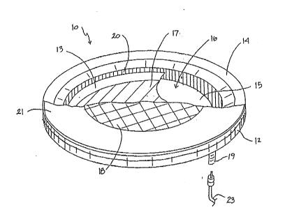
Figure 1 is a perspective view of an embodiment of an
antenna structure of the present invention having
components partially cut away;
F'igure 2 is an exploded view of the embodiment of the
antenna structure illustrated in Figure l;
Figure 3 is a cross-sectional view of a portion of the
antenna structure illustrated in Figure l;
Figures 4 and 5 are exploded and assembled cross-
sectional views~ respectively, of portions of the antenna
structure of Figure 3 taken along axis in 4/5 - 4/5 in
Figure 3;
Figure 6 is an illustration of an application the
present invention in which a rotatable scanned array
antenna is used to communicate with a satellite;
Figure 7 is the layout of the driven elements and the
interconnect network of the scanned array antenna of
Figure 6;
f ~,~;?""~j;
Figure 8 is a cross-sectional view of a portion oE the
scanned array antenna of Figure 6 showing details of a
capacitively coupled, rotatable joint;
Figure 9 is an elevation-plane antenna pattern of the
scanned array antenna illustrated in Figure 6;
Figure 10 is an azimuth-plane antenna pattern of the
scanned array ant~nna illustrated in Figure 6; and
Figure 11 is a plot. of the VSWR of the scanned array
antenna illustrated in Figure 6.
lo Detailed Description of the Invention
The present invention is best understood by referring
to Figures 1-ll of the drawings, like numerals being used
for like and corresponding parts of the various drawings.
Figures 1-5 illustrates an embodiment of an antenna
structure 10 o~ the present invention. It includes a
support member 12 having an upper surface 14 with an
isolating recess 16 disposed thereln and an electrically
conductive reference surface 15 at the bottom of recess 16.
As best shown in Figure 2, support member 12 preferably
comprises an upper support member 34 and a lower support
memb~r 32; and recess 16 is preferably defined by a recess
42 formed in lower support member 32 and an opening 48
formed throu~h upper support member 34. Antenna structure
further includes a radiating means having an
electromagnetically ccupled patch pair (EMCP) of microstrip
elements, namely, a lower, driven, microstrip patch element
17 and an upper, parasitic, microstrip patch element 18.
Parasitic element 18 is disposed so that it is
substantially flush with the region of upper surface 14
surrounding recess 16, but does not contact upper surface
14 or the inner surfaces 20 of recess 16. Driven element
17 is disposed within recess 16 above reference surface 15.
It, too, does not contact the inner surEaces 20 of recess
16. Both parasitic and driven elements 18 and 17 are
substantially parallel to reference surface 15. Parasitic
element 18 can be disposed on a low-loss, insulating sheet
10 21 positioned on upper surface 14. Driven element 17 can
similarly be suspended within recess 16 by disposing it on
another low-loss, insulating sheet 13 positioned within
recess 16 between upper and lower support members 34 and
32. The spaces between parasitic and driven elements 18
15 and 17 and between element 17 and reference surface 15
serve as dielectric layers 31 and 33, respectively, and can
be air or can be filled with a dielectric material,
preferably having a higher dielectric constant than air
(such as a polyurethane foam).
The EMCP pair 17 and 18 transmits or receives radio
frequency ~RF~ signals from or to a radio means, that is a
transmitter and/or receiver, depending upon the
application, by way of a feed means which includes an
interface, such as a coaxial connector 19, to connect
support member 12 with a transmission line or cable 23
coupled to the transmitter/ receiver. As will be discussed
in more detail, an interconnect line 52 connects EMCP pair
17 and 18 to coaxial connector 19.
--10--
f~d ~. ~ 7~ ~i
To provide enhanced i~Dlation for EMCP pair 17 and 18
the surfaces of upper and lower support members 34 and 32,
including inner surface 46 of recess 42 and inner surfaces
and 51 of opening 4~, are preferably electrically
- 5 conductive and are at the same electric potential as
reference surface 15, thereby forming a ground reference
below and around EMCP pair 17 and 18 to substantially
isolate and shield it from nearby electromagnetic fields
and to substantially prevent electromagnetic radiation from
EMCP pair 17 and 1~ from interfering with nearby fields.
To provide such electrically conductive surfaces, upper and
lower support members 34 and 32 can be formed of an
electrically conductive material~ such as aluminum, or can
be formed of a nonconductive material, such as plastic or
structural foam, with the surfaces of upper and lower
support members 34 and 32 and reference surface 15 being
disposed thereon, such as with metallic plating or
conductive paint. Upper and lower support members 34 and
32 can be electrically connected by selecting the size of
lower insulating sheet 13 such that it is smaller than
upper and lower support members 34 and 32, thereby enabling
upper and lower support members 34 and 32 to be in
electrical contact with each other. It can be appreciated
that other means can be used for electrically connecting
the electrically conductive surface.
~ he area of upper surface 14 which surrounds recess 16
is preferably relatively planar to increase the uniformity
of (or reduce distortions to) the radiation pattern of
2 ~ 7 ~
antenna structure 10. The upper edge of opening 48
preferably has a flared ap~rture 51, a feature which has
also been found to enhance the performance of antenna 10
(e.g., beam directivity, reduced coupling). Although
recess 16 and EMCP pair 17 and 18 are illustrated in Figure
1 as being circular in shape, they are not limited to being
any particular shape but may have any number of other
shapes. Driven and parasitic elements 17 and 18 are both
preferably about one-half wavelength elements (facilitating
design and production, particularly when circular
polarization is employed~ but are not limited to such size.
The diameter of the upper end of opening 48 should be
large enough for parasitic element 18 to be positioned
without coming into contact with any of the conductive
surfaces of upper support member 34 or opening 48. If the
distance between the outer edge of parasitic element 18 and
the inner edge of opening 48 is too small, electromagnetic
coupling between the two can occur which changes the
resonant frequency of parasitic element 18 and reduces the
~0 efficiency af antenna structure 10. Increasing the
separation distance reduces such coupling but, as can be
appreciated, an excessive distance between the two can
cause antenna structure lO to take up unnecessary space.
Similarly, the diameter of recess 42 should be large enough
for driven element 17 to fit within recess 42 without
coming into contact with any of the conductive surfaces of
lower support member 32 or recess 42 and should not be so
small that the efficiency o~ antenna structure 10 is
-12-
,5
ad~ersely affected. It has been found that spaciny which
may be desirable between parasitic element 18 and opening
48 is larger than spacing which may be desirable between
driven element 17 and recess 42. The diameter of recess 42
can, therefore, be as large as the diameter of opening 48.
However, it is preferable that recess 42 have a reduced
diameter t~ increase the isolation of microstrip
transmission line 52 by diminishing the amount which is
exposed in recess 42. Flared aperture 51 makes the
lo transition between the two diameters smoother and also
tends to increase the isolation of parasitic element 18.
Use of an EMCP pair increases the bandwidth of antenna
structure 10, with the bandwidth being determined in part
by the thickness and dielectric constant of the material
15 between elements 17 and 18 and between driven elament 17
and reference surface lS. It has been found that the
bandwidth of antenna structure 10 is also determined in
part by the volume of recess 16. Consequently, employing
recess 16 both increases the isolation of EMCP elements 17
and 18 and increases the bandwidth of antenna structure 10.
It has also been found that the performance of antenna
structure 10 is enhanced (e.g., antenna efficiency and
bandwidth) when the distance from an edge of driven element
17 to wall 46 of recess 42 is greater than the distance
between driven element 17 and reference surface 15.
Similarly, it is preferable that the distance from an edge
of parasitic element 18 to the upper edge of flared
aperture 51 be greater than the distance between parasitic
-13-
element 18 and driven ele~ent 17. Without wishing to be
bound by any particular theory, it is believed that such an
arrangement enables one or more radiating apertures to be
defined between parasitic element 18 and dr.iven element 17
and between driven element 17 and reference surface 15
rather than between driven element 17 and adjacent wall 46
and between parasitic element 18 and adjacent flared
aperture 51.
In operation, a signal to be transrnitted by antenna
structure 10 is conveyed to driven element 17 by cable 23
and connector 19. ~It will be appreciated that antenna
structure 10 is equally capable of receiving si~nals and
that the features and advantages of the present invention
are not affected by the mode of operation). ~MCP elements
17 and 18 radiate energy over a bandwidth which is, in
part, determined by the thicknesses and dielectric
constants of dielectric layers 31 and 33 within recess 16.
The present invention employs an EMCP pair and a recess to
increase bandwidth while also providing means to reduce
attendant mutual coupling. Radiated energy yenerated by
elements 17 and 18 within recess 16 which could adversely
affect nearby circuitry or other antenna elements is
substantially confined to the recess by the grounded
surfaces of recess 16. Some of the energy from parasitic
element 1~ radiated away from support member 12 could
similarly adversely affect nearby circuitry or other
antenna elements; the positioning of parasitic element 1~
substantially flush with the surrounding portion of surEace
-14-
14 enables this latter radiation to be substantially
dissipated to conductive surface 14. The substantially
flush nature of parasitic element 18 also facilitates the
low profila and the broad beamwidth of antenna structure
lo. In a like manner, EMCP elements 17 and 18 are
substantially isolated from radiation from external
sourcesO
Thus, the use of EMCP elements 17 and 18 in recess 16
permits antenna structure 10 to exhibit increased bandwidth
over other types of antennas while the use of isolating
recess 16 and conductive surface 14 reduces accompanying
undesirable mutual coupling from that frequently
experienced by conventional EMCP antennas. Further, the
foregoing benefits can be obtained without sacrificing
desirable low profile characteris-tics.
As noted, driven element 17 transmits or receives RF
energy from or to a transmitter or receiver, depending upon
the application. An interface means, such as coaxial
connector 19 secured to the bottom of lower support member
32, is used to connect support member 12 to a transmission
line or cable 23 coupled to the transmitter/receiver. As
illustrated in Figure 3, the outer shielding 132 of co~xial
connector 19 is electrically connected to an electrically
conductive surface of lower support member 32 which is
electrically connected to the other electrically conductive
surfaces of upper and lower support members 34 and 32 such
that all such surfaces are maintained at a common reference
-15-
t .~ ~ Ir t_ ~
voltage (e.g., ground) to provide substantial isolation for
the EMCP pair.
In one aspect of the present invention, the signal-
carrying inner conductor 134 of the coaxial connector 19
extends through lower support member 32 (without contacting
any of the electrically conductive surfaces) and is secured
(such as by soldering) to an interconnect means of a
"square-ax" configuration which interconnects coaxial
connector 19 with driven element 17. A square-ax
transmission line includes an insulated, inner, signal-
carrying conductor surrounded by an isolating "channel"
shield through the support member which is connected to a
reference voltage (e.g~ ground).
The signal-carrying conductor of che square-ax
transmission line employed in the present invention
includes a microstrip transmission line 52 and a two-way
polarizer comprising microstrip lines 58 and 59 of unequal
lengths to obtain circular polarization, as desired. It
will be appreciated that other techniques can he used to
obtain circular polarization. Lines 52, 58 and 59 are
disposed on the same surface of lower dielectric sheet 13
as driven element 17 and are coplanar therewith and
connected thereto. The shielding portion of the square-ax
transmission line includes lowe~ channel portions 54, 55
and 57 disposed in the top of lower support member 32 and
upper channel portions 56, 61 and 63 (shown in phantom)
disposed in the bottom of upper support member 34. The use
of two support members facilitates production by enabling
-16-
~'~, 7.~ L~2~j
upper and lower channel portions to be formed separately
and permits a more complicated interconnect arrangement
than would otherwise be possible.
The inner surfaces of channel portions 54, 55, 56, 57,
61 and 63 are electrically conductive to provide the
desired shielding around lines 52, 58 and 59. Both lower
channel portions 54, 55 and 57 and upper channel portions
56, 61 and 63 correspond generally in position and geometry
to lines 52, 58 and 59 but are slightly wider to prevent
lines 52, 58 and 59 from contacting any of the electrically
conductive surfaces or channels. When lower insulating
sheet 13 i5 secured between upper and lower support members
34 and 3z, lower and upper channel portions 54, ~5 and 57
and 56, 61 and 63, respectively, form a continuous channel
in which lines 52, 58 and 59 are suspended. Thus,
electromagnetic fields created around signal-carrying lines
52, 58 and 59 are substantially confined to the channels in
which t~e lines are suspended. Additionally, lines 52, 58
and 59 are shielded ~rom nearby fields.
As previously noted, a two~way polarizer comprising
microstrip lines 58 and 59 can be employed to excite driven
element 17 in two orthogonal modes, thus achieving
circularly polarization. It can be appreciated that both
le~t- and right-hand circular polarization can be
accommodated. Additionally, linear polarization can be
achieved by exciting driven element 17 directly ~rom
microstrip transmission line 52 without a two-way
polarizer. The driven element can also be rectangular and
two orthogonal modes can be excited by using a two-way
polarizer coupled to adjacent sides o~ the patch or by
exciting the patch at a corner; linear polarization can be
provided by exciting the rectangular patch on one side.
Driven elemant 17 and lines 52, 58 and 59 can be
disposed on lower insulating she~t 13 usiny conventional
thin-film photo-etching techniques. For example, the top
or bottom surface of lower insulating sheet 13 can be
completely metallized using conventional thin-film
deposition techniques and then unwanted metallization can
be etched away leaving driven element 17 and lines 52, 58
and 59. Parasitic element 18 can also be disposed on the
upper or lower surface of upper insulating sheet 21 using
thin-film techniques. Alternatively, conventional thick-
film silk-screening techniques can be used to provide the
metallizations.
As an alternative to employing square-ax transmission
lines, the inner signal-carrying conductor 134 of coaxial
connector 19 secured to the bottom of lower support member
32 can extend through lower support member 32 (without
contacting any electrically conductive surfaces) into
recess 42 and be connected (such as by soldering) directly
to driven element 17. If inner conductor 134 is connectsd
to the center of driven element 17, a monopole radiation
pattern results. It can be appreciated that other patterns
will result when the connection is made at other locations
on driven element 17. Outer shielding 132 of coaxial
connector 19 is electrically connected to an electrically
-18-
conductive surface of lower support member 32 to provide
the reference voltage.
Figure 3 is a cross-sectional view of a portion of
antenna structure 10 of Figure 1 to further illustrate the
arrangement of the individual elements. In particular,
parasitic element 18 is substantially flush with the reyion
of upper surface 14 surrounding opening 48. Consequently,
extraneous fields and radiation from parasitic element 18
are either substantially confined to opening 48 or are
dissipated to ground by upper surface 14.
Figs. 4 and 5 are exploded and assembled cross-
sectional views, respectively, of a portion of antenna
structure 10 taken along axis 4/5 - 4/5 of Figure 3. They
illustrate the manner in which microstrip transmission line
58 is suspended within an isolating channel comprising
lower channel portion 57 and upper channel portion 61.
Consequently, electromagnetic fields created around
transmission line 58 are substantially confined to the
channel defined by upper and lower channel portions 61 and
57 in which transmission line 58 is suspended.
In the embodiment illustrated, upper and lower channel
portions 61 and 57 are each rectangular in cross-section;
each may, however, have other cross-sectional geometries
such as, for example, semi-circular. The channel must be
large enough to prevent the microstrip transmission line
from contacting any electrically conductive surface but
should not be so large that it uses an excessive amount of
space. It has also been found that enlarging the size of
the channel results in a_ lower current density in the
conductive walls contributing to lower losses and greater
efficiency in antenna structure 10.
The b~nefits of the present invention are particularly
realized in an array in which isolation of the radiating
elements and interconnect network, the ability to track
another station, and a low profile are especially
important. Figure 6 illustrates such an application in
which a satellite 62 is in a geQstationary orbit and
positioned at an angle a relative to a specific region of
the earth. A fixed ground station employing an antenna
structure can often be aimed broadside at satellite 62 and
fixed in that position to obtain satisfactory communication
with satellite 62. However, in a mohile applicakion,
particularly one in which a low profile or concealable
antenna is desired, continuous broadside tracking may be
difficult as the vehicle changes locations. For such an
application, the present invention can be configured into
a scanned array antenna system, indicated as 64 in
Figure 6. A particular scan angle ~, providing a desired
scan volume, can be obtained by appropriate selection of
the number of antenna elements 66 in isolating recesses in
the array, their arrangement on a support member 68, the
spacing between them and their phasing relative to each
other.
In the embodiment illustrated in Figure 6 and detailed
in Figure 7, ten driven elements 70, 71, 72, 73, 74, 75,
76, 77, 78 and 79 are arranged to be symmetrical across an
-20-
2 ~ 7 ~ n ~ ~ 5
axis Z-Z which is perpendicular to the scanning direction,
indicated by an arrow 69. As the vehicle on which antenna
array 64 is mounted moves and changes its ~irection,
support member 68 can be rotated about a center axis by a
motor 65 under the control of a control module 67 in order
to keep geostationary satellite 62 within the scan volume.
Other conventional devices can be used to drive support
member 68. As will be explained in detail in conjunction
with Figure 8, a transition means can be employed to couple
an interconnect means, connected to antenna elements 66,
with an interface means, including a coaxial connector to
permit relative rotation between the interconnect means and
the interface means. Alternatively, antenna array 64 can
be electrically scanned when appropriate circuitry is
employed.
Figure 7 illustrates particular aspects of scanned
array antenna 64 in more detail. Driven elements 70-79 are
disposed on an insulating sheet 80, such as a thin Mylar
sheet. The interconnect means includes an interconnect
Z~ network ~2 of microstrip transmission lines, also disposed
on insulating sheet 80. The transition means includes a
feed patch 84 positioned approximately in the center of
insulating sheet 80 which couples driven elements 70-79 to
the transmission means. Insulating sheet 80 is positioned
on a lower support member and covered with an upper support
member, the two support members together comprising support
member 680 Parasitic elements, which substantially
correspond in shape and position to driven elements 70-79,
ftd ~ '.,&.~
are disposed on a second insulating sheet positioned above
the upper support member. Channels are disposed in support
member 68 which substantially correspond to the
configuration of interconnect network 82 and result in a
square-ax network in which the signal-carrying microstrip
transmission lines of interconnect network 82 are enclosed
within and isolated by the channels in support member 68.
Feed patch 84 is preferably soldered to the center
conductor of a coaxial connector secured to the bottom of
support member 68. The center conductor is disposed
through the lower support member without contacting any of
the electrically conductive surfaces of support member 68.
These cond~ctive surfaces are connected to ~he outer
shielding of the coaxial connector thereby providing
shielding for interconnect network 82.
To provide the ~canning direction and angle
illustrated in Figure 6, interconnect network 82 includes:
a first feed patch segmen~ 86 connecting driven elements
70, 71 and 72 with feed patch 84; a second feed seyment 88
connecting driven elements 73 and 74 with feed patch 84; a
third feed seyment 90 connecting driven elements 75 and 76
with feed patch 84; and, a fourth feed segment 9~
connecting driven elements 77, 78 and 79 with feed
patch 84.-
Driven elements 70-79 are dual-fed in phase quadrature
to excite orthogonal modes and obtain the circular
polarization desired for ground-to-satellite
communications. Additionally, the lengths of the
-22-
microstrip transmission lines in each of first, second,
third and fourth feed segments 86, 88, 90 and 92 differ in
length to provide phase shifting of the signal supplied to
the four groups of driven elements 70-~2, 73 and 74, 75 and
76, and 77-7g relative to each other. Directional scanning
results in the direction indicated by arrow 69.
One method for increasing scan angle e is to decrease
the spacing dl between adjacent radiating members in the
scanning direction. A beneficial consequence of the
reduced spacing is a reduction in grating lobes which t~nd
to reduce the antenna's efficiency. HoweYer, decreasing
spacing dl increases the likelihood of undesirable coupling
among adjacent radiating members and microstrip
transmission lines. Decreasing the spacing may also make
it more difficult to lay out intersonnect network 82
between elements 70-79. Both of these problems can be
partially alleviated by increasing the spacing d2 in the
non-scanning direction between adjacent radiating members
in the same row. Spacing d2 should not be increased so
much, however, that excessive grating lobes adversely
affect antenna performance. Spacing d3 in the non-scanning
direction between radiating members in adjacent rows is
pre~erably about one-half d2, providing a substantially
uniform radiation pattern with satisfactory gain and
reduced coupling in a given amount of space.
As previously detailed, the present invention reduces
adverse mutual coupling while increasing bandwidth and
substantially maintaining spacing to obtain a desired scan
-23-
angle by disposing each radiating member in array antenna
64 in an isolating recess and by disposing interconnect
network 82 in isolating square-ax channels. The
electromagnetic fields created around transmission lines in
interconnect network 82 are substantially confined to the
isolating channels in which the lines are suspended. The
electromagnetic fields created around and below each of
driven patches 70-79 are substantially confined to the
isolating recess in which each is located. And, extraneous
fields and radiation from the parasitic patches are either
substantially confined to the openings in support member 68
in whi~h the patches are located or are substantially
dissipated to ground by the electrically conductive upper
surface of support member 68. Such an arrangement of
lS recesses and channels also substantially shields the
transmission lines of interconnect network 82 and the patch
elements from nearby electromagnetic ~ields.
Furthermore, as with the embodiment of the present
in~ention descri~ed in conjunction with Figures 2-5, the
recesses in support member 68 o~ array antenna 64 can have
flared apertures to reduce mutual coupling and to increase
the isolation of portions of inter~onnect network 820
It will be appreciated that other arrangements of
antenna elements 66 are possible and that greater or fewer
numbers of them can be used. For example, the gain of
array antenna can be increased if a greater number of
antenna elements 66 are used. If high gain is not
required, a scan angle capability and bandwidth adequate
-24-
~,~ s7 ~ ~ ,5
for certain applications can be provided using as few as
three antenna elements 66, thereby reducing the overall
size of array antenna 64.
When antenna elements 66 are circular in shape, as
illustrated in Figures 6 and 7, the layout of interconnect
network 82 is facilitated. However, other shapes, such as
rectangular, can also be used.
Because certain applications of the present invention
require that it be exposed to the elements, a protective
radome may be desired. To simplify construction and
enhance performance, the upper parasitic patch(es) can be
disposed on the inside surface Qf a close-fitting radome
and still be located in a substantially flush position over
the opening(s) in the support member.
Figure 8 illustrates a cross sectional view of the
center portion of scanned array antenna 64 of Figure 6
along axis Z-Z, including the transition means. The
transition means includes means for capacitively coupling
the signal-carrying conductor of the interconnect means
with the signal-carrying conductor of the interface means
and also for capacitively coupling khe reference (i.e.,
ground) conductor of the interconnect means with the
reference conductor of the interface means. Referring to
Figure 8 for more detail, support member 68 includes an
upper support member 94 and a lower support member 96, both
of which can be formed of an electrically conductive
material, such as aluminum, or from a nonconductive
material, such as plastic or structural foam, and coated
-25-
;~ 7.~
with an electrically conduc~ive material~ Lower insulating
sheet 80 is disposed between upper and lower support
members 94 and 96. Feed patch 84, first feed segment 86
and fourth feed segment 92 are disposed on one surface of
lower insulating sheet 80. . The balance of interconnect
network 82, shown in detail in Figure 7, is also disposed
on lower insulating sheet 80. An upper insulating sheet 98
is positioned above upper support member 94 and has
parasitic elements disposed thereon. ~pper channels 100
and 101 are formed in the lower surface of upper support
member 94 and lower channels 102 and 103 are formed in the
upper surface in lower support member 96. Together they
form the channels in which first and fourth feed segments
86 and 92 are suspended. Upper channels 100 and 101 open
into an upper cavity 10~, ~ormed in the lower surface of
upper support member 94, which is substantially aligned
over feed patch 84. Lower channels 102 and 103 open into
a lower cavity 105, formed in the upper surface of lower
support member 96, which is substantially aligned under
feed patch 84.
Included in the interface means is a conventional
coaxial connector 106 which fits in a recess 108 formed in
the lower surface of lower support member 96. Coaxial
connector 106 has an electrically conductive outer shell
110 which is connected to a reference potential, or ground,
and surrounds a signal-carrying inner conductor 112. Whsn
assembled, inner signal-carrying conductor 112 is
electrically secured, such as by soldering, to a coupling
-26-
disk 114 of th~ transition means located betw~en upper
support member 94 and lower insulating sheet 80.
Also included in the transition means are: a first low
friction layer 116 disposed between coupling disk 114 and
feed patch 84; a second low ~riction layer 118 disposed in
cavity 10~ between lower support member 96 and outer shell
llO of coaxial connector 106; and a third low friction
layer lZ0 disposed between coaxial connector 1~6 and a
closure plate 122. When secured to lower support member 96
with screws 124 or other fasteners, closure plate 122
contains second low friction layer 118, coaxial connector
106 and third low ~riction layer 120 within recess 108.
Third low friction layer l~0 and closure plate 122
each have a hole formed through their centers and fit onto
the lower end of coaxial connector 106. Similarly, second
low ~riction layer 118 has a hole formed through its center
and fits onto the upper end of coaxial connector 106 before
coaxial connector 106 is inserted into recess 108. Holes
in lower insulating sheet 80, feed patch 84, first low
friction layer 116 and coupling disk 114 permit them to fit
onto signal-carrying conductor 112 before it is secured to
coupling disk 114.
Each of first, second and third low friction layers
116, 118 and 120 are preferably disk shaped pieces of thin
material having a low coefficient of friction, such as
Teflon. Thus, two components separated by a low friction
layer can rotate smoothly relative to each other.
Additionally, each low friction layer preferably comprises
-27-
a dielectric material to serve as an insulator between
adjacent conducting surfaces.
In operation, a coaxial cable from a transmitter,
receiver or transceiver is fastened to the interface means
(e.g., coaxial connector 106). The connector and cable
remain in a position which is fixed relative to the
transmitter/receiver which is attached to, for example, a
moving vehicle. When the vehicle changes its orientation
relative to a particular satellite, it is desired that
scanned array antenna 64 remain locked onto the satellite.
Control module 67 activates tracking motor 65 which causes
upper and lower support members 94 and 96, upper and lower
insulating sheets 98 and 80, along with feed patch 84 and
interconnect network 82, and enclosure plate 122 to rotate
by an amount substantially equal to the rotation of the
vehicle, but in the opposite direction. Coupliny disk 114,
which is secured to signal-carrying conductor 112 of
coaxial connector 106, remains fixed relative to the
vehicle. First, second and third low friction layers 116,
20 118 and 120 permit the components of array antenna 64 to
move smoothly relative to each other.
In the transition means, coupling disk 114 and feed
patch 84, separated by a low friction layer serving as a
dielectric, are capacitively coupled as indicated by ~irst
field 126. Thus, a signal being carried by signal-carrying
conductor 112 can be passed to feed patch 84 and the
balance of int~rconnect network 82. The relative motion
-28-
..b-,w~
between coupling disk 11~ and feed patch 84 does not
substantially affect first field 126.
Similarly, the rsference potential ~or ground) of
outer shell 110 i5 capacitively coupled to lower support
5 member 96 by a second field 128. Outer shell 110 and lower
support member 96 are separated by a low friction layer,
serving as a dielectric. F'urthermQre, closure plate 122 is
preferably electrically conductive causing a third field
130 to be established between outer shell 110 and closure
plate 122, also separated by a low friction layer serving
as a dielectric. Because capacitance is proportional to
the total area of the capacitive plates, the use of
capacitive plates, such as lower support member 96 and
closure plate 122, on both sides of outer shPll 110
increases the ground coupling (capacitance) without
increasing the area of the capacitive plates or permits th~
area o~ the capacitive plates to be reduced while still
maintaining satis~actory ground coupling.
Consequently, an antenna such as scanned array antenna
64, can he electromagnetically coupled to both the signal-
carrying conductor and the ground conductor of a fixed feed
line, such as a coaxial cable, and be rotated without
relying on complicated mechanical joinks which employ
direct physical and electrical contact between rotating
parts. Such mechanical joints are subject to wear due to
~riction and can introduce electrical noise when oxidation
or contaminants build up between rotating parts. Thus,
per~ormance tends to degrade. However, such shortcomings
-29-
2~ 6.~S
are substantially reduced in the transition of the present
invention which does not rely on direct physical and
electrical contact between rotating parts.
It will be appreciated that the alectromagnetically
coupled transition described herein is not limited to a
rotary joint or to a connection between a coaxial cable and
an antenna. It can be used to connect lines of various
types such as coaxial to coaxial, microstrip to microstrip,
and combinations of these and other lines. It can also be
employed when it is necessary to make a 90 degree
transition or when it ~s difficult or undesirable to attach
a feed connector to one side of a board. The latter
situation might exist, ~or example, when a transition must
be made to a microstrip transmission line (comprising a
microstrip line disposed above a ground line or plane)
which is ~ealed inside a module. A coupling disk, attached
to a signal-carrying conductor, can be secured to the
surface of the module closest to the internal microstrip
line and a grounding disk, attached to a ground conductor,
can be secured to the surface of the module closest to the
internal ground line or plane. Thus, coupling can be made
to the sealed module without penetrating the module.
Example
An exemplary scanned array antenna, such as array
antenna 64 illustrated in Figures 6 and 7, has been
constructed for right-hand circular polarization in the L-
band with ten EMCP pairs and aluminum support members. The
-30-
driven and parasitic elements were approximately one-half
wavelength copper elements, the driven element being
disposed on thin mylar film and the parasitic element being
disposed on a thicker polycarbonite sheet which also served
as a protective radome.
Figures 9, 10 and 11 graphically illustrate the
results of tests of the exemp}ary scanned array antenna.
Figure ~ illustrates an elevation-plane antenna pattern
with a source transmitter having a frequency of 1560 MHz
located at an azimuthal posi-tion ~=0.
Figure 10 graphically illustrates an azimuth-plane
antenna pattern with a source transmitter having a
frequency of 1560 MHz located at an elevation e=300.
Figure 11 illustrates the voltage standing wave ratio
(VSWR) oE scanned array antenna 64 with the frequency
varying from 1500 to 1700 MHz.
These and other tests provide the following
performance characteristics:
VSWR: less than about 1.6:1
Bandwidth: greater than about 10%
Gain: about 14.2 dB (typical)
Axial ratio: about 2 dB
Beam widths: azimuth: about 20
elevation: about 38
Peak side lobe level: azimuth: about -13 dB
elevation: about -10 dB
-31-
~ r
As will be appreciate~ by those skilled in the art,
the ~oregoing antenna array represents a significant
advance where broad bandwidth, low mutual coupling and wide
scan angle needs exist. Further, these needs can be met
S without sacrificing low profile capabilities.
Although the present invention has been described in
detail, it should be understood that various changes,
substitutions and alterations can be made herein without
departing from the spirit and scope of the invention as
defined by the amended claims.