Note: Descriptions are shown in the official language in which they were submitted.
i
207I~89
LUMINOUS PANEL DISPLAY DEVICE
BACKGROUND OF THE DISCLOSURE
The invention is in the field of luminous
displays and signs, and more particularly relates to
gas plasma display devices.
The production of light by the passage of
electricity through gases is a well known
phenomenon. Devices utilizing this phenomenon have
been widely developed in the form of plasma display
devices which display specific numerals, characters,
symbols, graphics, and the like. The neon sign is an
example of a gas discharge display device, typically
including an elongated glass tube filled with neon
and a pair of excitation electrodes disposed at
opposite ends of the tube. In this example, the
rigid tube, or envelope, defines the shape of the
illumination pattern. This shape is established at
the time of manufacture, and cannot be changed.
Other prior art gas discharge display
devices may include a plurality of shaped character
electrodes in direct or close contact with an
electroluminescent gas Within a glass envelope, for
example, Nixie tubes. In such devices, selected ones
of the shaped electrodes may be energized to obtain a
desired character display. Again, the shape of the
illumination is predetermined by the shape of the
electrode which is established at the time of
manufacture of the device.
20~i489
-2-
Still other forms of prior art gas discharge
display devices include dielectric-bounded,
gas-filled character-shaped channels within an
envelope, with a suitable set of energizing
electrodes. As in U.S. Patent No. 3,621,332, a
plurality of such channels may be established within
a single envelope, with electrodes being arranged for
selective activation of one channel at a time.
Alternatively, as in U.S. Patent No. 4,584,501, a
single elongated channel may be formed in one plate
of a two glass plate sandwich arrangement, with
energizing channels in an adjacent plate. All of
these arrangements are suitable for displaying
indicia, but as with the earlier discussed prior art,
the shape of the display, i.e. the channel
configuration, is determined at the time of
manufacture of the device.
Yet other prior art gas discharge devices
include generally similar display configurations, but
have an addressable matrix in which selected dot
regions may be selectively energized. For example,
as shown in U.S. Patent No. 4,035,690, selected ones
of overlapping orthongal sets of electrodes may be
energized to generate a desired dot matrix
character. In that patent, the electroluminescent
gas is confined to the interior of a plurality of
dielectric spheres disposed between the sets of
electrodes. kith the dot addressible matrix,
substantial flexibility is provided in that any dot
pattern graphics may be displayed, for example using
conventional bit-mapped graphics techniques.
However, as with the other above mentioned prior art,
2fl714~9
-3-
all possible display patterns, i.e. the electrode
overlap regions, are established at the time of
manufacture of the device.
Yet another form of prior art gas discharge
device is disclosed in U.S. Patent No. 3,629,654. As
shown in that patent, a pair of opposed, spaced apart
plates are mutually sealed at their perimeter. to
establish an electroluminescent gas filled cell. A
transparent conductive coating is disposed on one
outer surface of the cell. A movable external sheet
having predetermined shaped conductive regions is
pressed against the other outer surface of the cell
and an ionizing signal is applied across the
conductive coating and the conductive region of the
external sheet to generate a visible discharge in the
cell having the shape of the conductive regions of
the external sheet. This two-element display thus
requires a means for positioning the external sheet
relative to the cell in order to establish an image.
It is an object of the present invention to
provide an improved plasma display device.
Another object is to provide an improved
plasma display device which may be user-programmed
for the display of a desired image.
Yet another object is to provide an improved
plasma display which may be economically and
efficiently configured to display a desired image.
2071489
-4-
SUMMARY OF THE INVENTION
Briefly, the present invention is an
electroluminescent gas filled double walled panel
with the provision for electrode surfaces on both
sides of the gas space, which will allow for a
luminous gas (or plasma) discharge to be generated
when suitably energized. The electrode surfaces may
be indicia-(or other graphic image-)shaped, thus
producing a like shaped pattern of light of
sufficient visibility to be useful as a sign,
indicator or other expression of visible information.
The pattern of at least one of the electrode
surfaces may be provided by a secondary manufacturer,
for example, a user, through the means of painting,
stencilling, silkscreening, lithography or the like.
By so providing the latter electrode surfaces, the
inherent difficulties and costs of producing signage
(for example, using a heat-bent gas discharge tube of
conventional neon tube signs) are overcome, while
still producing a luminous gas image. Thus, even a
small signage producing enterprise, or home user, may
readily utilize the display device of the present
invention to display a user desired image.
Additionally, the display panel of the
present invention is far more robust, durable and
safe than its bent tube neon sign counterpart. In
some configurations, the display device has
transparent electrodes on both sides of the gas
space, making the display device usable as a window
or glass door simultaneously with its carrying images
or information.
2o7~~s~
-5-
The display panel may also find general
usage in the architectural and outdoor illumination
field, much as its bent tube neon sign counterpart
does currently. Similarly, much as artists and
designers use light filled tubes as components of
graphic and sculptural statements, the light
producing display devices of the invention may be
used, with or without patterns to the illuminosity,
as an artistic and design medium.
More particularly, in accordance with the
invention, a display device includes first and second
non-conductive sheet members, each having front and
back surfaces, which may be substantially parallel.
At least one of the first and second sheet members is
transparent.
In a preferred form, the sheet members are
rigid and substantially planar, but alternative
configurations could be employed, such as similar
cylindrical or spherical configurations, or non-rigid
configurations. By way of example, the sheet members
may be planar sheets of glass. The first sheet
member may be substantially transparent and has a
coating region on its front surface adapted to
receive a first conductive coating (a "pattern
electrode") on portions thereof. Typically, this
first conductive coating represents the image to be
displayed. The first conductive coating may be
removable in part to correspond to a modified form of
the image. The second sheet member may also be
transparent. The first conductive coating may be
applied by painting, stencilling, silkscreening,
lithography, or the like.
207i4~~
-6-
One or more spacer elements mutually
position the first and second sheet members so that
the back surface of the first sheet member is offset
from and opposite the front surface of the second
sheet member.
A discharge chamber is established by a gas
impervious seal between portions of the back surface
of the first sheet member and the front surface of
the second sheet member. The discharge chamber
defines a closed region in the gap between the back
surface of the first sheet member and the front
surface of the second sheet member. That closed
region underlies at least in part the first
conductive coating.
An electroluminescent gas is disposed within
the closed region. While other gas mixtures may be
used, in the preferred form the electroluminescent
gas is a Penning gas mixture comprised substantially
of 99% neon, 1% argon, and trace amounts (less than
0.1%) of mercury at a pressure of about 120 torr.
In one form of the invention, a second
conductive coating (i.e. a conductive element or
"charging electrode") is disposed on a portion of one
of the front and back surfaces of the second sheet
member underlying at least in part the closed region
and a part of the coating region. In other forms,
the charging electrode may not underlie the first
conductive coating, while still being on one of the
front and back surfaces of, or within, or adjacent to
the second sheet member. By way of example, the
charging electrode may be a wire (e.g. extending at
207149
least partially through the closed region, or
embedded in the second sheet member), or it may have
the form of a conductive portion of the seal which
establishes the chamber.
An applied drive voltage may be coupled
between the first conductive coating and the charging
electrode to energize the device so that a luminous
plasma image is established in the portions of the
closed region adjacent to the first conductive
coating.
In one form of the invention, the spacer
includes at least one rigid spacer member disposed
within the closed region and extending between the
back surface of the first sheet member and the front
surface of the second sheet member.
In various embodiments, either or both of
the first and second conductive coatings may be
substantially translucent, transparent, reflective or
opaque. Further, the conductive coating forming the
charging electrode may be disposed on the front
surface of the second sheet member and at least in
part within the closed region. Alternatively, the
second conductive coating may be disposed on the back
surface of the second sheet member and at least in
part overlying the closed region. A third
non-conductive sheet member may overlie the second
conductive coating opposite the back surface of the
second sheet member. A fourth non-conductive sheet
member may overlie the first conductive coating. The
latter non-conductive sheets may be used to ensure
that a user does not contact the electrodes during
CA 02071489 2001-06-11
_g-
use. Further, those added sheets provide increased
resistance to breakage of the device as a whole. Also,
those sheets, when laminated to the first and second
sheets, provide ir:creased stiffness of the chamber-
s defining walls so that. relatively thin sheets may be used
for the first and second sheet members, using relatively
inexpensive (e.g. polycarbonate) material to form the
third and/or fourth sheet members.
Various forms of the invention may be adapted
to minimize radio frequency interference (RFI) by using
shielded configurations, for example where a grounded,
conductive element: is disposed over the charging
electrode. Dual back-t:o-back displays may be used where
an opaque element is disposed between the illuminated
regions, so =hat :independent images may be established in
those regions for viewing from opposite sides of the
display devi:~e .
Accordingly, in one aspect, this invention
provides a luminoi.ls panel display device comprising:
A. a first: non-conductive sheet member having
front anal bae:k su~:~faces, said first sheet member having a
coating region on portions of its front surface, said
coating region being adapted to receive a first
conductive coatincr representative of a predetermined
image;
B. a ::>econd non-conductive sheet member
having front and back surfaces, wherein at least one of
said first and second sheet members is transparent;
C. spacer means for mutually positioning said
first and second sheet: members whereby the back surface
CA 02071489 2001-06-11
-8a-
of said first sheet :member is offset by a predetermined
separation f.r_om and opposite the front surface of said
second sheet member;
D. di~~charge chamber means for establishing a
gas impervious seal between portions of the back surface
of said first sheet member and the front surface of said
second sheet member to define <~ closed region in the gap
between said back surface of said first sheet member and
the front surface of said second sheet member and
underlying said coating region;
E. electroluminescent gas disposed within
said closed region; anal
F. a conductive el.=ment disposed on a portion
of one of the front and back surfaces of, or within, or
adjacent to, said second sheet member, wherein said
conductive element: is a wire positioned on the surface of
or within said second sheet member.
In a further aspect, this invention provides a
luminous pana_1 d,~splay device comprising:
A. a first non-conductive sheet member having
front and ba<:k surfaces, said first sheet member having a
coating regi~:m on portions of its front surface, said
coating region be.i.ng adapted to receive a first
conductive coating representative of a predetermined
Image;
B. a ~secord non-conductive sheet member
having front and back surfaces, wherein at least one of
said first and second sheet members is transparent;
C. spacer means for mutually positioning said
first and second sheet. members whereby the back surface
of said firsO, sheet member is offset by a predetermined
CA 02071489 2001-06-11
-8b--
separation from and o~>posite t'ne front surface of said
second sheet membE:r;
D. discharge chamber means for establishing a
gas impervious seal between portions of the back surface
of said first sheet. member and the front surface of said
second sheet member to define a closed region in the gap
between said back surface of said first sheet member and
the front surface of said second sheet member and
underlying said coating region;
E. electroluminesc~~nt gas disposed within
said closed region; and
F. a conductive element disposed on a portion
of one of the front and back surfaces of, or within, or
adjacent to, said second sheet member, wherein said
conductive e.:Lement is a wire extending at least partially
through said closeed region.
In a st~.ll further aspect, this invention
provides a luminous panel display device comprising:
A. a First non-conductive sheet member having
front and back surfaces, said first sheet member having a
coating region on portions of its front surface, said
coating region being adapted to receive a first
conductive coating representative of a predetermined
image;
B. a second non-conductive sheet member
having front and back surfaces, wherein at least one of
said first and sec:vo~~d sheet members is transparent;
C. spacer means for mutually positioning said
first and second v;heet. members ~ahereby the back surface
of said first sheet member is offset by a predetermined
CA 02071489 2001-06-11
-gc__
separation from and o~>posite the front surface of said
second sheet member;
D. discharge chamber means for establishing a
gas impervious seal between portions of the back surface
of said first sheet member and the front surface of said
second sheet member to define a closed region in the gap
between said back surface of said first sheet member and
the front surface of said second sheet member and
underlying said coating region;
E. electroluminescent gas disposed within
said closed region; and
F. a ~::onduc~ive element disposed on a portion.
of one of th~~ front and back surfaces of, or within, or
adjacent. to, said second sheet member, wherein said
conductive elemen-,~ extends at least partially around the
periphery of said closed region, and wherein said
conductive elemen.-.. is integral with said spacer means.
In a further aspect, the present invention
provide. a lumino~.zs panel display device comprising:
A. a (first non-conductive sheet member having
front and back sur_~fa~~es, said first sheet member having a
coating region on portions of its front surface, said
coating region, being adapted tc receive a first
conductive coatincx representative of a predetermined
image;
B. a .=.second nor.-conductive sheet member
having front and back surfaces, wherein at least one o-_.
said first and se~:ond sheet members is transparent;
C. spacer means for mu'ually positioning said
first arid se~~ond sheet. members whereby the back surface
of said first sheet member is offset by a predetermined
CA 02071489 2001-06-11
_gd__
separation from and opposite the front surface of said
second sheet member;
D. discharge chamber means for establishing a
gas impervious seal between portions of the back surface
of said first sheet member, and the front surface of said
second sheet member to define a closed region in the gap
between said back surface of said first sheet member and
the front surface of ;aid second sheet member and
underlying said coating region;
E. electroluminescent gas disposed within
said closed region; and characterized in that: a
conductive e:Lement~ is disposed embedded within said
second sheet member in the form of a wire, wire grid or
woven wire mesh o~- is disposed adjacent to said second
sheet member but not underlying said coating region.
BRIEF DESCRI°TION OF THE DRAWINGS
T'~e forE.=aoir:g and other objects of this
invention, the vaz:ious features thereof, as well as the
invention itself, may be more fully understood from the
following de:;cript.ion, when read together with the
accompanying drawings in which:
Fi~:~. 1 shows in exploded form, a display device
according to the present invention;
Fig. 1A shows, in section, the portion of the
display devi,re of FIG. 1 i:.cluding the filling stem;
Fi~:~. 1B shows in exploded form, another
embodiment of the present invention;
20~14~9
-9-
Fig. 2 shows in exploded form, an
alternative display device configuration;
Figs. 2A-2D show in perspective view
variations of the display device shown in Fig. 1;
Fig. 3 shows in perspecitve view, a plasma
display device having a plurality of internal spacers;
Fig. 4 shows in section along lines 4-4, the
plasma display device of Fig. 3;
Fig. 5 shows a perspective view of an
alternative spacer for use with the device of Figs. 3
and 4;
Figs. 6-9 show sectional views of
alternative spacers for use with the device of Figs.
3 and 4;
Fig. 10 shows in exploded form, an
alternative configuration for a plasma display device
of the present invention; and
Figs. 11 and 12 show perspective views of
one edge of dual display devices embodying the
invention.
2~714~9
-10-
DESCRIPTION OF THE PREFERRED EMBODIMENT
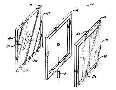
An exemplary luminous (plasma) panel display
device 10 is shown in Fig. 1 in exploded form. The
device 10 includes two flat and parallel
non-conducting, transparent glass sheet members 12
and 14 having "front" surfaces 12a and 14a,
respectively, and "rear" surfaces 14a and 14b,
respectively. As shown, sheet members 12 and I4 axe
substantially planar, but other forms might also be
used, such as cylindrical or conical.
An edge seal and spacer element 16 defines
an enclosed hermetic volume (or region) 20 having an
electroluminescent gas therein. Overlapping
conductive coatings 26 and 28 are disposed on the
front surface 12a of sheet member 12 and on the rear
surface of 14b of sheet member 14, respectively. In
alternative embodiments, a conductive element that
generally corresponds to coating 28 may be used,
where that element may not overlap any portion of a
conductive coating corresponding to coating 26 (for
example, as described below in conjunctian with Figs.
2A-2D), and where that element may not be a coating
(for example, as described below in conjunction with
Figs. 2B-2D).
In the embodiment of Fig. 1, a filling stem
22, extending parallel to the principal plane of
volume 20, passes between opposing portions of sheet
members 12 and 14 and through spacer member 16 to
provide access to chamber volume 20. The outer
diameter of filling stem 22 is less than or equal to
the distance between the front surface 12a and the
a
2~'~I48~
-11-
back surface 14b: This filling stem 22 permits
evacuation and back-filling of the volume 20
following assembly of sheet members 12, 14 and
seal/spacer element 16. After back-filling is
accomplished, the stem 22 is sealed off. In
alternative embodiments, different filling stem
configurations may be used. For example, the stem
may be placed through a hole drilled through sheet
member 12 and fused to the edges of that hole, with
the central axis of the stem extending perpendicular
to the principal plane of volume 20.
In the preferred embodiment, the sheet
members 12 and 14 axe non-conductive soda-lime planar
glass sheets. The spacer element 16 is also
soda-lime glass. The thickness of the sheets is
determined to establish (1) a parallel orientation of
the two sheets, producing a gas-enclosing space with
uniform gap after filling, and (2) total mechanical
and thermal stress on the glass sheet members during
the assembly and evacuation of the device 10 which
does not exceed the properties of the glass, causing
breakage. The preferred embodiment has an enclosed
volume which is 15 cm by 15 cm, with an intersheet
gap in the range 0.25 - 1.0 mm, as established by
spacer 16. The soda-lime glass sheet members 12 and
14 are 3.0 mm thick. With larger surface areas,
thicker glass sheets may be used, and for smaller
areas, thinner glass may be used. For glass with
higher resistance to temperature stressing and higher
mechanical strengtr:, such as borosilicate glass, the
20~~48~
-12-
thickness required for any specific surface area may
also be reduced im comparison to the soda-lime glass
sheets used in the illustrated embodiment. For
example, a 15 cm by 15 cm chamber formed by Pyrex
brand borosilicate glass sheets with a 1 mm gap, may
have 2.5 mm sheet thickness without overstressing.
The embodiment of Fig. 1 is a three element
construction (i.e. sheet members 12, 14 and spacer
element 16). Other configurations might also be
used, for example, two sheet members in a sandwich
configuration where one or both of the adjacent
surfaces includes an etched chamber-defining region.
In the latter configuration, the peripheral spacer is
integral with at least one of the sheet members.
In general, spacing and sealing of the
chamber 20 of device 10 is provided by a perimeter
seal. Various means of hermetically sealing the
sheets 12 and 14 and spacer 16 may be used. For
example, vacuum epoxy and conventional sealing
glasses are suitable. In the illustrated embodiment,
the 15 cm by 15 cm panel 10 uses a 1 mm thick, 1.5 cm
wide spacer element 16 which is disposed about the
periphery of chamber 20. The sealing is performed
with unloaded, 100% solids, Type 360T vacuum epoxy
formulated and sold by Epoxy Technology of Waltham,
Massachusetts. The epoxy seal is obtained with a 10
minute oven bake at 120 degrees C. With this seal,
outgassing is less than 5 X 10⁻⁹ cc/sec, giving the
panel 10 a life on the order of at least 6 months.
20~I4~9
-13-
As an alternative to vacuum epoxy, Corning
Pyroceram brand sealing glass powder, code 7575, may
be used to seal soda-lime sheets 10 and 12 to each
other using .25 to 1.0 mm thick glass spacers. With
this method of sealing, the powdered sealing glass is
applied as a slurry with a nitrocellulose binder
dissolved in a vehicle such as amyl acetate. The
binder and vehicle are burned off at 350 degrees C,
and the sealing is accomplished at 450 degrees C
during a 60 minute bake. Slow cooling is used to
provide a relatively stress free panel with
substantially no seal outgassing. Panel life of
glass sealed panels is limited by the outgassing of
the glass itself and sputtering and gas cleanup, some
of which can be greatly reduced by vacuum baking and
the inclusion of sputtering reducing vapors such as
Hg into the gas fill.
Regardless of which sealing techniques are
used, careful cleaning of all surfaces is performed,
using conventional techniques prior to assembly and
sealing of the sheets 12 and 14. For example, a
sequence of water and solvent washes with detergents,
distilled and deionized water rinses, vapor
degreasing and warm air drying are perfectly
performed prior to sealing of the panel 10.
Many gases, gas mixtures and gas pressures
may be used in the volume 20 to achieve various
colors and intensities of light output using ac drive
voltages in the range of 280 to 1800 volts, from
5 kHz to 10 MHz, using sine and square wave signals
and complex waveforms. Generally, the
electroluminescent gas in chamber 20 is a mixture of
-14-
noble gases with additions of small quantities of
secondary gases to create Penning mixes. In the
preferred embodiment, a very effective gas fill with
maximum intensity of about 100 lumens at a drive
power level of 1.5 watt/cm2 is a Penning mixture made
with 99% neon, 1% argon, and trace amounts (less than
0.1%) of mercury, filled to a pressure of about 120
torr. Nitrogen could be substantial for the argon in
this exemplary mix. The color of the light output
from this panel fill is orange-yellow at maximum
brightness (using a photo-optically calibrated
sensor) but may be varied slightly by changing the
frequency and waveform of the driving ac signal, from
yellow-orange to orange-red, with a loss in
brightness.
To establish the electroluminescent gas in
the enclosed volume 20, the panel 10 is first
evacuated through the filling stem 22, as coupled to
a vacuum pump through a gas filling system With the
suitable filters, pressure and vacuum gauges and
compressed gas regulators and valves. In the present
embodiment, as the filling stem 22 is established
prior to assembly of sheet members 12 and 14 and
spacer element 16 by first milling matching conical
void regions 23a and 23b in opposing portions of the
periphery of sheet members 12 and 14, and w hole is
cut in the corresponding portion of the spacer
element 16. As shown in Fig: 1A, the tubular filling
stem 22 is then placed into and sealed to the channel
established by the conical void regions and spacer
hole at the time of assembly and sealing of sheet
members 12 and 22 and spacer element 16. The
interior 22a of stem 22 is contiguous to volume 20.
~0~148~
-15-
Thus, the stem 22 is sealed to the panel 10 with a
through channel to the interior space (i.e. volume
20) formed by the combination of the sheet members 12
and 14 and the spacer element 16. In the preferred
embodiment, filling stem 22 is attached to the device
with low vapor pressure epoxy or with sealing
glass.
In alternate embodiments, the stem 22 may
10 extend through one of sheet members 12 and 14 in a
direction perpendicular to the sheet member. To
establish such a filling stem, a small hole is
diamond drilled through the sheet member and the stem
end is flared and ground flat on the sealing surface
prior to attachment. The stem is then attached using
sealing glass or epoxy.
The use of conductive coatings 26, 28 on the
glass sheets 12, 14 allows the panel 10 to illuminate
when attached to a source of driving voltage. There
are several ways to configure the conductive
caatings, depending on the desired visual and
operational properties of the final panel 10. The
coatings may be overlapping, as shown in Fig. 1, or
non-overlapping, as described below in conjunction
with Fig. 2A. The panel 10, as shown in Fig. 1 has
two conductive coatings 26 and 28, one attached to
each of the outer surfaces of the transparent sheets
12, 14 with the electroluminescent gas located
between the sheets and not in contact with either
coating. Three basic types of conductive coatings
identified by their optical properties may be used;
namely, transparent, reflective, and opaque.
2o7i~s9
-16-
Transparent conductive coatings pass light,
and have little or no color, thus making the coating
invisible to the eye. Examples of this kind of
coating are vacuum evaporated or sputtered metal
films, usually gold or aluminum, and indium doped tin
oxide films, either sputtered or chemically deposited
on the glass sheet. The coating may be applied in a
uniform fashion or may be applied as a pattern.
Suitable coatings have resistivities on the order .1
to 100 ohms/square, are thermally stable at sealing
temperatures and are generally scratch and chemically
resistant. Etching the coating into patterns for use
in defining the illumination zone of the panel may be
done by the use of silkscreened, painted or
stencilled patterns of resist followed by coating
removal with chemical (acid or basics solutions With
local or general application, i.e. bath, spray or
wipe. or by mechanical means such as abrasion or
scraping.
Reflective conductive coatings reflect
light, or reflects some percentage of the light
falling on it, and are generally partially
transparent and partially reflective. Examples are
aluminum, chromium, silver or gold coatings with a
reflectivity over 10%. The coatings are applied by
sputtering, evaporation, chemical deposition or
mechanical means, i.e. embossing, and may be applied
as patterns or may be uniform and continuous. The
resistivity varies from .O1 to ZO ohms/square for the
coatings, and they are generally capable of
withstanding sealing temperatures and processing.
The coating may be patterned for use as a sign or
indicator as described above.
207149
-1~_
Opaque conductive coatings do not allow the
penetration of light to any significant extent. Such
coatings allow the view of the gas discharge from one
direction only, and give it a higher. contrast
background. The coating is generally of a paint or
ink type consisting of a vehicle, a binder and a
conductive component in suspension such as nickel
oxide, nickel metal powder, graphite, or mixes of
these materials. It may be applied by spraying,
rolling, brushing or any of a host of mechanical or
chemical means, either as a uniform and continuous
coating or as a pattern.
In the embodiment of Fig. 1, front surface
12a of sheet member 12 is adapted to receive the
first (indicia-shaped) conductive coating 26. The
back surface 14b of coating 14 supports the second
conductive coating 28. Electrical contact to the
coatings 26, 28 may be made directly, for example, by
wiper arms (not shown) or conductive epoxy (not
shown), in a manner permitting an applied drive
voltage to be applied across those coatings. The
various coatings 26, 28 may each be of the
transparent, reflective or opaque type, depending
upon the desired luminous image characteristics.
By way of example, in the illustrated
configuration, the film coating 28 is a transparent
100 ohms per square deposited indium doped tin oxide
film coating 28. As shown in Fig. 1, the front
surface 12a has received, by silkscreening, a
nickel-graphite colloidal suspension coating 26 (e. g.
Type 401 conductive paint, manufactured by Acheson
Colloids, Inc.). With this configuration, a 30 kHz,
207148
-18-
900 volt sinusoidal signal applied across coatings 26
and 28 provides a yellow-orange-colored "A"-shaped
display. The configuration illustrated in Fig. 1 is
particularly well adapted to receive coating 26 by
conventional processes such as silkscreening and the
like, due to the overall planar structure of device
10, where the filling stem 22 lies substantially in
the same principal plane as the device 10.
Fig. 1B shows another embodiment 10A in
which the sheet member 14 is a wire reinforced safety
glass sheet. Wire or a wire grid may either be on
the glass sheet surface, or embedded into the glass
sheet 14 by means of lamination or suspension.
Several versions of wire reinforced safety glazing
are commercially available. Customary use of such
safety glass is for added strength to the glass
sheet, as well as the prevention of excessive
fragmentation of the sheet in case of breakage. Some
available safety glazing products use continuous
individual wires which are laid parallel to each
other and spaced at even intervals, while others use
a woven wire mesh or wire grid. The use of
reinforced safety glass sheets in this embodiment
provides a strong surface, which reduces the chance
of breakage. The high ratio of open area to wire
area provides transparency as well as low resistance
electrical contact between the wires in the glass and
an external source of current.
20~~4~~
-19-
The safety glass test panel 10A using a wire
electrode was constructed using a normal sheet of
glass as the back sheet 12 of the panel, to which was
applied a conductive pattern (test pattern) 26 and a
sheet of wire reinforced safety glass 14 as the front
of the panel. The two glass sheets were sealed at
their periphery so that there was a 1/4 inch
separation between the sheets. The wire grid 28' of
the safety glass had been placed interior to the
sheet of glass at the time of manufacture by means of
suspending it in the glass while it was still
molten. The wire grid defined cells approximately
.5 inch on a side and was made from an iron alloy
wire. The grid had been placed approximately
one third of the way into a one quarter inch thick
plate of window glass. Electrical contact was made
to one of the short pieces of wire that normally
extend from the cut edge of wire reinforced plate
glass (an artifact of the cutting process). The
wire-to-wire contact resistance across the grid
averaged less than .4 ohms per contact in a test of
contact resistance made between 20 wires around a
one foot square sample. The region 20 between the
sheets 12 and 14 was filled with a gas mixture of
Neon (99+%) and Xenon (trace), at 160 torr. Other
trace gases could be used, such as Nitrogen or Argon,
and other pressures may be used, such as 5-250 torr.
The equivalent sheet resistance of this embodiment is
less than that for an indium doped tin oxide coating
on glass. The average per square resistance is
comparable to semi-transparent metallic coatings
which are approximately 1000 ohms per square. This
embodiment provides a low cost, rugged and efficient
alternative to continuous conductive coatings,
247149
-20-
In operation at low pressures (less than 160
torr), a 4-6 Kvolt peak-to-peak 18-82 kHertz
excitation is applied across the pattern electrode
and the wire grid. Under these conditions, the
safety glass test panel provides an illumination
pattern that is similar to a panel with a continuous
conductive surface as the charging electrode. At
higher pressures, the pattern made by the wires is
more discernable in contrast to the test pattern,
however, this effect may be reduced by lowering the
frequency of the applied voltage.
Fig. 2 shows a display device 10' similar to
that in Fig. 1 where corresponding elements are
identified with the same reference designations as in
Fig. 1. In Fig. 2, a conductive border strip 30 is
disposed on the peripheral portion of the front
surface 12a of sheet 12. The border strip 30 is
connected to coating 26 by portions 30a and 30b.
With this configuration permits a simple connection
(at contact 44) for coupling to an externally applied
signal.
The embodiment of Fig. 2 also includes a
third non-conductive sheet 40 overlying the back
surface 14b of sheet 14. Sheet 40 provides an
electrical insulation layer for the embodiment of
Fig. 2 to protect a user from contacting a drive
voltage applied to coating 28, relative to the
grounded coating 26. A connector 46 is positioned on
sheet 40 and feeds through to coating 28 to provide a
convenient means for coupling a drive signal to
coating 28. atherwise, the embodiment of Fig. 2 is
similar to and operates in the same manner as the
embodiment of Fig. 1.
-21-
Another form of the invention uses an
electrode configuration with a charging electrode
(coating 28) in some location other than in direct
opposition to the pattern electrode (coating 26).
Gas pressure, electric signal and panel geometry may
be controlled to provide an even illumination of the
region between sheets 12 and 14 adjacent to the
pattern electrode as the charging electrode provides
a current path for the discharge current in the
panel, even though it is not located directly across
from the pattern electrode.
Cathode glow phenomena are the primary
source of the illumination energy in these cases, and
accordingly, the location of the anode is not
critical, but rather the anode must have the ability
to transfer current to the external circuit (even
though these devices generally utilize a high
frequency A.C. drive, so that the distinction between
anode and cathode becomes minor). These conditions
have been found particularly effective at pressures
below 400 torr in neon, or neon with the addition of
small percentages of a second rare gas or nitrogen,
although the design is effective with other gases and
combinations of gases.
In such panels, the location, size and
dimensions of the charging electrodes may vary
considerably. Preferably, the charging electrode is
in proximity to the pattern electrode. In various
farms, the charging electrode may have a smaller area
than the pattern electrode. The charging electrode
may be a wire interior to the panel and making direct
20~14~~
-22-
contact with the gas. It may alternatively be an
appendage containing an electrode which communicates
with the gas discharge in the panel through a tube or
hole, or a perimeter spacer, or it may be a
peripheral seal that is conductive between the edges
of sheets 12 and 14. Figs. 2A-2D show exemplary
configurations of these types, wherein elements
corresponding to elements in the embodiment of Fig. 1
are shown with the same reference designations. In
all of these configurations, contact regions 71 and
73 respectively provide electrical contact to the
pattern electrode and the charging electrode.
Fig. 2A shows a display panel 10a similar to
that in Fig. 1 where the conductive coating (or
charging electrode) 28 of sheet 14 is configured and
located other than as a uniform conductive sheet
opposing any part of the conductive coating 26 of
sheet 12. As shown in Fig. 2A, the conductive
coating 28 forms a closed geometric pattern near the
periphery of the back (or outside) surface 14b.
Depending on the particular geometry of the pattern
electrode ("ABC" in Figs. 2A-2D), the charging
electrode may or may not underlie the pattern
electrode.
Fig. 2B shows a display panel lOb in which
the charging electrode is in the form of a wire 28"
extending (in direct contact with the gas in region
20) across the region 20.
20~I489
-23-
Fig. 2C shows a display panel lOc in which
the charging electrode is in the form of a conductive
element positioned within the filling stem 22, or a
separate chamber coupled to the closed region.
A display panel lOd is shown in Fig. 2D,
where the spacer element 16 comprises a conductive
material. That seal 16 establishes the charging
electrode so that the region of chamber 20 adjacent
to the pattern electrode 28 is illuminated.
All of these configurations may provide an
even illumination of the closed region 20 of the
chamber and adjacent to the conductive pattern, for
example the "ABC"-shaped pattern in Figs. 2A-2D.
Figs. 3 and 4 show a similar configuration
to the embodiment shown in Fig. 2, but further
including eight raised spacers 55-62 projecting from
sheet 12 and extending to sheet 14, all within the
enclosed volume 20. The spacers permit a relatively
large area pair of sheet members to be used while
still retaining a relatively high level of structural
rigidity. The spacers also permit use of a
relatively broad range of gas pressures in chamber
20. The spacers 55-62 as shown are cylindrical in
shape. Alternative forms for those spacers are shown
in section in Figs. 5-9. The spacers might be used
in any of the above-described embodiments.
In the preferred form of the invention, as
shown in Fig. 4, the raised spacers extend only part
way between the surfaces 12b and 19a when enclosed
volume 20 is filled with electroluminescent gas.
20~I4~9
-24-
With this configuration, during assembly of
near-atmospheric pressure (in enclosed volume 20)
embodiments, volume 20 can be evacuated and the
raised spacers will play a limit on the resultant
displacement of the sheet members 12, 14, thereby
permitting use of relatively thin sheet members 12,
14. Then, after backfilling with the
electroluminescent gas. the raised spacers again
extend only partially between surfaces 12b and 14a,
permitting a substantially uniform luminescent
display across the entire enclosed volume 20. The
spacers may also be used in embodiments where the
sheet members are flexible.
Another embodiment, device 10f, is shown in
Fig. 10. Device lOf is similar to that shown in Fig.
1, except that the coating 28 is disposed on the
front surface 14a of sheet 14. With this
configuration, there is no need for the third sheet
40 since the drive electrode is fully within the
enclosed volume 20. Electrical contact is made to
coating 28 by a portion 28a which extends beyond the
seal/spacer element 16.
Here, the coating 28 is in direct contact
with the gas in chamber 20. While better electrical
coupling is achieved between coating 28 and the gas,
a lower drive voltage may be used and increased edge
definition for the image is attained, compared with
embodiments where coating 28 is on the back surface
14b. There is, however, a somewhat reduced lifetime
of the device due to sputtering that occurs at the
coating 28.
2071489
-25-
Fig. 11 shows a display device lOg which
allows a display panel (for example, a sign) to be
read from both sides without a reversal of the
letters from either direction. In this embodiment,
there are effectively two devices 10h, 10i having an
adjoining opaque insulating sheet 80. The two
devices 10h, 10i may be mechanically joined within a
single frame, or joined with a bonding agent, such as
laminating plastic or adhesive. In the case of
laminating plastic or adhesive, this may be dyed or
otherwise made colored or opaque to increase the
viewing contrast of the illuminated pattern.
Each separate device 10h, 10i comprising
device lOg may be any of the above embodiments of
this invention. For example, the first device lOh
may comprise a first sheet 14h having a transparent
conductive coating (charging electrode) 28h on the
surface l4hb, a spacer 16h, and a second sheet 12h
having a conductive coating (pattern electrode) 26 on
surface l2ha. The second device 10i comprises
corresponding elements (denoted with designation "i")
as the device 10h. A third component, insulating
sheet 80, may be a non-conductive glass sheet, a
laminating non-conductive material, or similar opaque
material of sufficient thickness and dielectric
strength so as to prevent the pattern intended to be
read from one direction from illuminating areas in
the panel facing the opposite direction. The
insulating sheet is attached on one side to the
pattern electrode-bearing (inner) surface l2ha of
device lOh and on the other side to pattern
electrode-bearing (inner) surface l2ia of device 10i.
207~~~~
-26-
In this embodiment, two separate patterns
may be applied to the surfaces l2ha and l2ia of
sheets 12h and 12i. The presence of opaque
insulating sheet 80 would permit the display of two
separate patterns, such as letters, to be read from
either side.
Since the panels of the invention operate on
alternating current at relatively high frequencies,
it may be important to provide a means of preventing
the escape of an excessive amount of RF radiation.
This may be accomplished readily with the
configuration of Fig. 11, where the conductive
coatings 28h and 28i cover the entirety of surfaces
l4hb and l4ib. These coatings may be grounded, so
that they establish radio frequency interference
(RFI) shielding for device 10g. Another method of
minimizing RFI is to use the dual display device lOj
shown in Fig. 12. That device is similar to device
10g, ~in that it has two separate display devices lOk
and 101 (each similar to the device of Fig. 1).
However, the charging electrodes for these devices
lOk and 101 is a single, perimeter-extending
conductive spacer element 90. The pattern electrodes
26k and 261 are on surfaces l2ka and 121a
respectively and are both grounded to provide RFI
shielding. The spacer element 90 is separately
shielded, for example by a conductive shield 94 such
as a grounded cover frame separated by insulator 96
and extending along the perimeter of the device 10j.
20~14~~
-27-
An opaque member (similar to element 80 in
device 10g) may be used in the space between devices
lOk and 101, to permit two-sided viewing without
interference. Alternatively, either or both of
sheets 12h and 12i may be opaque to permit two-sided
viewing. The device lOj has the advantage over
device lOg that the pattern electrode may be applied
after assembly of the composite dual device.
In the dual device configurations, such as
shown in Figs. 11 and 12, at least three of sheet
members may all be transparent so that overlapping
images (e. g. in regions 20h and 20i of device 10g)
may be viewed from at least one side of the device.
Depending upon the gas mixtures in the respective
regions, different color images may be established in
those regions. Moreover, the shapes of the
respective regions may be controlled, for example by
selecting the shape of spacers in those regions.
The invention may be embodied in other
specific forms without departing from the spirit or
essential characteristics thereof. The present
embodiments are therefore to be considered in all
respects as illustrative and not restrictive, the
scope of the invention being indicated by the
appended claims rather than by the foregoing
description, and all changes which came within the
meaning and range of equivalency of the claims are
therefore intended to be embraced therein.
What is claimed is: