Note: Descriptions are shown in the official language in which they were submitted.
! WO91/11867 2 0 714 ~ 3 PCT/GBgl/ooloo
PASSIVE OPTIC~L NETWORK
The present invention relates to a passive optical
network, and ln partlcular to a head-end station for use
ln such a network.
The present applicant has developecl a bit transport
system (BTS) for use in a TPON (telephony on a passive
optical network) network. In this bit transport system a
head-end station broadcasts time division multiple access
~TDMA) frames to all the termlnatlons on the net~ork.
The transmltted frames lnclude both trafflc data and
control data. Each termination recognises and responds
to an appropriately addressed portion of the data in the
broadcast frame and ignores the rPm~inder of the frame.
In the upstream direction, each termination
transmits data in a predetermined time slot and the data
from the different terminations are assembled at the
head-end into a TDMA ~rame of predetermined format.
Typically each TDMA frame includes a header
containing bits relating to system functions such as
coarse or fine ranging followed by a number of basic
frames carrying the traffic data. In the preferred
embodiment described below, each basic frame is 2496 bits
long, comprising 2352 traffic bits followed by 144
control bits. The control bits may be used by the
head-end station, for example, to control the timing and
amplitude of the transmissions from the t~r~i~ations on
the network. The appropriate control data is generated
by a CPU within the head-end station. On the transmit
side of the head-end station it is therefore necessary to
assemble the control and traffic data from different
sources to form the basic frames. A corresponding
function is required for the return data, with it being
necessary to split the received frames into traffic and
control data.
SIJBSTITUT~ StlEE~
WO91tll867 2 ~ PCT/&B91/00100
According to a first aspect of the present
invention, there is provided a head-end station for a
passive optical network system arranged to transmit and
receive downstream and upstream TDMA frames including a
plurality of basic frames, each basic frame comprising a
plurality of traffic bits and a plurality of control
bits, the head-end station including a data receiver
comprising a control processor axranged to receive
control data, a control data buffer arranged to provide a
paraIlel data input to the control processor, a traffic
interface arranged to receive traffic data and a
serial-to-parallel converter arranged to receive incoming
TDMA frames, the parallel output from the
serial-to-parallel converter being connected in parallel
to the respective inputs of the control data buffer and
the traffic interface.
The present invention pro~ides a structure for the
data receivers and transmitters within the head-end
station which is ideally adapted to the interleaving of
control and traffic data within the TDMA frame and
enables the use of such frame structures with~ut
requiring complex multiplexers or de-multiplexers. In
the past the use of such multiplexers or de-multiplexers
in the input and output stages have provided a bottleneck
which seriously restricted the performance of the system.
Typically the traffic interface is an exchange
interface handling telephone traffic.
Preferably the upstream TDMA frames include a header
preceding the plurality of basic frames and the control
data buffer is arranged to read data from the
serial-to-parallel converter both during the header
portion and subsequently during the portions of the basic
frames comprising the control bits. Preferably the
header includes a phase-l ranging portion as herein
defined, and the control data buffer is arranged to
5~B5l 1TUT~ T
WO 91/11867 2 ~ 3 PCr~G~91tOoloo
capture any ranging pulses received in the phase-l
ranging portion.
The structure adopted in the present invent-on is
found to be particularly advantageous when the frames
include a header used for system control functions as
well as the control bits associated with each of the
basic frames. The present invention makes it possible to
capture and process both these forms of data using the
same hardware, thereby reducing the cost of that hardware
and further simplifying ~he control procedures. It is
found to ~e particularly advantageous when the header
includes phase-l ranging pulses since it is then possible
to capture and process those pulses without requiring
additional hardware.
lS Phase-l ranging pulses are used for coarse
adjustment of the timing of transmissions from the
ter~n~tions to compensate for their different loop
delays. This is described in fur-ther detail in the
,present applicant's earlier unpublished British
application no. 8923488.4 entitled "Optical Receiver".
Preferably the control data buffer comprises a pair
of ~ ...oly buffers connected in parallel between the
serial-to-parallel converter and respective inputs of the
control processor, when one of the memory buffers is
being written to, the control processor being arranged to
read data from the other of the memory buffers.
Preferably the memory buffers are video line memory
buffers.
According to a second aspect of the present
invention there is provided a head-end station for a
passive optical network system arranged to transmit and
receive downstream and upstream TDMA frames including a
plurali~y of basic frames, each basic frame comprising a
plurality of traffic bits and a plurality of control
bits, the head-end station including a data transmitter
SU~ TE SHIEET
WO91/118fi7 2 0 7 ~ ~ 9 ~ PCT/GB91/~0~0~'
comprising a control processor arranged to transmit
control data, a control data buffer arranged to receive a
parallel data stream from the control processor, a
traffic interface arranged to transmit traffic data and a
parallel-to-serlal converter arranged to transmit
outgoing TDMA frames, the parallel input to the
parallel-to-serial converter being connected ln parallel
to the respective outputs of the control data buffer and
the traffic interface.
Preferably the downstream TDMA frames include a
header preceding the plurality of basic frames and the
control data buffer is arranged to write data to the
parallel-to-serial converter both during the header
portion and subsequently during the portions of the basic
rrames comprising the control bits.
Preferably the header includes a system dia~nostic
portion and the control data buffer is arranged to output
system diagnostic pulses in the system diagnostic
portion.
Just as on the receive side it is found to be
particularly advantageous to use a control data buffer
both for the control portions of the basic frames and for
the header portion, so similar advantages arise from the
use of an analogous structure on the transmit side. The
header in the downstream frames may include pulses which
are transmitted onto the network in order to monitor the
state of the network. In particular, these s~stem
diagnostic pulses may take the form of an optical time
domain reflec~ometry (OTDR) probe, formed from encoded
pulses having an appropriate autocorrelation function.
The transmission of such pulses makes it possible, for
example, to detect ~aults in the fibre optic network.
Preferably the control data buffer comprises a pair
of memory buffers connected in parallel between the
parallel-to-serial converter and respective outputs of
SU@~STITUTE SIH~ET
- WO91/1186~ 2~7~ ~-rJ 3 PCT/GB9l/00100
the control processor, when one of the memory buffers is
writing data, the control processor being arranged to
write data to the other of the memory buffers.
Preferably the memory buffers are video line memory
buffers.
A head-end station in accordance with the present
invention will now be described in detail with reference
to the figures of the accompanying drawings in~which:-
Figure lA is a block diagram showing a TPON network;
Figure lB is a diagram showing the structure of an
upstream TDMA frame;
Figure 2 is a block diagram of a head-end station
Figure 3 is a block diagram of a data receiver
stage;
Figure 4 is a block diagram of a data transmitter
stage; and
Figures 5a-Sg are timing diagrams for the circuits
of Figures 3 and 4.
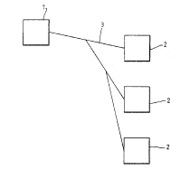
A TPON network comprises a head-end station 1, a
number of ter~in~tions 2, and a passive optical fibre
network 3 linking the head-end station l to the
t~rmin~tions 2. Although, for clarity, only three
terminations are shown, in practice many more
term;nations will be connected to a single head-end
station. Typically the head-end station is located in a
local telephone exchange and the terminations 2 are
subscriber stations in domesti~ or commercial premises or
street cabinets in the neighbourhood o~ the local
exchange.
The head-end station l broadcasts data over the
fibre network 3 as time division multiple access ~TDMA)
frames having a predetermined format. The frames include
control rh~nnels addressed to specific ones of the
term;nations 2 to control, amongst other parameters, the
SU~ TE SHE~T
WO g1 2 0 7 ~
/11867 PCT/GB91/~lO¢i;
amplitude and timing of the optical signals transmitted
onto the fibre network 3 by the terminations 2.
In the upstream direction, each termination 2
transmits data in a predetermined time slot, which data
is assembled into a TDMA frame at the head-end station l.
Since the TPON network is synchronous in operation it is
necessary to control the timing of the terminations both
to compensate for the different delays associated with
different positions of the terminations on the fibre
network 3 and to correct for any variation in the delay
and amplitude arising, for example, from local
fluctuations in the temperature of the network.
Figure lB shows the format of the return frame.
Traffic data is transmitted to the head-end station in 80
lS basic frames BFl... BF80. The basic frames BFl... BF80
are preceded by a header H which includes a phase-2
ranging sectïon R 720 bits long. Each termination 2 is
arranged to transmit onto the fibre network 3 a ranging
~it timed to arrive at a predetermined position within
the ranging section R. The head-end station l determines
the phase or each arriving ranging pulse and then
transmits control signals to the respective termination 2
to retard or advance the timing of the tr~n~m-~sion from
that termination 2 in order to ~;n;m;se the phase offset
between the received data from that termination and the
intended position of that data within the return frame
structure.
Figure 2 shows the structure of the head-end station
l. The incoming optical signals are received by an input
stage 4 which includes a conventional photo-electric
detector. The output from the input stage 4 is branched,
going both to a signal recovery stage 5 and to an A/D
sampler 6. The sampler 6 operates under the control of
the main CPU 7 to sample any selected portion of the
incoming signals. The output from the sampler 6 is
S~ lTE~
WO91/11867 2 0 7 ~ ~ ~ 3 PCT/GB91/00100
changed to a datastream of longer word--length and lower
bit-rate by a converter 8. The use of the sampler 6 is
described in greater detail i~ our co-pending unpublished
British application, no 8926548.2 entitled "Passive
5 -optical Network".
The signal recovery stage includes a data receiver
as shown in greater detail in Figure 3.
The serial data input stream is applied to a
serial-to-parallel converter ll. The output from the
lQ serial-to-parallel converter ll is communicated via an
8-bit wide data bus at a data rate of 2.56 M bytes/s.
In order to prevent readiwrite conflicts, two dual
port parallel line memory buffers (video line memories)
are provided for the control processor 12 which has DMA
access to both o~ the buffers. When data is being
written from the converter ll to a given one o~ the
bu~fers then a flag is set so that the processor reads
from the other of the buffers 13, 14.
An exchange interface is provided comprising an
8-bit wide FIFO arranged to provide eight parallel
exchange traf~ic output streams Tl... T8.
In use each inccming basic frame BF is broadcast
both to the control processor buffers 13, 14 and to the
exchange inter.ace 15. The operation of the buffers 13,
14 and the interface 15 is synchronised to the overall
frame structure and timed so that the control buffers
read only the control portion of each basic frame and the
exchange interface 15 reads only the traffic portion.
The appropriate enable signals are generated by a timing
unit locked to the exchange clock.
Qn the transmit side of the head-end station a
corresponding structure, shown in Figure 4 is used.
Control data 'rom the control processor 12' are fed via
buffers 13', 14' onto a parallel 8-bit bus. Traffic data
is fed onto the bus from an exchange interface 15'. On
SUBSTIl'UTE 51'11EF~
WO91/11867 ~ 0 7 ~ 3 3 PCT/~B91/00100
the output side of the bus a parallel-to-serial converter
11' forms a serial data stream. As on the recelve side,
the timing of the control processor buffers arld the
exchange inter ace ls synchronlsed to provlde traffic and
control data in the appropriate portions of each outgoing
basic frame BF. The bit order of the output frame is
scrambled using a scrambler S. A suitable scrambler is
described in the present applicant's earlier British
application no. 8727846, filed 27 November 1987.
Figures 5a-5g show timing diagrams for the enable
signals to the control buffers and the exchange
interface. Figure 5a shows the CPU interrupt which has
the same 10mS perlod as the received TDMA frames. Figure
5b shows the tlmlng of the bank switch whlch swltches
alternately between the two vldeo llne memories of the
data buffer ln the transmltter under the control of the
timing unit. Figure 5c shows the enabling signal for the
buf~er: the signal enables when it is low. It is timed
first to go low during the part of the header portion
corresponding to the phase-l ranging period.
Subseauently the buffer is enabled towards the end of
each basic frame in order to capture the control data
associated with that basic frame. As shown in Figure Sd,
the enabIe signal for the other of the video line
memories has the same structure but with a shift in phase
of one frame's length. The header portion is used for
system diagnostics. An encoded signal is transmitted
onto the fibre network and the state of the network may
be analysed using OTDR techni~ues.
Figures 5e-5g show the timing of the data receiver.
The structure is generally analogous to that used on the
transmit side, but with a phase offset of 250
microseconds corresponding to the loop delay for the
entire network system. The receive ~uffers when enabled
in the header portion capture phase-l ranging pulses, for
~UIB~~ LJTE S~EET
WO91/11867 ~ ~ 7
~ 3 PCT/GB91/001
_g ~
use in controlling the timing of transmissions from the
terminations, as described above.
3s
SlJ~ ulTE SHE T