Language selection

Search

Patent 2071556 Summary

Third-party information liability

Some of the information on this Web page has been provided by external sources. The Government of Canada is not responsible for the accuracy, reliability or currency of the information supplied by external sources. Users wishing to rely upon this information should consult directly with the source of the information. Content provided by external sources is not subject to official languages, privacy and accessibility requirements.

Claims and Abstract availability

Any discrepancies in the text and image of the Claims and Abstract are due to differing posting times. Text of the Claims and Abstract are posted:

  • At the time the application is open to public inspection;
  • At the time of issue of the patent (grant).
(12) Patent: (11) CA 2071556
(54) English Title: TDMA TRANSCEIVER CONTROLLER METHOD AND APPARATUS
(54) French Title: METHODE ET DISPOSITIF DE CONTROLE POUR EMETTEUR-RECEPTEUR AMRT
Status: Expired
Bibliographic Data
(51) International Patent Classification (IPC):
  • H04J 3/06 (2006.01)
  • H04B 7/212 (2006.01)
  • H04B 7/26 (2006.01)
(72) Inventors :
  • BINZEL, CHALES P. (United States of America)
  • DECLERCK, DANIEL J. (United States of America)
  • BUSSAN, CHRISTOPHER F. (United States of America)
(73) Owners :
  • MOTOROLA MOBILITY, INC. (United States of America)
(71) Applicants :
(74) Agent: GOWLING LAFLEUR HENDERSON LLP
(74) Associate agent:
(45) Issued: 1998-11-17
(86) PCT Filing Date: 1991-12-18
(87) Open to Public Inspection: 1992-06-21
Examination requested: 1992-06-11
Availability of licence: N/A
(25) Language of filing: English

Patent Cooperation Treaty (PCT): Yes
(86) PCT Filing Number: PCT/US1991/009588
(87) International Publication Number: WO1992/011715
(85) National Entry: 1992-06-11

(30) Application Priority Data:
Application No. Country/Territory Date
632,236 United States of America 1990-12-20

Abstracts

English Abstract


A radio transceiver (119) including a transmitter (111), a
receiver (107), and a controller (113). The controller (113)
creates a fixed period reference signal (201) and a second
reference signal (203) which has a variable delay in time from
the fixed period reference signal (201). In addition the
controller (113) creates a plurality of control signals used to
control parts of the transceiver (119) and which are time
dependant upon the second reference signal 203). Therefore,
the adjusting of the variable delay of the second signal
subsequently adjusts the plurality of control signals.


French Abstract

L'invention est un émetteur-récepteur radio (119) qui comprend un émetteur (111), un récepteur (107) et un contrôleur (113). Le contrôleur (113) produit un signal de référence de période fixe (201) et un second signal de référence (203) à retard variable par rapport au signal de référence à période fixe (201). Le contrôleur (113) produit également une pluralité de signaux de commande qui sont utilisés pour commander divers éléments de l'émetteur-récepteur (119) et qui sont asservis temporellement au second signal de référence (203). On peut par conséquent ajuster la pluralité de signaux de commande en ajustant le retard variable du second signal.

Claims

Note: Claims are shown in the official language in which they were submitted.


WHAT IS CLAIMED IS:

1. A method of controlling the timing of a TDMA (time division multiple access)
transceiver, the transceiver including a transmitter, a receiver, and a controller, the
method comprising the steps of:
creating a first reference signal having a first fixed period;
creating a second reference signal having a second fixed period and a variable
delay in time from said first reference signal,
creating a plurality of control signals having fixed delays in time from said
second reference signal; and
adjusting said second reference signal's variable delay in time, such that said
plurality of control signals are adjusted in time.

2. A method of controlling the timing of a Time Division Multiple Access
(TDMA) transceiver, the transceiver including a transmitter, a receiver, a controller,
and a microprocessor each disposed within a radiotelephone, the method comprising
the steps of:
creating a first reference signal with a fixed period in the controller;
creating a second reference signal having a second fixed period and a variable
delay in time from said first reference signal in the controller;
creating, in the controller, a first control signal having a first fixed delay in
time from said second reference signal, such that the receiver is programmed to
receive a first radio frequency for a duration of time determined by an assertion time
value;
creating, in the controller, a second control signal having a fixed delay in time
from said first control signal, during which the receiver acquires data;
programming the controller from the microprocessor such that said first
control signal has a second fixed delay in time from said second reference signal;
programming the controller from the microprocessor such that said assertion
time value has a second time value;


creating, in the controller, a third control signal having a variable delay in time
from said second reference signal, such that the digital modulator is activated;creating, in the controller, a fourth control signal having a fixed delay in time
from said second reference signal, such that the transmitter is activated;
creating, in the controller, said first control signal having said second fixed
delay in time from said second reference signal, such that, the receiver is programmed
to receive a second radio frequency for a duration of time determined by said assertion
time value;
programming the controller from the microprocessor such that said first
control signal has said first fixed delay in time from said second reference signal;
programming the controller from the microprocessor such that said assertion
time has a first time value,
programming the controller from the microprocessor such that said second
reference signal has a second variable delay in time,
programming the controller from the microprocessor such that said third
control signal has a second variable delay in time; and
creating, in the controller, said second control signal a second time having said
fixed delay in time from said first control signal, said first control signal having said
second fixed delay in time.

3. A method of controlling the timing of a Time Division Multiple Access
(TDMA) transceiver in accordance with claim 1, wherein said first clock signal is the
master frame reference signal and said second clock signal is the channel frame
reference signal.

4. A TDMA (time division multiple access) radio system including at least a first
and a second fixed-site transceiver, a first remote transceiver, said TDMA radiosystem comprising:
first means for communicating between the first fixed-site transceiver and the
first remote transceiver, said first means for communicating having a first propagation
delay;


11

second means for communicating between the second fixed-site transceiver
and the first remote transceiver, said second means for communicating having a
second propagation delay; and
a timing controller disposed within the first remote transceiver comprising:
first means for generating a first clock signal,
second means for generating a second clock signal synchronized to said first
clock signal and having a reconfigurable fixed delay from said first clock signal
related to said first propagation delay,
third means for generating a plurality of control signals having fixed delays intime from said second clock signal, and
means for reconfiguring said reconfigurable fixed delay responsive to said
second propagation delay during communications between the first remote transceiver
and the second fixed-site transceiver.

5. A time division multiple access (TDMA) radio system in accordance with
claim 4 wherein said means for reconfiguring is further responsive to changes in said
first propagation delay during communications between the first remote transceiver
and the first fixed-site transceiver.

6. A method of controlling the timing of a Time Division Multiple Access
(TDMA) transceiver, the transceiver including a transmitter, a receiver, and a
controller, the method comprising the steps of:
creating a first clock signal having a fixed period, wherein said fixed period
does not exceed nine (9) milliseconds,
creating a second clock signal synchronized to said first clock signal and
having a reconfigurable fixed delay from said first clock signal;
creating a plurality of control signals having fixed delays in time from said
second clock signal; and
reconfiguring said second clock signal's fixed delay in time, such that said
plurality of control signals are adjusted in time.


12

7. A method of controlling the timing of a Time Division Multiple Access
(TDMA) transceiver in accordance with claim 6 wherein said fixed period is equal to
4.615 milliseconds.

8. A method of controlling the timing of a TDMA transceiver in accordance with
claim 1 wherein said first and said second fixed periods are equal to 4.615
milliseconds.

Description

Note: Descriptions are shown in the official language in which they were submitted.


207 1~;~5 ~


TDMA Transceiver Controller Method and
Apparatus

l O
Field of the Invention

This invention generally relates to Time Division Multiple
Access (TDMA) communication systems and more specifically
15 relates to controllers for transceivers contained within a
TDMA communication system.

Background of the Invention

2 0 In a TDMA communication system, a given radio
frequency ch~nnel is divided into multiple time slots. A given
transceiver in a TDMA communication system is assigned
specific timeslots on which it can broadcast and specific
timeslots during which desired information can be received.
2 5 This requires the transmitter and receiver to be turned on and
off at different times.
In a digital telephone system, such as the system specified
by the Group Special Mobile (GSM) committee, there is a
requirement for the mobile transceivers to maintain
3 0 synchronization to multiple fixed site transceivers. The mobile

~7~6


transceiver must track the shift in time relative to each fixed
site transceiver with which it maintains synchronization. The
GSM digital telephone system is also required to monitor the
power levels of adjacent fixed site transceivers so it can change
5 to the best fixed site transceiver when the signal strength of the
current fixed site transceiver dwindles. These requirements
generate a need for a complex set of sign~ls to allow the
transceiver hardware to switch quickly between radio
frequencies of different fixed site receivers and~ to adapt quickly
I O to time shifts of each fixed site transceiver.
Generally, complex sets of control sign~ls have been
generated in the past with use of complex specialized
hardware with software maint~ining the control sign~ls. The
software required a significant amount of calculations prior to
15 generation of each signal and a significant amount of
intervention with the specialized hardware. Typically, in
technology today there is a need for reduction in size, power
consumption and cost, this need is m~gnified in a portable or a
mobile digital telephone because of the increased amount of
2 0 circuitry required over a standard portable or mobile analog
radiotelephone. Therefore, a need exists for a transceiver
controller which can fulfill the complex requirements of
operating in a TDMA communication systems environment
with a minim~l amount of software intervention from a
2 5 microprocessor. This will free up space for other
computations in the microprocessor and will ultimately
reduce the size and cost of the communication device.

2Q71~ 6


s~mm~ry of the Invention

The present invention encompasses a method and
5 apparatus for controlling a radio transceiver including a
transmitter, a receiver, and a controller. The controller
creates a fixed period reference signal and a second reference
signal which has a variable delay in time from the fixed period
reference sign~l. In addition the controller creates a plurality
1 0 of control si~n~ used to control parts of the transceiver and
which are time dependent upon the second reference siEn~l.
Therefore, the adjusting of the variable delay of the second
signal subsequently adjusts the plurality of control signals.

1 5Brief Description of the Drawings

FIG. 1 is a block diagram of a radio frequency
transmission system.
FIG. 2 is a timing diagram of the control signals utilized
2 0 in a transceiver which may employ the present invention.
FIGS. 3A and 3B are a flowchart of the process used by a
transceiver controller which may employ the present
invention.

2 5Description of a Preferred Embodiment

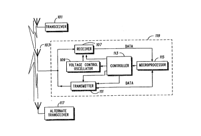
FIG.1 shows a block diagram of a TDMA radio
communications system, such as an European digital
radiotelephone system specified by the Group Special Mobile
3 0 (GSM) committee. The system is essentially comprised of one

2 ~ 7 ~


serving fixed site transceiver 101, one alternate fixed site
transceiver 117 and a mobile or portable transceiver 119. The
mobile or portable transceiver 119, hereinafter be referred to as
the remote transceiver 119, is contained within a digital
radiotelephone as specified by the GSM committee. The
serving fixed site transceiver 101 uses at least one specified
radio frequency (RF) channel divided into at least eight
timeslots to communicate with the remote transceiver 119 and
other remote transceivers which are within the serving range
1 0 of the serving fixed site transceiver 101. The remote
transceiver 119 monitors the power levels of all of the alternate
fixed site transceivers within a given area including the
alternate fixed site transceiver 117. The remote transceiver 119
also remains synchronized with six adjacent fixed site
transceivers. The synchronization is maintained and the
power measurements are taken so when the remote
transceiver 119 needs to switch to another fixed site transceiver
it can choose the best alternate fixed site transceiver 117 and
switch to the alternate fixed site transceiver 117 without losing
2 0 desired data.
The remote transceiver 119 contains a receiver 107, a
transmitter 111, a voltage controlled oscillator (VCO) 109, a
transceiver controller 113 and a microprocessor 115, the
microprocessor 115 and the controller 113 can be integrated
2 5 into a microcontroller such as a MC68332 available from
Motorola, Inc. The receiver 107 is responsible for
demodulating RF sign~l~ received by the antenna 103 from
multiple fixed site transceivers 101, 117 having multiple
carrier frequencies. The VCO 109 is responsible for adjusting
3 0 its output frequency to the desired carrier frequency which the

21~71~


receiver 107 needs to receive. Data from the digital
radiotelephone is input into the transmitter 111 to be sent to the
serving fixed site transceiver 101. The transmitter 111 digitally
modulates the data with the appropriate carrier frequency,
5 ~mplifies the data and sends it to the serving fixed site
transceiver 101 via the ~ntenn~ 103.
The controller 113 and the microprocessor 115 work
together to m~int~in synchronization between the remote
transceiver 119 and the fixed site transceivers 101, 117, and
l 0 control the internal timing to transmit and receive data.
FIG.2 reveals the timing of the control si~n~ls involved. First,
the controller 113 creates a master frame reference signal 201.
The m~ster frame reference signal 201 has a period of 4.615
mS, this signal is the fixed reference signal from which all
l 5 other control and reference signals are based.
For each fixed site transceiver 101, 117 that the remote
transceiver 119 is synchronized to there is a channel frame
reference signal 203. The channel frame reference signal 203
is the reference signal to which all subsequent control sign~ls
2 0 for an individual ch~nnel reference themselves. The delay
between the channel frame reference signal 203 and the
master frame reference signal 201 is adjusted once during
each period of the master frame reference signal 201 for
changes in propagation delay of the RF signals transmitted
2 5 and received between the remote transceiver 119 and the
serving fixed site transceiver 101.
The RF'START control signal 205 has two fixed delay times
from the channel frame reference signal 203, the first fixed
delay time ( 310 uS) is the length of time until receiving the
3 0 data from the serving fixed site transceiver 101, the second

2~


fixed delay time (3.5 mS) is the length of time until measuring
the signal strength of an adjacent fixed site transceiver 117.
The length of time that the RFSTART control signal 205 is
asserted is not pertinent to the design, therefore, no
5 microprocessor 115 computations are necessary to create this
control sign~l. The changes in the timing are controlled by the
changes made to the channel frame reference signal 203. The
RFSTART control signal 205 precedes the RXACQ control
signal 207 and functions as a preparation signal to the receiver
I 0 section loading the synthesizer and the automatic gain control
(AGC) level information into the receiver. The RXACQ control
signal 207 follows the RFSTART control signal 205 by the worst
case locking time of the synthesizer, 818 uS. The length of time
RXACQ control signal 207 is asserted is the length of time that
1 5 the receiver processes the received RF si n~l~ via the antenna
103. There are two different assertion times for the RXACQ
control signal 207 in this embodiment, the first time (607 uS) is
the length to receive one timeslot of data from the serving fixed
site transceiver 101, the second time (237 uS) is the length to
2 0 receive enough information to determine the signal strength of
an adjacent fixed site transceiver 117.
The DMCS control signal 213 is used to begin the digital
modulator in the transmitter 111 prior to a tr~n~mission of
data to the serving fixed site transceiver 101. The delay of the
2 5 DMCS control signal 213 is referenced to the channel frame
reference signal 203 and is different for each fixed site
transceiver. The fixed site transceiver sends the remote
transceiver 119 the delay information prior to tr~n~mi~sion.
This delay is programmed into the controller 113 by the
3 0 microprocessor 115. The DMCS control signal 213 is asserted

~Q73L~ ~


(650 uS) prior to, during and after the tr~n~mi.~sion period of
the transmitter 111. The TXKEY control signal 215 determines
the length of the tr~n~mi~Sion period, 577 uS. The TXKEY
control signal has a fixed delay of 37.1 uS from the asserting
5 edge of the DMCS control signal 213, this fixed delay is the
worst case time for the transmitter to adjust properly.
These timing of the si~n~ql.c are specific to the hardware
chosen for the design, and a person of average skill in the art
would appropriately adjust these times for their design.
l 0 There are two interrupts necessary for the microprocessor
115 to program the controller 113 for proper operation of the
remote transceiver 119. The first interrupt 211 sets the proper
time delay between the master frame reference signal 201 and
the chP.nnel frame reference 203, sets the delay between the
ch~nnel frame reference 203 and RFSTART control signal 205
to the first fixed delay and the RXACQ control signal assertion
time to the first fixed time for receiving the data from the
serving fixed site transceiver 101. The second interrupt 209
sets RFSTART control signal 205 to the second fixed delay and
2 0 the RXACQ control signal assertion time to the second fixed
time for measuring the signal strength of the adjacent fixed
site transceiver 117.
FIG. 3 is a flow chart of the process used by the controller
to effectively control the remote transceiver 119. First, the
2 5 master frame reference signal 201 is created at 303. The
channel frame reference signal 203 is created at 305. Next, the
RFSTART control signal 205is created to set up the receiver
107 for att~ining RF sign~l~ from the serving fixed site
transceiver 101 at 307. At 309, the RXACQ signal 207is
3 0 asserted for acquiring the RF signals. The microprocessor is


~ ~ 7 ~ 5 5 ~

then interrupted to program the controller for measuring the
signal strength of the adjacent fixed site transceiver 117. First,
it sets the delay between the channel frame reference signal
203 and RFSTART control signal 205 at 311, followed by setting
5 the RXACQ control signal assertion time to the second fixed
time at 313. The DMCS control signal 213 is asserted for the
entire tr~n~mission period at 315 and 'l'2~K~;Y control signal
215 is asserted 37.1uS later at 317. Next, the RFSTART control
signal 205 is created to set up the receiver 107 for measuring
I 0 the signal strength from the adjacent fixed site transceiver 117
at 319. The microprocessor 115 is then interrupted to program
the controller 113 for receiving data from the serving fixed site
transceiver 101. First, the microprocessor 115 sets the delay
between the channel frame reference signal 203 and RFSTART
1 5 control signal 205 at 321, followed by setting the RXACQ control
signal assertion time to the first fixed time at 323. Then the
microprocessor 115 adjusts the delay between the master
frame reference signal 201 and the channel frame reference
signal 203 at 325. At 327, the microprocessor 115 adjusts the
2 0 time delay between the channel frame reference signal 203 and
the DMCS control signal 213. The controller 113 then creates
the RXACQ signal to measure the signal strength of the
adjacent fixed site transceiver 117. The program then repeats.


Representative Drawing
A single figure which represents the drawing illustrating the invention.
Administrative Status

For a clearer understanding of the status of the application/patent presented on this page, the site Disclaimer , as well as the definitions for Patent , Administrative Status , Maintenance Fee  and Payment History  should be consulted.

Administrative Status

Title Date
Forecasted Issue Date 1998-11-17
(86) PCT Filing Date 1991-12-18
(85) National Entry 1992-06-11
Examination Requested 1992-06-11
(87) PCT Publication Date 1992-06-21
(45) Issued 1998-11-17
Expired 2011-12-18

Abandonment History

There is no abandonment history.

Payment History

Fee Type Anniversary Year Due Date Amount Paid Paid Date
Application Fee $0.00 1992-06-11
Registration of a document - section 124 $0.00 1993-01-26
Maintenance Fee - Application - New Act 2 1993-12-20 $100.00 1993-09-28
Maintenance Fee - Application - New Act 3 1994-12-19 $100.00 1994-09-26
Maintenance Fee - Application - New Act 4 1995-12-18 $100.00 1995-09-28
Maintenance Fee - Application - New Act 5 1996-12-18 $150.00 1996-09-24
Maintenance Fee - Application - New Act 6 1997-12-18 $150.00 1997-09-19
Final Fee $300.00 1998-07-03
Maintenance Fee - Application - New Act 7 1998-12-18 $150.00 1998-09-25
Maintenance Fee - Patent - New Act 8 1999-12-20 $150.00 1999-11-04
Maintenance Fee - Patent - New Act 9 2000-12-18 $150.00 2000-11-03
Maintenance Fee - Patent - New Act 10 2001-12-18 $200.00 2001-11-02
Maintenance Fee - Patent - New Act 11 2002-12-18 $200.00 2002-11-04
Maintenance Fee - Patent - New Act 12 2003-12-18 $200.00 2003-11-05
Maintenance Fee - Patent - New Act 13 2004-12-20 $250.00 2004-11-04
Maintenance Fee - Patent - New Act 14 2005-12-19 $250.00 2005-11-04
Maintenance Fee - Patent - New Act 15 2006-12-18 $450.00 2006-11-07
Maintenance Fee - Patent - New Act 16 2007-12-18 $450.00 2007-11-07
Maintenance Fee - Patent - New Act 17 2008-12-18 $450.00 2008-11-12
Maintenance Fee - Patent - New Act 18 2009-12-18 $450.00 2009-11-10
Maintenance Fee - Patent - New Act 19 2010-12-20 $450.00 2010-11-17
Registration of a document - section 124 $100.00 2011-12-16
Owners on Record

Note: Records showing the ownership history in alphabetical order.

Current Owners on Record
MOTOROLA MOBILITY, INC.
Past Owners on Record
BINZEL, CHALES P.
BUSSAN, CHRISTOPHER F.
DECLERCK, DANIEL J.
MOTOROLA, INC.
Past Owners that do not appear in the "Owners on Record" listing will appear in other documentation within the application.
Documents

To view selected files, please enter reCAPTCHA code :


To view images, click a link in the Document Description column. To download the documents, select one or more checkboxes in the first column and then click the "Download Selected in PDF format (Zip Archive)" or the "Download Selected as Single PDF" button.

List of published and non-published patent-specific documents on the CPD .

If you have any difficulty accessing content, you can call the Client Service Centre at 1-866-997-1936 or send them an e-mail at CIPO Client Service Centre.


Document
Description 
Date
(yyyy-mm-dd) 
Number of pages   Size of Image (KB) 
Cover Page 1998-10-26 1 46
Cover Page 1994-04-16 1 18
Abstract 1994-04-16 1 21
Claims 1994-04-16 8 164
Drawings 1994-04-16 4 149
Description 1994-04-16 8 327
Description 1997-11-12 8 321
Claims 1997-11-12 4 139
Representative Drawing 1998-10-26 1 8
Correspondence 1998-07-03 1 34
International Preliminary Examination Report 1992-06-11 24 699
Prosecution Correspondence 1997-09-04 2 50
Office Letter 1993-02-09 1 29
Examiner Requisition 1997-03-11 2 80
Assignment 2011-12-16 8 368
Fees 1996-09-24 1 97
Fees 1995-09-28 1 94
Fees 1994-09-26 2 203
Fees 1993-09-28 1 90