Note: Descriptions are shown in the official language in which they were submitted.
~- 2071~8~
1 1182-12
STRUCTURE OF A CERAMIC FILTER
The invention relates to a dielectric filter which comprises
a body of a dielectric material having upper and lower sur-
faces, two side surfaces, two end surfaces and at least one
hole which extends from the upper surface to the lower sur-
face, and an electrically conductive layer covering major
portions of the lower surface, one side surface, both end
surfaces and the surface of said hole thereby forming a
transmission line resonator, the uncoated side surface
having an electrode pattern thereon for providing electrical
signal coupling to and from the transmission line resonator.
Finally, at least the patterned surface is covered with a
cover made of a conductive material, whereupon the di-
electric filter is enveloped by a conductive layer substan-
tially throughout. A filter of this type is described in
European Patent Application EP-A-0401839 and corresponding
US Patent No. 5103197.
The dimensioning of the cover and forming it to the correct
size and shape constitutes a precise and time-consuming work
step, and the manufacturing of the cover is a cost-increa-
2S sing factor. Furthermore, the mechanical fastening of thedimensioned cover to the ceramic block is cumbersome and
slow. The final step of manufacture of a ceramic filter thus
substantially increases the cost of manufacture of the
filter.
According to the present invention, there is provided a
filter comprising a body of dielectric material having an
upper surface, a lower surface, two side surfaces, two end
surfaces and at least one hole which extends from the upper
surface to the lower surface and an electrically conductive
layer covering major portions of the lower surface, one side
surface, both end surfaces and the surface of said hole
thereby forming a transmission line resonator, the uncoated
~: ,
:~
- 2~7158~
side surface having an electrode pattern thereon for
providing electrical signal coupling to and from the trans-
mission line resonator characterized in that the two
opposing end surfaces extend beyond the patterned side sur-
face to provide first and second parallel flanges enclosingthe patterned side surface on two sides for mounting said
filter on a substrate such that the substrate is substan-
tially parallel to and spaced from the patterned side sur-
face. This has the advantage that the expensive final step
of manufacturing and filtering a formed cover is eliminated.
This reduces the manufacturing costs as this slow manu-
facturing step is eliminated and there is the saving on the
cost of manufacturing the cover as no cover for the
patterned side surface is required since this is provided by
the base to which the filter is fastened.
The invention will now be described, by way of example only,
with reference to the accompanying drawings, of which:
,
Figure 1 shows a first embodiment of a filter body of the
invention;
Figure 2 shows a second embodiment of a filter body of the
invention;
Figure 3 shows a third embodiment of a filter body of the
invention; and
Figure 4 shows a filter body fastened to a substrate.
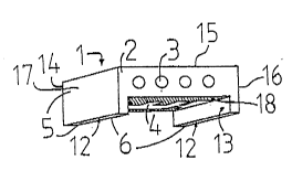
As with the known filters described above, a filter 1
according to the invention comprises a body of dielectric
material e.g. a ceramic material which has parallel holes 3
extending from an upper surface 2 to a lower surface 14 so
as to constitute transmission-line resonat~rs. All of the
surfaces of the body including the holes 3, with the
exception of the upper surface 2 and a patterned side sur-
face 4 which has electrode patterns thereon as in the known
~ ' .
.
-- 2071~8~
filter are coated throughout with an electrically conductive
material 5. The coated inner surfaces of the holes 3 connect
with the coating of the lower surface 14. The coupling from
and between the resonators is by means of the electrode
patterns 18 formed on the side surface 4 using a mask, these
electrode patterns 18 being indicated in Figure 1 by
hatching. The number, shape and properties of the electrode
patterns 18 and any discrete components connected thereto
vary according to the desired properties of the filters and
are of no particular relevance to the present invention and
will so not be described here. They are, however, described
in EP-A-0401839.
The two opposing end faces (16, 17) of the body extend
beyond the patterned side surface 4 to provide two flanges
6 between which is the patterned side surface 4. These
flanges 6, which are perpendicular to the patterned side
surface 4 and extend to the same distance, are formed at the
manufacturing stage of the ceramic block, being thus
integral with the body, and an extra manufacturing step is
not needed. The flange surface integral with the upper
surface is uncoated, but the inner surface 13 may be coated
or uncoated. The flange surface 12 parallel to the patterned
side surface 4 is coated.
In a second embodiment shown in Figure 2, the lower surface
14 is also extended beyond the patterned side surface 4 to
the same distances as the two parallel flanges 6 to provide
a third flange 7, which is also perpendicular to the
patterned side surface 4 and integral with the body.
Additionally, the two parallel flanges 6 extend beyond the
upper surface 2 by the same distance so that the upper
surface 2 is between the two parallel flanges 6 and the
coated side surface opposite the patterned side surface 4
extends beyond the upper surface 2 to the same extent as the
two parallel flanges 6 to provide a fourth flange 8. In this
embodiment, both the upper surface 2 and the patterned side
surface 4 are enclosed on three sides. All of the inner sur-
- 2071~8~
faces of these flanges 6 and 8 adjacent the upper surface 2
may be coated with a conductive material, and a cover made
of a conductive material can be fastened to the flanges 6
and 8 to cover the upper surface 2. The third flange 7,
which extends from the lower surface 14, may also be coated
on all sides with a conductive material. The inner surfaces
13 of the flanges 6, 7 and 8 may be left uncoated. When a
cover is provided it may additionally have, above the reson-
ators, tongues for regulating the resonance frequency.
In a third embodiment shown in Figure 3, the holes 3 are
located in cylindrical recesses 11. The surfaces of the
recesses 11 are uncoated, so that the recesses form an air
clearance above the resonators when the upper surface 2 is
provided with a cover made of a conductive material, which
cover may have, above the resonators, tongues by the bending
of which the resonance frequency can be regulated.
The completed filter of any of the three embodiments is
fastened, as shown in Figure 4, with the patterned side sur-
face 4 downwards, to a base 9, for example a circuit board
or a metal sheet, which has, at least on one side, a con-
ductive material over an area the size of the filter, this
material being in electrical contact with the coated sur-
faces of the filter 1. Thus the filter is enveloped by aconductive layer on substantially all sides. The fastening
of the filter 1 to the base 9 is carried out so that signal
conductor pins 10 for connection to the patterned side sur-
face 4 enter via holes in the base so that they are insu-
lated from the conductive layer of the base, and thereafterthe first, second and third flanges 6 and 7 are soldered to
the base 9 by the electrically conductive coating.
If there is no third flange 7 at the end of the lower edge
of the patterned side, the opening left below the lower
surface can be covered with a cover made of a conductive
material. If the opening is not covered, the filter should
be placed sufficiently far from other nearby components so
,
,
' ~ ~
--- 2071~8~
that they will not cause interference in the operation of
the dielectric filter.
The upper surface 2 of any of the three embodiments may also
be provided with a cover of a conductive material (not
shown). The cover may be provided with tongues located above
the resonator holes 3 which can be bent to tune the reson-
ator to the required resonator frequency. The provision of
such tongues is well known in filter technology. If no cover
is provided, the filter should be placed sufficiently far
from other components to avoid interference which will
effect the operation of the filter.
Instead of conductor pins 10, the wiring can be implemented
by bringing from the surface 4 conductors as conductor
strips via the inner surface 13 of first, second and third
flanges 6 or 7 to the flange surface 12 which will lie on
the base, whereupon they can be soldered to the conductor
spots (not shown) on-the base.
It will be evident to a person skilled in the art, from the
foregoing description, that variations are possible within
the scope of the present invention.
: ~ . . -