Note: Descriptions are shown in the official language in which they were submitted.
~71~2~
FREQUENCY DISCRIMINATOR AND HETERODYNE RECEIVER
PROVIDED WITH THE FREQUENCY DISCRIMINATOR FOR
COHERENT LIGHTWAVE COMMUNICATIONS
BACKGROUND OF THE INVENTION
Field of the Invention
The present invention generally relates to a
frequency discriminator for converting an input signal
to a DC voltage or a DC current at the level
corresponding to the frequency or average frequency of
the input signal and, more particularly, to a frequency
discriminator having high accuracy in frequency
identification and a wide capture range. The invention
further relates to application of the frequency
discriminator to a heterodyne receiver for coherent
lightwave communications.
Description of the Related Art
The coherent lightwave communications system
has improved reception sensitivity by 10 to 20dB over
conventional intensity modulation/direct detection
(IM/DD) and facilitates optical frequency-division
multiplex. Therefore, the system is expected to be put
- ~07162~1
to practical use in high speed and long distance
transmission. In the heterodyne receiver for coherent
lightwave communications, a local light beam is mixed
with a signal light beam received and the mixed light
beams are optically detected by a photodiode having a
square-law detection characteristic and thereby an
intermediate-frequency signal is obtained. The
intermediate-frequency signal is demodulated to a
baseband signal. Since the frequency of the
intermediate-frequency signal corresponds to the
difference between the frequency of the signal light and
the frequency of the local light, if the center
frequency of the signal light and/or the local light is
varied by changes in ambient conditions or the like, the
center frequency of the intermediate-frequency signal is
also varied. A variation in the center frequency of the
intermediate-frequency signal hinders normal
demodulation. Therefore, in the heterodyne receiver,
automatic frequency control (AFC) is generally performed
to keep the center frequency of the intermediate-
frequency signal constant.
In practicing AFC, a frequency discriminator
is used. The frequency discriminator applied to AFC in
the heterodyne receiver converts the input intermediate-
2 ~ 2 ~
frequency signal to a DC voltage at the levelcorresponding to the center frequency of the input
intermediate-frequency signal and outputs the DC
voltage. Frequency discriminators of the described type
are required to have the following characteristics:
(A) That accuracy in frequency identification
is high. In other words, that the output voltage level
greatly varies with a change in the frequency. As the
accuracy in frequency identification is increased,
frequency stability in the automatic frequency control
is improved.
(B) That the range of frequencies for which
automatic frequency control can be achieved by a control
loop (capture range) is wide.
There has so far been known a frequency
discriminator, in which it is adapted such that an input
signal to be subjected frequency discrimination is
divided into two signals, one of the divided signals is
given a predetermined delay time, and this signal is
mixed with the other of the divided signals and the
mixed signal is output.
In such prior art frequency discriminator,
there exists a trade-off between improvement of the
accuracy in the frequency identification and expansion
of the capture range, namely, lt ls lmposslble to satisfy both
requirements at the same time.
SUMMARY OF THE INVENTION
Accordlngly, an ob~ect of the present lnvention is
to provide a frequency dlscrlmlnator wlth both hlgh accuracy
ln frequency ldentlflcatlon and a wlde capture range.
Another ob~ect of the present lnventlon is to
provlde a hlgh-performance heterodyne recelver for coherent
lightwave communications using the frequency discrimlnator.
Accordlng to an aspect of the present lnventlon
there ls provlded a frequency dlscrlminator comprising:
a delay clrcult arranged to delay an lnput slgnal by a
predetermined delay tlme~ and to output the delayed slgnal,
wherein the delay time ~ is chosen such that it satlsfles the
condltlon given by
fIF = (2n + 1)/4~,
where n is a positive integer;
a filter arranged to recelve sald lnput slgnal to be
sub~ected to frequency dlscrlmlnatlon;
a branch clrcult adapted to dlvlde an lnput slgnal lnto
two slgnals and to provlde the two signals to flrst and second
output ports, sald branch clrcult having an lnput port
operatlvely connected wlth an output port of sald fllter, said
first output port of sald branch clrcuit being operatlvely
connected wlth an input port of sald delay circult;
a mlxer operatively connected wlth sald second output
port of said branch circult and an output port of sald delay
clrcuit for mixing the slgnal from sald branch clrcult and the
-- 4
28170-47
~; 2
signal from said delay clrcult; and whereln said fllter is
elther
a hlgh-pass fllter havlng a cut-off frequency, denoted by
fHPF, whlch satlsfles the condltlon glven by
fHPF = (2n - 1)/4~ ; or
a low pass fllter havlng a cut-off frequency, denoted by
fLPF, whlch satlsfles the condltlon glven by
fLPF = (2n + 3)/4~; or
a bandpass fllter havlng a cut-off frequency on the hlgh
frequency slde and a cut-off frequency on the low frequency
slde of sald bandpass fllter, denoted by fH and fL,
respectlvely, whlch satlsfy the condltlons glven by
fH = (2n ~ 3)/4 ~,
fL = (2n - 1)/4~ .
The above and other ob~ects, features and advantages
of the present lnventlon and the manner of realizlng them will
become more apparent, and the inventlon ltself wlll best be
understood from a study of the followlng descrlptlon and
appended clalms with reference to the attached drawlngs
showlng some preferred embodlments of the lnventlon.
BRIEF DESCRIPTION OF THE DRAWINGS
FIG. 1 ls a block dlagram showlng a prlor art
28170-47
.
2 ~
example of frequency discriminator;
FIG. 2 is a graph showing a frequency
discrimination characteristic of the frequency
discriminator shown in FIG. l;
FIG. 3 is a block diagram showing a first
embodiment of the frequency discriminator according to
the present invention;
FIG. 4A, FIG. 4B, and FIG. 4C are drawings
explanatory of characteristics of the frequency
discriminator shown in FIG. 3;
FIG. 5 is a block diagram showing a second
embodiment of the frequency discriminator according to
the present invention;
FIG. 6A, FIG. 6B, and FIG. 6C are drawings
explanatory of characteristics of the frequency
discriminator shown in FIG. 5;
FIG. 7 is a block diagram showing a third
embodiment of the frequency discriminator according to
the present invention;
FIG. 8A, FIG. 8B, and FIG. 8C are drawings
explanatory of characteristics of the frequency
discriminator shown in FIG. 7;
FIG. 9A and FIG. 9C are drawings showing
actually measured values of characteristics of the
2~7~L~2 r~
frequency discriminator of FIG. 1 and FIG. 7,
respectively, when a sine wave signal is input thereto;
FIG. 9B is a drawing showing actually measured
value of the characteristic of a bandpass filter;
FIG. 10 is a drawing showing actually measured
values of a frequency discrimination characteristic of
the frequency discriminator of FIG. 7 when an
intermediate-frequency signal with modulated components
is input thereto;
FIG. 11 is a block diagram showing an improved
example of the frequency discriminator of FIG. 7;
FIG. 12 is a block diagram showing another
improved example of the frequency discriminator of FIG.
7;
FIG. 13 is a graph for comparison of measured
frequency discrimination characteristics of the
frequency discriminator of FIG. 12 when an AGC circuit
is operated and not operated; and
FIG. 14 is a block diagram of a heterodyne
receiver for coherent lightwave communications with the
frequency discriminator of the present invention applied
thereto.
DESCRIPTION OF THE PREFERRED EMBODIMENTS
2~7~2 ~
In understanding the embodiment of the present
invention, it is considered helpful to understand
structure and operation of a prior art frequency
discriminator, and therefore explanation of the same
will be made first. FIG. 1 is a block diagram showing
an example of a prior art frequency discriminator. The
frequency discriminator comprises a branch circuit 2 for
dividing a signal such as an intermediate-frequency
signal to be subjected to frequency discrimination, a
delay circuit 4 for giving a predetermined delay of time
~ to one of the signals divided by the branch circuit 2
and outputting the delayed signal, and a mixer 6 for
mixing the output signal from the delay circuit 4 and
the other of the divided signals by the branch circuit 2
and outputting the mixed signal.
When the signal input to the frequency
discriminator is expressed as cos2~ ft (f: frequency, t:
time), the output voltage Vo of the frequency
discriminator is expressed as
Vo = cos2~ ft cos2~ f(t - ~ )
= (1/2)cos2~ f~ + (1/2)cos2~ f(2t - T ) . . ~ (I )
By extracting the DC component corresponding
to the first term of the right side using a suitable
low-pass filter, a frequency discrimination
,~a
2~7~2~
characteristic as shown in FIG. 2 can be obtained.
Referring to the graph shown in FIG. 2, the axis of
ordinates represents the output voltage of the frequency
discriminator and the axis of abscissas represents the
frequency. The reason why there is shown a region in
which the frequency is negative is that we are
considering the frequency of the intermediate-frequency
signal as the frequency in question and that the
frequency of the intermediate-frequency signal can take
on both positive values (real) and negative values
(image) depending on which is the larger of the
frequency of the signal light and the frequency of the
local light.
In the operation of an AFC with the use of the
frequency discriminator having a frequency
discrimination characteristic as shown in FIG. 2, when
the output voltage of the frequency discriminator is
positive, the frequency of the local light is varied in
the direction to increase the center frequency of the
intermediate-frequency signal, whereas, when the output
voltage of the frequency discriminator is negative, the
frequency of the local light is varied in the direction
to decrease the center frequency of the intermediate-
frequency signal. As a result, the center frequency of
2~7~2~
the intermediate-frequency signal is converged on the
point where the output voltage level of the frequency
discriminator becomes zero. If the center frequency of
the intermediate-frequency signal is within the capture
range, one frequency stabilization point can be
obtained. When the center frequency of an intermediate-
frequency signal is outside the capture range, the
stabilization point is obtained at a point where the
frequency is higher or lower than that in the desired
frequency stabilization point.
To be concrete, denoting the center frequency
of an intermediate-frequency signal by fIF, the center
frequency fI F iS stabilized so as to satisfy this
expression
fI F = ( 2n + 1)/4~ (n = 0, 1, 2, .. ). ~-- (2)
Conversely speaking, the delay time r is set up
according to the frequency to be stabilized, such that
the expression (2) is satisfied.
In order to widen the capture range in the
frequency discriminator shown in FIG. 1, it is
advantageous to decrease the value of n in the
expression (2) and reduce the delay time ~ ,
accordingly. For example, when the center frequency fI F
of an intermediate-frequency signal is set up at the
2 ~
point A where the frequency becomes 1/4~ in FIG. 2, AFC
is possible over the range from - fI F to 3 fI F and the
capture range becomes 4 fI F . However, there is a
problem in this case that the variation of the output
voltage for a unit of change in the frequency is small
and, hence, the accuracy in frequency identification is
low.
On the other hand, in order to increase the
accuracy in frequency identification, it is preferable
to increase the value of n in the expression (2) and
increase the value of ~ , accordingly. For example, the
center frequency fI F of the intermediate-frequency
signal may be stabilized at the point B where the
frequency becomes 5/4~ in FIG. 2. Then, the variation
of the output voltage for a unit of change in the
frequency becomes considerably large and the accuracy in
frequency identification is increased, but the range
over which AFC is possible becomes that from 0.6 fI F to
1.4 fI F and, hence, the capture range becomes as narrow
as 0.8 fl F .
According to the prior art as described above,
it has been necessary to make a choice between a wide
capture range, while allowing the accuracy in frequency
identification to be low, and high accuracy in frequency
-
2 ~ 2 ~
identification, while allowing the capture range to be
narrow.
Now, some of the embodiments of the present
invention will be described below in detail with
reference to the accompanying drawings. Throughout the
drawings, parts substantially the same are denoted by
the same reference characters.
FIG. 3 is a block diagram showing a first
embodiment of the frequency discriminator of the present
invention. Reference numeral 8 denotes a high-pass
filter having a predetermined cutoff frequency fHPF, and
a signal to be subjected to frequency discrimination is
input to this high-pass filter 8. Reference numeral 2
denotes a branch circuit for dividing the signal passed
through the high-pass filter 8. The branch circuit 2 is
formed for example of a 3-dB coupler. Reference numeral
4 denotes a delay circuit to which one of the divided
signals by the branch circuit 2 is input, and this delay
circuit 4 gives a predetermined delay time T to the
input signal and output the delayed signal. Reference
numeral 6 denotes a mixer in which the output signal
from the delay circuit 4 and the other of the signals
divided by the branch circuit 2 are input, and the mixer
6 mixes the input two signals and outputs the mixed
1~'
13
2 ~ a 2 '~
signal. The signal to be subjected to frequency
discrimination is for example an intermediate-frequency
signal including modulated components obtained by
heterodyne detection in coherent lightwave
communications.
FIG. 4A is a graph showing a frequency
discrimination characteristic when there is provided no
high-pass filter 8. In this case, the center frequency
fI F of the intermediate-frequency signal and the delay
time r can be set up to satisfy the expression (2) the
same as in the prior art. When n is set such that n =
0, however, the identification accuracy cannot be
improved as described above, in embodying this
invention, it is preferable that n is a natural number.
When performing AFC such that the center frequency fI F
of the intermediate-frequency signal is stabilized at
the point B in the frequency discrimination
characteristic, n becomes n = 2. When n = 2, the cutoff
frequency fHPF of the high-pass filter 8 is set up such
that fH P F = 3/4r as shown in FIG. 4B. Generally
speaking, the cutoff frequency fHPF is set up to satisfy
fH P F = ( 2n - 1)/4~ ... ( 3)
under the condition given by the expression (2).
FIG. 4C is a graph showing a frequency
2071~2~
discrimination characteristic in the frequency
discriminator of FIG. 3 with a high-pass filter 8 added
thereto. The upper limit of the capture range is 7/4 r
the same as the case where AFC is performed at the point
B in the prior art but the lower limit of the capture
range is extended down to -5/4 r . Therefore, even when
this frequency discriminator is used in the region
providing high accuracy in frequency identification, the
capture range can be expanded.
The reason why the output voltage of the
frequency discriminator takes on positive values in the
frequency discrimination characteristic of FIG. 4C on
the side of lower frequencies than the cutoff frequency
fH P F in spite of the fact that lower frequency
components of the input signal are cut off by the use of
the high-pass filter will be described below. That is,
when an ideal sine wave including no modulated
components is input to a frequency discriminator, the
output of the frequency discriminator in response to the
signal whose frequency is lower than the cutoff
frequency fHP~ of a high-pass filter becomes zero, but
when the signal input to the frequency discriminator is
an intermediate-frequency signal including modulated
components, the higher-order spectrum (side lobe) of the
2071.~21.~
intermediate-frequency signal is present on the side of
higher frequency than the cutoff frequency fHPF, even if
the center frequency of the intermediate-frequency
signal is located on the side of lower frequency than
the cutoff frequency fHPF, and therefore a positive
output voltage can be obtained for the center frequency
fI F of the intermediate-frequency signal.
FIG. 5 is a block diagram showing a second
embodiment of the frequency discriminator of the present
invention. In this embodiment, a low-pass filter 10
having a predetermined cutoff frequency fLPF is provided
in place of the high-pass filter 8 in the first
embodiment shown in FIG. 3.
FIG. 6A, FIG. 6B, and FIG. 6C correspond to
FIG. 4A, FIG. 4B, and FIG. 4C, respectively. When the
center frequency fI F of the intermediate-frequency
signal and delay time ~ are set up to satisfy the
expression (2), the cutoff frequency fLpF of the low-
pass filter 10 is set up such that
fL P F = ( 2n + 3)/4~ . ,,, (4)
When n in the expression (2) is set such that n = 2 and
AFC is performed such that the center frequency fI F of
the intermediate-frequency signal is stabilized at the
point B of the frequency discrimination characteristic,
the cutoff frequency fLP~ of the low-pass filter 10
becomes 7/4~ .
In this case, the lower limit of the capture
range is 3/4~ the same as in the prior artl but the
upper limit of the capture range disappears
theoretically and, hence, the capture range is expanded
as compared with that in the prior art. Further, since
the variation in the output voltage of the frequency
discriminator for a unit of change in the frequency at
the point B of the frequency discrimination
characteristic becomes greater, higher accuracy in
frequency identification can be obtained.
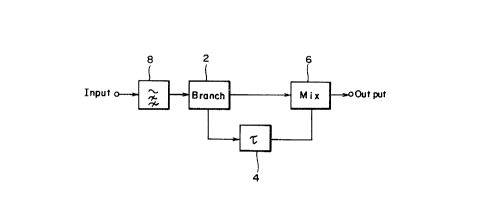
FIG. 7 is a block diagram showing a third
embodiment of the frequency discriminator of the present
invention. In the present embodiment, there is provided
a bandpass filter 12 having a cutoff frequency on the
high frequency side fH and a cutoff frequency on the low
frequency side fL in place of high-pass filter 8 in the
first embodiment of FIG. 3. Accordingly, the
arrangement of the present embodiment has both the
characteristics of the first embodiment of FIG. 3 and
the second embodiment of FIG. 5.
FIG. 8A, FIG. 8B, and FIG. 8C correspond to
FIG. 4A, FIG. 4B, and FIG. 4C, respectively. When the
~7~?~
center frequency fI F of the intermediate-frequency
signal and delay time ~ are set up to satisfy the
expression (2), the cutoff frequency on the high
frequency side fH and cutoff frequency on the low
frequency side fL are set up such that
fH = (2n + 3)/4~ (5)
fL = (2n - 1)/4r .,. (6)
respectively. When, for example, n is set such that n =
2 and AFC is performed such that the center frequency
0 fI F of the intermediate-frequency signal is stabilized
at the point B, fH and fL become such that fH = 7/4~ , fL
= 3/4 r .
In this case, as shown in FIG. 8C, while the
lower limit of the capture range is -5/4~ , the upper
limit of the capture range disappears theoretically and,
hence, the capture range is greatly widen. Further, the
accuracy in frequency identification becomes higher at
the point B.
Functioning of the third embodiment of FIG. 7
was actually verified using a bandpass filter of a
Tchebyshev type. The cutoff frequency on the low
frequency side fL of the bandpass filter was 3GHz and
the cutoff frequency on the high frequency side fH was
7GHz. The delay time ~ in the delay circuit 4 was set
~7~
to 250psec.
First, actually measured data of
characteristics when sine waves, not modulated
intermediate-frequency signals, were input are shown in
FIG. 9A, FIG. 9B, and FIG. 9C. FIG. 9A shows the
frequency discrimination characteristic when the
bandpass filter was not used (corresponding to the prior
art) and this corresponds to FIG. 8A. FIG. 9B shows the
frequency characteristic of the bandpass filter and this
corresponds to FIG. 8B. FIG. 9C shows the frequency
discrimination characteristic in the arrangement with
the bandpass filter inserted and this corresponds to
FIG. 8C. That the output voltage of the frequency
discriminator takes on small positive values in the
frequency region higher than the cutoff frequency on the
high frequency side fH in the frequency discrimination
characteristic of FIG. 9C is considered due to the fact
that the cutoff characteristic of the bandpass filter
used was broad.
Actually measured data of frequency
discrimination characteristic obtained when a modulated
intermediate-frequency signal obtained by heterodyne
detection was input to this frequency discriminator is
shown in FIG. 10. The intermediate-frequency signal was
t~
-
~ ~ 7 1 ~ 2 ~
obtained through heterodyne detection by having a signal
light beam emitted from a laser diode, which is
frequency modulated, phase modulated, or amplitude
modulated, mixed with a local light beam from another
laser diode. The bit rate in the modulated signal was
2.5Gbit/sec and the center frequency of the
intermediate-frequency signal was 5GHz. According to
the results of the experiment, although the output
voltage of the frequency discriminator is taking on
positive values in the frequency region higher than the
cutoff frequency on the high frequency side f~ due to
unexcellent cutoff characteristic of the bandpass
filter, it is apparent that the capture range is
expanded on the low frequency side.
In the above described embodiments, even when
the center frequency of the intermediate-frequency
signal is greatly apart from the passband of the filter
(high-pass filter 8, low-pass filter 10, or bandpass
filter 12), AFC can be performed theoretically
provided that the center frequency is present within the
capture range. However, when the integration of power
of the high-order spectrum of the intermediate-frequency
signal within the passband of the filter is small, it is
possible that the polarity of the output voltage of the
~@71~ ~,J~
frequency discriminator is erroneously detected and the
normal AFC operation is impaired. In order to eliminate
such possibility, an embodiment as shown in FIG. 11 or
FIG. 12 is proposed. In FIG. 11, there is provided a
limiter 20 or a gain saturation amplifier 22 between the
high-pass filter 8, low-pass filter 10, or bandpass
filter 12 and the branch circuit 2. In the limiter 20,
the output amplitude is limited for the input amplitude
larger than a predetermined value, and in the gain
saturation amplifier 22, the output power is limited for
the input power larger than a predetermined value. By
such embodiment, even when the center frequency of the
intermediate-frequency signal is apart from the passband
of the filter, the power of the harmonic components of
the intermediate-frequency signal is compensated for so
that the erroneous detection of the polarity of the
output voltage of the frequency discriminator is
prevented. Consequently, an effective expansion of the
capture range can be attained.
An automatic gain control (AGC) circuit 24 may
be provided, instead of the limiter or gain saturation
amplifier, between the high-pass filter 8, low-pass
filter 10, or bandpass filter 12 and the branch circuit
2 as shown in FIG. 12. The gain in the AGC circuit 24
-
~ 7~ ~-i 2~
is controlled such that the power of the signal input to
the branch circuit 2 becomes constant. Also by this
embodiment, an effective expansion of the capture range
can be attained.
While, in the embodiment shown in FIG. 11 or
FIG. 12, there is provided only one of the limiter 20,
gain saturation amplifier 22, and AGC circuit 24, a
combination of two or three of them connected in series
may be used, instead.
FIG. 13 is a graph for comparison of actually
measured data of frequency discrimination
characteristics between the cases with the AGC circuit
provided and not provided. The solid line indicates the
frequency discrimination characteristic in the case
where the AGC circuit is provided and the broken line
indicates the frequency discrimination characteristic in
the case where the AGC circuit is not provided. It is
apparent from the graph that the positive output of the
frequency discriminator is increased in the region
around the point where the intermediate frequency
becomes zero by the compensation for the harmonic
components in the intermediate-frequency signal made by
the AGC circuit.
FIG. 14 is a block diagram of a heterodyne
~1 '
2~7~ ~2~
receiver for coherent lightwave communications to which
the frequency discriminator of the present invention is
applied. A signal light beam including modulated
components transmitted over an optical transmission line
is input to an optical coupler 28 together with a local
light beam from a local light source 26. In the optical
coupler 28, the signal light beam is mixed with the
local light beam and the mixed light beam is subjected
to heterodyne detection in an optical detection circuit
30 including a photodiode and the like. As a result of
the heterodyne detection, an intermediate-frequency
signal is output from the optical detection circuit 30.
The intermediate-frequency signal is turned into a
baseband signal in a demodulator 32. The intermediate-
1~ frequency signal from the optical detection circuit 30is also input to the frequency discriminator 34
according to the present invention. The frequency
discriminator 34 is arranged for example as shown in
FIG. 12. An automatic frequency control (AFC) circuit
36 controls the frequency of the local light beam such
that the output voltage of the frequency discriminator
34 becomes a constant value (for example zero). The
frequency of the local light beam, when the local light
source 26 comprises a laser diode, can be varied for
~ @ ~
example by adjusting the bias current for the laser
diode.
When AFC is performed by applying the
frequency discriminator of the present invention to a
heterodyne receiver for coherent lightwave
communications as described above, the stability of the
center frequency of the intermediate-frequency signal is
improved and, because of the expanded capture range, the
frequency range over which AFC is achieved can be
expanded.
As described in the foregoing, the provision
of a frequency discriminator which has high accuracy in
frequency identification and a wide capture range can be
attained.
While the invention has been described with
reference to particular embodiments, these embodiments
are given by way of illustration only and not limitative
of the present invention. The scope of the invention is
defined by the appended claims and all changes and
modifications as fall within the equivalence of the
scope of the claims are therefore to be embraced by the
invention.