Note: Descriptions are shown in the official language in which they were submitted.
207~
ELECTRONICALLY RECONFIGURABLE ANTENNA
Fiel~ of_the Invention
This invention relates to multiple element
anten~a arrays capable of operation in plural wave
propagation modes, and more particularly relates to
electr~nically reconfigurabla array antennas comprising
a plurality of active and parasitic antenna elements.
ack~rQund oP the Invention
A number of prior patents disclose antennas
capable o operation to provide varying electroma~netic
wave propagation.
U.S. Patent No. 3,560,978 discloses an
~lectronically controlled antenna system comprising a
monopole radiator surrounded by two or more concentric
circular arrays of parasitic elements which ar~
electively operated by digitally controlled ~witch:ing
diodes. In the antenna system of U.S. Patent No.
3,560,978, recirculating shi~t registers are used to
inhibit the parasitic elements in the circular arrays
to produce the desired rotating wave pattern.
U.S. Patent No. 3,877,047 relates to an
electronically scanned, multiple element antenna array
in combinatiQn wi~h means for chansing its operation
between a multiple element array and an end-fire mode
o~ operationO In the antenna of U.S. Patent
No. 3,877,014, a transmitter is switched to feed either
a cQlumn array of antenna elements or the end-fire feed
element. During end-fir~ operation, the column array
of antenna elements are short circuited.
U.S. Patent No. 3,883,~75 discloses a linear array
antenna adopted for commutation in a simulated Doppler
ground beacon guidance system. In the end-fire
co~mutated antenna array o~ U.S. Patent No. 3,883,875,
th~ linear array of n radiator elements is combined
with a transmitting means for exciting each of the n-1
--1--
2 ~ 7 ~ '~
of said elements in turn, and an electronic or
mechan~cal commutator providing for successive
excitation in accordance with the predetermined
progra~. Means are provided for short circuiting and
open circuiting each of the n-1 elements, and the short
circuiting and open circuiting means is operated in
such a manner that during excitation of any one of said
elements, the element adjacent to the rear of the
excited elements operates as a re~lector and the
remaining n-2 elements remain open circuited and
therefore electrically transparent. A permanently
non-excited element is located at one end of the array.
In "Reactively Controlled Directive Arrays'7, IEEE
Transactions on Antennas and ProPa~ation, Vol. ~-26,
No. 3, May, ~978, Roger F. Harrington discloses that
the radiation characteristics of an n-port antenna
syst~m can he controlled by impedance loading the ports
and ~eeding only one or several of the ports. In
Harrington's disclosed system, reactive loads can be
used to resonate a real port current to give a
radiation pattern of high directivity. As examples of
the system, Harrington discloses a circular array
antenna with six reactively loaded dipoles equally
spaced on a circle about a central dipole which is fed,
and a linear array of dipoles with all dipoles
reactively loaded and one or more dipoles excited by a
source. In operating the circular array antenna,
Harrington discloses that by varying the reactive loads
of the dipoles in the circular array, it is possible to
change the direction of maximum gain of the antenna
array about the central fed element and indicates that
such reactively controlled antenna arrays should prove
useful for directive arrays of restricted spatial
extent.
U.S. Patent No~ 4,631,546 discloses an antenna
which has a transmission and reception pattern that can
electrically altered to provide directional signal
2~7~
pa~terns that can be electronically rotated. Th~
antenna of U.S. Patent No. ~,631,546 is disclosed as
having a central driven antenna element and a plurality
o~ surrounding parasitic elements combined with
circuitry for modifying the basic omni-directional
pattern of such an antenna arrangement to a directional
pattern by normally capacitively coupling the parasitic
elem~nts to ground, but on a selective basis, changing
some of the parasitic elements to be inductively
coupled to ground so they act as refl~ctors and provide
an eccentric signal radiation pattern. By cyclically
altering the connection of various parasitic elements
in their coupling to ground, a rotating directional
signal is produced.
U.S0 Patent No. 4,700,197 discloses a small
linearly polarized adaptive array antenna for
communication systems. The antenna of U.S. Patent
No. 4,700,197 consists of a ground plane formed by an
electrical conductive plate and a driven quarter wave
monopole positioned centrally within and substantially
perpendicular to the ground plane. The antenna further
includes a plurality of coaxial parasitic elements,
each oE which i5 positioned substantially perpendicular
to but electrically isolated from the ground plane and
arranged in a plurality of concentric circles
surrounding the central driven monopole. The
surrounding coaxial parasitic elements are conneeted to
the ground plane by pin diodes or other switching means
and are selectively connectable to the ground plane to
alter the directivity of the antenna beam, both in ~he
azimuth and elevation planes.
Patent No. 3,109,175 discloses an antenna systeTn
to provide a rotating unidirectional electromagnetic
wave. In the antenna system o~ U.S. Patent No.
3,109,175, an active antenna element is mounted on a
stationary ground plane and a plurality of parasitic
antenna elements are spacPd along a plurality o~ radii
-3-
~7~
extending outwardly from the central active antennaelement to provide a plurality of radially extending
directive arrays. A pair of parasitic elements are
mounted on a rotating ring, which is located between
the central active antenna element and the radially
extending active arrays o~ parasitic elements and
rotated to providP an antenna system with a plurality
of high gain radially extending lobes.
In addition, U.S. Patent Nos. 3,096,520,
3,218,645, and 3,508,274 disclose antenna systems
comprising end-fire arrays.
Antenna systems including multiple active antenna
elements with phasing electronics and/or phased
transmitters are disclosed, for example, in U.S. Patent
No~. 3,255,450, 3,307,188, 3,495,263, 3,611,401,
4,090,203, 4,360,813 and 4,849,763.
Antennas comprising a plurality of antenna
elements in a planar array are also known. For
example,0
U.S. Patent No. 4,797,682 discloses a phased array
antenna structure including a plurality of radiating
elements arranged in concentric rings. In the antenna
of U.S. Patent No. 4,797,682, the radiating elements of
each concentric ring are of the same size, but the
radiating elements of different rings are different
sizes. By varying the size o~ the radiating elements,
the position of the elements will not be periodic and
the spacing between adjacent rings will not be equal.
Thus, grating lobes are minimized so they cannot
accumulate in a periodic manner.
Notwithstanding this extensive developmental
effort, problems still exist with multiple element
antenna arrays, particularly with the performance of
large apertures steered to end fire.
For a beam to be formed across the upper surface
oP an antenna array such as that show~ in U.S. Patent
No. 4,797,682, each radiating element rnust be cap~ble
of delivering power across the face of the array,
--4--
207:17~
ultimately radiating along the ground plane and into
free space at the horizonO In large antenna arrays
consi~ting of plurality of antenna elements and having
diameters in excess of 10 wavelengths, the elements
will receive much of this power, and act like a very
105sy surface. In short, such large arrays tend to
re-absorb a large portion of the power that is intended
to be radiated. This effect is well known, and is
often described in terms of mutual coupling effect~, or
activ~ array reflection coefficient.
The plot in Fig. 1 describes one of the results of
a 1983 Lincoln Labs study of phased arrays with wire
monopole radiating elements. Gain-referenced patterns
are plotted for a single central element embedded in
many si~es of square arrays on an infinite ground
plane. Fi~. 1 indicates that the horizon gain of a
single element falls drastically as the size of the
array increases. For a 15-wavelength antenna, an
element gain degradation of some 15.0 dB would be
expec~ed.
Similar results are obtained when comparing an
isolated low-profile monopole, and the same element
embedded in a 15 wavelength 1306-element circular array
of identical low-profile monopoles. In this case, such
antennas were mounted on a ground plane approximately
40 wavel~ngths in diameter. The maximum measured gain
of th~ isolated element was approximately 5.15 dBil at
10 above the horizon. When embedded in the center of
the 1306-element array, the element had measured gain
of -11.1 dBil at 10 above the horizon, corresponding
to 16.25 dB degradation.
Because not all elements are effected as severely
as the one~ measurad in the center of such an array, it
ls difficult to make an array gain estimate.
Furthermore~ some degree of active matching is
possible, which should marginally improve the gain.
Even so, the end-fire gain of this large circular array
lL 7 ~1 ~
will almost certainly not exceed 1~.0 dBil, and may be
as low as 13.0 dBil. Such gain is too low for the
investment in apertures, and an intolerable thermal
proble~ will result fro~ more than 12.0 dB of RF power
dissipation in the transmit mode.
Statement of ~he Invention
This invention provides an electronically
reconfigurable antenna in which individual antenna
element~ can be reconfigured as active or parasitic
ele~ents in the procass of variable mode operation. In
antenna of this invention, a~ acti~e subset of antenna
elements excites a wave on a parasitic subset of
antenna elements, which are controlled by
electr~nically variable reactances to provide a
non-complex and reliable, compact and li~htweight,
relatively inexpensive and efficient antenna system
capable o~ operation in a plurality of modes of wave
propagation.
In the invention, a plurality of electronically
variable reactances is used to provide a reconfigurable
array, which may operate in a plurality of modes of
wave propagation. Furthermor2, the plurality of
variable reactances allow compensation for the
inherently narrow operating bandwidth of the high-gain
sur~ace wave antennas.
This invention provides an electronically
reconfigurable antenna including a plurality of antenna
elements supported in an array adjacent and
dielectrically isolated from a ground plane and adapted
so that one or more of said antenna elements comprises
active antenna elements driven from a source of
electromagnetic energy and a plurality of the remainder
of said antenna elements comprise antenna elements
parasitically coupled to the one or more active antenna
element~ in said array. In the invention, a plurality
of the remainder of said parasitic antenna elements are
20P7:L7~
electrically connected to the adjacent ground plane by
electronically varia~le reactances, which provide first
reactances between the plurality of the remainder of
the parasitic antenna elements to provide a first wave
propagation characteristic of the antenna and second
reactances between the plurality o~ the remaind~r of
said parasitic antenna elements to provide a second
wave propagation characteristic of the antenna.
In the invention, the plurality of antenna
elements can form a linear, planar or curved surface
array with the first reactances providing a first wave
propagation characteristic and the second reactances
providing a second wave propagation characteristic; the
electronically variable reactances can comprise MMIC
chips; and the plurality of active antenna elements can
be driven from the source of electromagnetic energy
through a plurality of phase shifters.
Other features and advantages of the invention
will be apparent from the drawings and detailed
description of he invention which follows.
Brief Description of t _ Drawlnqs
Fig. 1 is a graphical prior art comparison of
phased arrays demonstrating the gain degradation of a
single element as the size of the array increases;
Fig. 2 is a diagrammatic illustration of the
invention;
Fig. 3 is a diagram showing the manner of
switching elements of antennas of the invsntion from
active to parasitic modes of operation;
Fig. 4 is a diagrammatic plan view of a circular
array antenna of the invention adapted to provide a
plurality of active bands of elements to provide
steerable horizontal wave propagation;
Figs. 5 and 6 are diagrammatic illustrations of an
antenna element feed system for an antenna, such as the
antenna of Fiq. 4, showing one manner in which
2 ~ 7 ~
electromagnetic energy can be distributed between and
collected from the active antenna elements;
Figs. 7 and 8 are diagrammatic plan views of a
preferred circular phased array antenna using this
invention;
Fig~ 9 is a measured radiation pattern of a
circular phased array antenna of the invention with 64
active elemants elements, demonstrating an azimuthal
conical pattern at 10 elevation;
Fig. 10 is a measured radiation pattern of another
circular phased array antenna of th~ invention with 128
active elements, demonstrating an azimuthal conical
pattern at 10 elevation;
Fig. 11 is a measured radiation pattern of the
circular phased array o~ Fig. 9, with 64 active
elements/ demonstrating an Plevation pattern; and
Fig. 12 is a measured radiation pattern of a
circular phased array of Fi~. 10, with 128 active
elements, demonstrating an elevation pattern.
Best Mode o~ the Invention
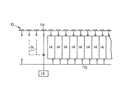
Fig. 2 is a diagrammatic illustration of an
electronically reconfigurable antenna 10 of the
invention. As shown in Fig. 2, a plurality o~ antenna
elements 11 are supported in an array adjacent and
dielectrically isolated from a ground plane 12. At
least one of the antenna elements lla comprises an
active antenna element driven from a source of
electromagnetic energy 13. A plurality of the
remainder of the antenna elements llb comprise antenna
elements parasitically coupled to the at least one
active antenna element lla in said array. The
plurality of antenna elements llb of the remainder of
antenna elements 11 are electrically connected to the
adjacent ground plane 12 by electronically variable
reactances 14. The electronically variable reactances
14 provide first reactances between ground and the
antenna elements llb of the plurality of the remainder
of antenna elements to provide a first wave propagation
characteri~tic of the antenna 10 and second reactances
between ground and the antenna elements llb o~ the
plurality of the remainder of antenna elements to
provide a second wave propagation characteristic of the
antenna.
The f irst xeactances of the electronically
varia~le reactances 14 can be selected to provide a
surface wave propagation characteristic and the second
reactances can be selected to provide a lea~y wave
propagation characteristic.
As indicated in Fig. 2, in its simplest form, the
plurality of antenna elements 11 can ~e supported in a
linear array. Also, as indicated by phantom lines :llc
in Fig. 2, a plurality of antenna elements can comprise
active antenna elements driven ~rom the source of
electromagnetic energy 13. Xn addition, the plural:ity
of active antenna elements can be driven from the
source of electromagnetic energy 13 through a plurality
of phase ~hifters.
In preferred embodiments of the invention, each
antenna ~lement 11 can be connected to an MMIC chip or
hybrid device 15 which, as shown in Fig. 3, can include
the electronically variable reactance 14, and also an
amplifier 16 and phase shifter 17, and electronically
controlled switching element 18 to connect the antenna
eleme~t to the ground plane 12 through electronically
variabl~ reactance 14 when the antenna element is to
operate as a parasitic element and to connect the
antenna element 11 through the amplifier 16 and phase
shifter 17 to the source of electromagnetic energy 13
when the antenna element is to operate as an active
antenna element. The electrical connections to operate
the components of the MMIC chip 15 have been omit~ed
from the drawings for clarity, but may be provided by
appropriate electrical conductors, as known in the art.
2~71~
Fig. 4 shows an embodiment 20 of the invention in
which a plurality of antenna elements 21 are formed in
a cir¢ular array on a substantially planar dielectric
surface. The circular planar array of antenna ele~ents
21 may be formed from conductor-clad printed circuit
board by etching away the conductor, as well known in
the microstrip antenna art. In the antenna of the
invention, the plurality of antenna elements ~1 are
connected, as described herein, to provide one or more
active ~ubsets of antenna elements and associated
parasitic subsets of antenna elements. The antenna
elements 21 of the circular array 20 may be provided
with electronically variable reactances, as described
above.
In the embodiment of the invention shown in Fis3.
4, the circular array of antenna elements may provide
operatlon much like a plurality of parallel Yagi-Uda
arrays. The number of antenna elements is sufficient
to ~orm a plurality of active subsets of active antenna
elsments and associated subsets of parasitic antenna
elements. Each of the plurality of active subsets form
a band of active antenna elements like BAND A,
containing active antenna elements 2la, and BAND B
containing active antenna 21ements 2lb. As shown in
Fig. 4, ~AND A and BAND B extend in different
dire~tions in the circular array.
For a given azimuth scan angle, a subset of the.
elements 21a in BAND A or 21b in BAND B, is selectecl as
tha active subset, analogous to the single element and
re~lector excitation of the Yagis. A large number of
active elements may be used to distribute high transmit
p~wer, and so their excitation can be phased to
optimize the launch efficiency of the surface wave. To
maximize broadside launch directivity, each band of
active elements (i.e., BAND A with elemen~s 21a, BAND B
with elements 21b...or BAND n with elements 21n) should
have an extent equal to the array diameter. The
--10--
2 0 ~
antenna elements in front of an active subset in the
direction of wave propagation, such as antenna elements
21c in front of BAND B, will be parasitic, loaded with
a distribution of reactances that will maximize gain
and control sidelobes in the pattern. Antenna elements
to the rear of the active band, such as antenna
elements 21d to the rear of BAND A, may be loaded to
suppress bacXlobes. The antenna elements 21¢ and 2ld
are parasitic antenna elements forming a parasitic
subset of parasitic ant~nna elements associated with
the BAND B active antenna elements. As is readily
apparent, associated parasitic subsets of antenna
elements may be formed to the front and rear o~ the
active antenna elements 21a of the BAN~ A subset.
To change the azimuth steering angle, a different
active band ~compare BAND A and BAND B of Fig. 4) is
chosen, as well as a different distribution of
para~itic reactances. Fig. 3 illustrates the circuit
elements connected to the antenna elements to switch
them between their active and passive roles. The
variable reactance will have the same complexity as a
5-bit phase shifter with only one port. In antennas of
the invention every element can be versatile, having a
full T/R module along with the switching and variable
reactance capability to become parasitic, but in many
effective antennas of the invention, it is not
necessary that every element have such capability and
versatility.
Figs, 5 and 6 show, as well known in the art, how
electromagnetic energy may be distributed and collected
from the antenna elements. The antenna elements 21 can
~e organized in pairs, and connected with a compact
two-way power divider/combiner 31 (Fig. 6), each with
its own output connector. The phasing between the two
antenna elements of each power combiner can follow
normal geometric techniques for end-fire steering. In
order to arrive at the correct phasing relationships
--11--
2~71rl ~ ~
for the rest of the antenna element feed system, the
~ar field phase at 10 elevation can be measured for
all of the two-element arrays. This phase data can
then be used for all phasing relationships in upper
levels o~ the antenna element feed system.
The connector ports for the plurality of two-way
power diYiderlcombiners can be organized into groups vf
8, then conne~ted to 8-way power combiners with
phase-compensated cables. Fig. 5 shows a schematic
bac~ view of an 128-way feed syste~ 30, which includes
16 8-way power combiners 32, further combined by 2
8-way collectors 33 and finally by a 2 way combiner 34
at the input. Section 6-6 of Fig. 5 i5 shown in Fig.
6, with the connection of 8 2-element combiners 31 to
one of the 16 8-way power combiners 32.
Any required phasing can be providsd by varying
the lengths of cables 36 to provide the measured phase
di~erences. For the first level of 8-way power
combiner, these differences can be small because the
antenna elements 21 can be almost in a line orthogonal
to the steering direction. The major phasing can be
accomplished by the cables between the 8-way power
combiners 32 and the 8-way collector boards 33, or by
separate phase shifters.
As shown and described above, the invention
pro~ides an electronically reconfigurable ant~nna with
an array of antenna elements having an extent of
several wavelengths over an area, such as a circle,
rectangle or other area useful in phased microwave
arrays. The antenna elements ~11, 21) of the array are
sufficient in number to permit the formation of a
subset of active antenna elements adapted to provide
desired wave propagation characteristics such as beam
width and direction, and to permit a subset of
para~itic antenna elements adapted to assist the subset
of active antenna elements in achieving desired wave
propagation characteristics. The antennas can includP
-12-
7 ~ ~
an antenna element feed system providing a connection
to each antenna element that can be electrically
switched between an electronically variable reactance
and a source and/or receiver of electromagnetic energyO
The feed system can be controllable to provide
connections between a plurality of antenna elements and
the source/receiver of electromaynstic energy to form
an active subset of antenna elements to provide the
desired wave propagation characteristics of the
antenna. The feed system can also be controllable to
provide connections between a plurality of the
remainder of the antenna elements and their associated
electronically variable reactances in a subset of
parasitic antenna elements that provide substantially
lossless assistance in achieving the desired wave
propagation characteristics of the antennaO
The invention can be used to provide antennas with
a feed system that can be controlled to provide
electronic scanning oP the horizon, and surface wave
enhancement. The feed system can also be controlled to
vary th~ alectronically variable reactances andlor the
number and locations of the parasitic antenna elements
in the parasitic subset of antenna elements to provide
from the antenna both surface wave and leaXy wave
propagation for elevation scanning. Furthermore, the
electronically variable reactances can allow
compensation for the narrow operating bandwidth of such
high gain antennas and proYide an antenna capable of
operating over a broader bandwidth than formerly
possible.
An antenna as shown in Fiys. 7 and 8 may provide a
preferable mode of the invention and better results
with an active band of lesser extent than the antenna
shown in Fig. 4. The antenna surface is like the
antenna surface of the antenna o~ Fig. 4, and .it is
supported adjacent a ground plane with an antenna
element feed system including components like those
-13-
2 ~
described above, but connected and operated differentlyand more simply, as set forth below. As illustrated in
Fig. 7, the antenna elements of only one or two outer
rings 42, ~3 (or at most, about 256 elements) need ever
be active elements. The rest of the array (or about
1,050 antenna elements~ can include only the
electronically vari~ble reactance, which can be a MMIC
chip with very low weight and power requirement. Nor
is it required that the parasitic surface be made up of
the same antenna elements as the active elements, as
long as the reactive surface formed by the subset of
parasitic antenna elements can be varied
electronically.
In the antenna 40 of Figs. 7 and ~, the antenna
ele~ents included in the active subsets are selected in
different sec~ors ~44, 45...) o~ the two or more
concentric rings 42, 43. As shown in Fig. 8, surfac:e
wave excitation may be enhanced by switchable reflector
elements ~46a in BAND Al 46b in BAND B) on the
outermost concentric ring 46 of the array. The
remainder of the elements of the array, as before, ar~
loaded with a distribution of reactances to ac~ieve the
desired surface wave parameters. ~canning, or steering
o~ the propagated wave is again accomplished by
changing the position of active elements that make up
the active subset sectors (44,45...) by locating them
on different diameters (~7,48...) aligned with the
direction of beam steering (compare BAND A and BAND B).
The parasitic element distribution may also be changed.
In this embodiment o~ the invention, the antenna
elements of at least one of the outer concentric rings
42, 43 are adapted to be connected to a source of
electromagnetic ener~y to provide one or more active
antenna elements within a plurality of active subsets
within different sectors, e.g., BAND A, BAND B, of at
least one outer concentric ring 42, 43. A plurality of
dif~erent sectors of active antenna elements are
-14-
2~ 71~
located about the outer concentric ring or rings 42, 43
on a plurality of diameters (e.g., 47, 48). The
remaining antenna elements 41 of other concentric rings
at least on or adjacent said plurality o~ diameters
(e.g., 47, 48~ are electrically connected to th~
ad~acent ground plane by electronically variable
reactances to provide selectably parasitic antenna
elements on or adjacent the plurality of diameters.
The active antenna elements and the parasitic antenna
elements on or adjacent said plurality of diameters can
provide surface wave propagation characteristics with
first reactances of the electronically variable
reactances and leaky wave propagation characteristics
with second reactances of the electronically variable
reactances and the plurality of antenna elements o~ the
array can be controlled to electronically scan around
the plane of the array, and, for example, the horizon.
In preferred embodiments, at least one oP said outer
concentric rings 42, 43 of selectively active elements
lies wi~hin the outermost concentric ring 46 of antenna
elements, and the outermost of the outer concentric
rings 46 is electrically connected to the adjacent
ground plane by electronically variable reactances
providing first and second reactances to reflect the
electromagnetic wave propagated by the subset of active
element~, e.g., BAND A and BAND B.
The antenna of Figs. 7 and 8 may represent huge
savings in weight, power requirement, complexity,
reliability and cost, compared to the antenna of Fig.
4.
It is believed that the horizon gain oP a 15
wavelengths circular phased array of this invention may
be as hiqh as 26 dBil.
Measurements were made with a fixed-beam antenna
of the invention, built in the form of Fig. 4 with
centerbands of 64 and 12~ active elements, mounted on a
7.5' ground plane, which results in the peak of an
2~:L7~
end-fire beam occurring at approximately 10 elevation.
Both elevation and az.imuthal conical cuts were taken,
with the conical cuts taken through the peak of the
elevation beam at 10. Figs. 9 and 10 present conical
patterns for ~-element and 128-element active arrays
of the invention at 4.~ GHzo
Fig. 9 is the 10 conical for the 64-element
active band. As shown in Fig. 9, the beam is very well
formed with sidelobes only slightly his~her than would
be expected for the uniform amplitude clistxibution
used. The measured peak gain was 21.07 dBil, and the
antenna suffered a loss of about 2.35 dB in the feed
system. The aperture gain for this pattern was
therefore about 23.45 dBil. Similarly, Fig. 10 is
the 10~ conical for the 128-element active band. In
this case, the peak gain was 20.77 dBil with 2.65 dB
loss in the feed system, yielding coincidentally the
same aperture gain of 23.45 dBil. These aperture gains
correspond favorably to ideal array values of about
26dBil, if element efficiencies, element mismatches and
mutual coupling losses are taken into account.
Figs. 11 and 12 are the elevation patterns for the
antennas with 64 elements and 128 elements,
respectively. Both elevation patterns (Figs. 11 and
12) ha~e extremely high sidelobe levels, which
represents the direct radiation (i.e., no~ coupled to
the surface wave) of the active band arrays. The
elevation beam of the 128-element antenna (Fig. 12) is
considerably narrower than the elevation beam of the
64-element antenna (Fig. ~1). This effect is easily
~xplained by the higher directivity, and resulting
surface wave launch ef~iciency, of 4 rows steered to
end-fire (128-element active band) as opposed to 2 rows
(64-element active band). The fact that the net
aperture gain was almost the same in the two cases is a
result of higher mutual coupling losses in the
128-element case, since the directivity must be higher.
2~ 7~
The tahle I (below) summarizes the gain re~ults at
4~8 GHz. A rough measurement of directivity was also
made, in order to estimate the aperture efficiency,
which would include element efficiency, element
mismatch loss and mutual coupling loss. This
mea~urement is the result of taking amplit~de
measurements over ~ll space and perforrning the
appropriate weighted summations. Some error is to be
expected due to granularity in summing over the very
narrow azimuth beam, and the directivity values
obtained seem high compar~d to theoretical estimates iYI
light of what appears to be non-optimum launch
ef~iciency.
TABLE I
64 ELEMENTS 128 ELEMENTS
ACTIVE ACTIVE
GAIN 21.1 dBil 20.8 dBil
FEED LOSS 2.35 dB 2.65 dB
APERTURE GAIN23.45 dBil 23.45 dBil
DIRECTIVITY26.4 dBil 27~1 dBil
APERTURE 3.0 dB 3.7 dB
EFFICIENCY
As shown above, the invention can provide an
electronically reconfigurable antenna capable of plural
wave propagation and a steerable high gain beam at very
low angles to a planar aperture.
While certain and presently known preferred
embodiments of the invention are illustrated and
described above, it will be apparent to those skilled
in the art that the invention may be incorporated into
other embodiments and antenna systems within the scope
of the invention as determined from the following
claims.
-17-