Note: Descriptions are shown in the official language in which they were submitted.
~ ~ 7 ~ ~ 6g
~ .- A CARRIER RECOVERY METHOD AND APPARATUS
HAVING AN ADJUSTABLE RESPONSE TIME
DETERMINED BY CARRIER SIGNAL PARAMETERS.
Field of the Invention
The present invention relates generally to
10 communication receivers, and, more particularly, to a
communication receiver with a carrier recovery method
and apparatus having an adjustable response time
determined by carrier signal parameters. Reference is
made to U.S. Patent No. 5,083,304, filed on behalf of
Stephen Vincent Cahill on the same date herewith,
containing related subject matter, and assigned to the
assignee of the present invention.
Background of the Invention
A radio communication system is comprised, at
minimum, of a transmitter and a receiver. The
transmitter and the receiver are interconnected by a
radio-frequency channel to permit transmission of an
information signal therebetween.
Typically, the information signal is impressed upon
a radio-frequency electromagnetic wave by a process
30 referred to as modulation to permit transmission of the
information signal between the transmitter and the
receiver. The radio-frequency electromagnetic wave is
referred to as a carrier wave which is of a particular
frequency, and the carrier wave, once modulated by the
2071869
information signal, is referred to as a modulated
information signal. The modulated information signal
may be transmitted through free space to transmit
thereby the information between the transmitter and the
receiver.
Various modulation techniques have been developed
to modulate the information signal upon the
electromagnetic wave. Amplitude modulation (AM),
frequency modulation tFM), phase modulation (PM), and
composite modulation (CM) are four of such modulation
techniques. Frequency and phase modulation techniques
are collectively known as angle modulation.
In general, an amplitude modulated signal is
formed by impressing (i.e., modulating) an information
signal upon a carrier wave such that the information
signal modifies the amplitude of the carrier wave
corresponding to the value of the information signal.
An angle modulated signal formed is formed by
impressing (i.e., modulating) an information signal upon
a carrier wave such that the information signal modifies
the phase (or the time differential of phase, frequency)
of the carrier wave corresponding to the value of the
information signal. Angle modulation does not cause the
amplitude of the carrier wave to vary, and the
information content of the modulated information signal
is contained in the variation of the phase (or frequency)
of the signal. Because the amplitude of an angle
modulated signal does not vary, an angle modulated
signal is referred to as a constant envelope signal.
A composite modulated signal is formed by
impressing (i.e., modulating) an information signal upon
a carrier wave such that the information signal modifies
both the amplitude and the phase of the carrier wave.
Conventionally, in order to form the composite
2071869
modulated signal, the carrier wave (or a carrier
intermediate frequency, i.e., IF, source) is first
separated into sine wave and cosine wave carrier
portions. Separate portions, referred to as the in-phase
(or 1) and the quadrature (or Q) components, of the
information signal are impressed upon the cosine wave
and sine wave carrier portions of the carrier wave,
respectively. The sine wave and cosine wave
components are then recombined, and the resultant
signal, the composite modulated signal, varies in both
amplitude, and, additionally, phase. Composite
modulation is advantageous in that a composite
modulated signal permits a greater amount of
information to be transmitted within a frequency
bandwidth than a signal generated by any of the
previously mentioned modulation techniques. See, for
instance, a discussion in the text Introduction to
Communication Systems, 2nd Ed, by Ferrel G. Stremmler,
ISBN 0-201-07251-3, pages 590-596.
A family type of composite modulation is
quadrature amplitude modulation (QAM). In this
modulation method, as conventionally applied to a binary
information source, the binary data stream is separated
into bit pairs. The individual bits of the bit pairs are
converted from unipolar to bipolar format, passed
through a pair of electric wave filters, and applied to
the multiplier pair whose other inputs are the sine and
cosine components of the carrier or carrier IF signal. A
particular type of QAM is 7~/4-shift DQPSK (for
differential quadrature phase shift keying), in which the
input data stream is encoded so that the composite
modulated carrier shifts in increments of +J~/4 or +3~/4
according to the input bit pairs. This modulation
method, conventionally implemented, is discussed in
2071869
Digital Communications, by John G. Proakis, 1st Ed., ISBN
0-07-050927-1, pages 171-178.
A receiver which receives a modulated information
signal, such as a one formed by one of the above
5 described modulation techniques, includes circuitry to
detect, or otherwise to recreate, the information signal
modulated upon the carrier wave. This process is
referred to as demodulation. As many different
modulated information signals may be simultaneously
10 transmitted by a plurality of transmitters at a plurality
of different frequencies, a receiver contains tuning
circuitry to demodulate only those signals received by
the receiver which are of certain desired frequencies.
The broad range of frequencies at which modulated
15 information signals may be transmitted is referred to as
the electromagnetic frequency spectrum. Regulation of
radio-frequency communications in certain frequency
bands of the electromagnetic frequency spectrum
minimizes interference between simultaneously
20 transmitted signals.
For example, portions of a 100 MHz band of the
electromagnetic frequency spectrum (extending between
800 MHz and 900 MHz) are allocated for radiotelephone
communication, such as, for example, communication
25 effectuated by radiotelephones utilized in a cellular,
communication system. Existing radiotelephones contain
circuitry both to generate and to receive radio-frequency
modulated information signals.
A cellular communications system is created by
30 positioning numerous base stations at specific locations
throughout a geographical area. Each of the base
stations is constructed to receive and to transmit
modulated information signals simultaneously to and
from radiotelephones to permit two-way communication
2071869
there between. Each of the base stations is provided
with means to communicate with one or more switching
offices which permit connection to the conventional
telephone network.
The base stations are positioned at locations such
that a radiotelephone at any location throughout the
geographical area is within the reception range of at
least one of the base station receivers. The geographical
area is divided into portions, and one base station is
positioned in each portion. Each portion of the
geographical area defined thereby is referred to as a
"cell" .
Although numerous modulated information signals
may be simultaneously transmitted at different
transmission frequencies, each modulated information
signal, when transmitted, occupies a finite portion of
the frequency band. Substantial overlapping of
simultaneously transmitted modulated information
signals at the same frequency in the same geographic
area is impermissible as interference between
overlapping signals at the same frequency could prevent
detection of either of the transmitted modulated
information signals by a receiver. Frequency re-use is
permitted if sufficient geographic separation exists
between base sites using the same frequency, because of
the attenuation of signals with distance.
To prevent such overlapping, the frequency band
aliocated for radiotelephone communication in the U.S. is
divided into channels, each of which is of a 30 KHz
bandwidth. A first portion, extending between 824 MHz
and 849 MHz of the frequency band, is allocated for the
transmission of modulated information signals from a
radiotelephone to a base station. A second portion,
extending between 869 MHz and 894 MHz of the
2071869
frequency band is allocated for the transmission of
modulation information signals from a base station to a
radiotelephone.
Increased usage of cellular communication
5 systems has resulted, in many instances, however, in the
full utilization of every available transmission channel
of the frequency band allocated for cellular
radiotelephone communication. Other frequency bands of
the electromagnetic frequency spectrum are oftentimes
10 similarly fully utilized.
Various attempts have been made to utilize more
efficiently the frequency band allocated for
radiotelephone communications to increase thereby the
information transmission capacity of a cellular
15 radiotelephone communication system. Attempts have
been similarly made to use more efficiently other
frequency bands of the electromagnetic frequency
spectrum.
Conventionally, the modulation technique utilized
20 by radiotelephone communication systems to form the
modulated information signal thereby is angle
modulation. As mentioned previously, an angle
modulated signal impresses an information signal upon a
carrier wave to modify the frequency (FM) or phase (PM)
25 of the carrier wave according to the value of the
information signal. However, conventional angle
modulation techniques use spectral resources
inefficiently.
In addition to the aforementioned inefficiency of
30 constant-envelope modulation, the voice signal to be
transmitted, which contains substantial redundant
information, is modulated onto the carrier without
substantial removal of the redundancy. The total
bandwidth required for transmission of information for a
2071869
given modulation method, is directly proportional to the
amount of information to be transmitted.
Thus, spectrum can be utilized more efficiently by
using composite modulation. In addition, techniques have
5 been developed to remove much of the redundancy
present in the voice signal. The output of such a process
is a discretely encoded data stream whose information
content is low enough that it can be transmitted in
bursts using the same spectrum portion required for
10 continuous transmission of the original voice signal.
This permits transmission of more than one signal at the
same frequency, using the sequential time-sharing of a
single channel by several radiotelephones. This
technique is referred to as time-division multiple
15 access (or TDMA).
Thus, in order to use TDMA, an information signal
(such as a voice signal) which is to be transmitted is
first encoded according to a redundancy-reduction
scheme. Once encoded, the information signal, in
20 encoded form, is modulated upon a carrier wave and is
transmitted in sequential intermittent time segments.
Other information signals may similarly be encoded,
modulated, and transmitted in intermittent bursts at the
same frequency by other transmitters. Thus, a greater
25 number information signals may be transmitted within a
particular frequency bandwidth. When the information
signals are generated by users of radiotelephones
forming a portion of a cellular communications system,
a greater number of radiotelephones may be operated
30 within a particular frequency bandwidth when such a
TDMA technique is utilized.
A receiver constructed to receive a TDMA signal,
such as a TDMA composite modulated signal,
reconstructs the original information signal by decoding
2071869
the TDMA signal transmitted to the receiver in one of the
sequential time segments.
A receiver constructed to receive TDMA
composite-modulated signals may also require circuitry
5 to perform channel equalization in the receiver.
Equalizer circuitry is required to correct for delay
problems associated with reflections of signals
transmitted to the receiver which arrive at the receiver
at different times. Because the signal received by a
10 receiver is actually a vector sum of all signals received
at a particular frequency, the signal received by a
receiver may actually be comprised of the same signal
received at different times as the signal may be
reflected off objects prior to reception thereof by the
15 receiver. The signal actually received by the receiver is,
therefore, the sum of all signals which are transmitted
to the receiver along many different paths. The path
lengths may vary, and hence the signal actually received
by the receiver may vary, responsive to repositioning of
20 the receiver. Equalizer circuitry is oftentimes formed
by a processor having an appropriate software process
embodied therein. In order to permit optimal operation
of the equalizer circuitry, the receiver should be
constructed to be linear (i.e., the demodulated signals
25 should represent accurately the original I and Q portions
modulated onto the carrier).
The number of, phase of, and intensity of, signals
actually received by a receiver in a multipath
environment may vary over time as a result of
30 repositioning of the receiver, or of the objects from
which a transmitted signal is reflected. As a result, the
phase and signal level of a received signal varies over
time. This variance is referred to as "fading" of the
signal. The resultant signal strength and rate of change
2071869
g
of signal strength at the receiver is predominantly
determined by how rapidly the receiver is moving
through its environment, and the frequency of the
channel being used. For instance, in the cellular
5 frequency band, and when a cellular radiotelephone is
positioned in a vehicle travelling at sixty miles per hour,
the signal strength of the received signal can vary by
approximately twenty decibels during a five millisecond
perlod .
When two received signals of the same phase are
180~ out of phase, they effectively cancel each other
out. The received signal's intensity approaches a null
and the rate of change of the received signal intensity
over time is rapid. Since the received signal strength
intensity is low, the modulated information can be
corrupted by noise present in the channel. A signal
corrupted by noise can alter the state of the
demodulated information thereby causing the receiver to
receive wrong information.
When a phase modulated signal is received, gain
control circuitry should be of a design to permit rapid
and continuous tracking of variations in received signal
levels due to fading. In addition, a radiotelephone which
generates a TDMA phase modulated signal to transmit an
information signal in a cellular communication system
meeting the requirements of the U.S. Digital Cellular
Standard also measures intermittently the signal
strengths of transmitters located in one or more cells.
This process of testing signal strengths is referred to as
mobile-assisted hand-off (or MAHO). The MAHO test also
requires gain control circuitry which permits rapid and
continuous tracking of a signal.
Optimal receiver performance is realized for
composite modulation if the receiver incorporates a
2071869
means for generating an estimate of the carrier phase of
the received signal. Receivers which generate such an
estimate are known as coherent receivers. The process
of generating the phase estimate is known as carrier
5 recovery. Several methods of carrier recovery are known.
One such method applicable to carrier recovery for
receiving a signal under fading conditions in a TDMA
system with 7t/4-shift DQPSK modulation is a decision
feedback phase lock loop (DFPLL). A DFPLL determines
10 what the phase-error of the received signal is relative
to an ideal received signal. The phase-error signal is
coupled through a loop filter to remove noise. The
phase-error, with a reduced noise level, is coupled to a
voltage controlled oscillator (VCO). The phase of the
15 VCO is adjusted based on the phase-error input. The
corrected phase out of the VCO is multiplied with the
received signal's quadrature components to correct the
phase of the received signal.
Another method applicable to carrier recovery for
20 the aforementioned system is to raise the received
signal components to the 4th power, which removes a
substantial portion of the modulation, low-pass filter
the resultant, and apply the low-pass filter output to a
phase-correction input of the reference phase source.
25 This can be generalized to an M-th power carrier
recovery apparatus for M-ary signaling.
Another method for carrier recovery is called the
generalized-Costas loop. This method requires
multiplying the received signal by M-phase shifted
30 reference signals. Where M equals 8 for ~/4 DQPSK
signaling. The reference phase signal is separated into
eight components phase shifted by 0, ~1/8, 11/4, 3Jt/8,
J~/2, 5~18, 37~/4 and 7~1/8 radians. These components
multiply the received signal; the products generated are
2071869
1 1
low-pass filtered, the filter outputs are then multiplied
to generate a phase-correction signal which is applied to
a phase correction input of the reference phase source.
These methods, conventionally implemented, are
5 discussed in Digital Communications, by John G. Proakis,
1 st Ed., ISBN 0-07-050927-1, pages 193 - 199.
For all of these systems, the response time of the
carrier recovery process is determined by the filtering
(or averaging) applied in the generation of the phase
10 correction signal. In previous art, such methods were
suitable for and commonly applied to systems where
substantial multipath effects did not exist, such as
satellite communications links, or fixed terrestrial
point-to-point links. Because of the aforementioned
15 fading effects, it is undesirable to perform carrier
recovery using methods which do not adapt to variations
of the received signal due to fading effects. The signal,
during a fade event, is corrupted to some degree by noise
energy. Thus, it corrupts the phase estimation of the
20 received signal.
It is also true that, because of the new application
of the TDMA method of transmission of information in
bursts, it is undesirable not to use the timing of these
bursts to time the adjustment of at least the carrier
25 recovery elements of the receiver.
It would be desirable to have a carrier recovery
apparatus or method with an adjustable response time to
provide the most accurate estimate of the current phase
of the received carrier signal. Therefore, there is a
30 need for a carrier recovery method and apparatus having
an adjustable response time determined by received
carrier signal parameters.
Summary of the Invention
2 ~
12
A demodulator circuit demodulates an input signal
having a varying amplitude and phase. The demodulator
circuit includes phase tracking means -having a
predetermined response time for tracking the phase of
the input signal. The demodulator circuit detects a
rate of change of the amplitude of the input signal; and
varies the predetermined response time of the phase
tracking means responsive to the detected rate of change
of the amplitude of the input signal.
When the input signal incudes a contiguous series
of data bursts, the demodulator circuit determines the
position of the data bursts with respect to time; and
varies the predetermined response time of the phase
tracking means responsive to the determined position of
15 the data bursts with respect to time.
Brief Description of the Drawings
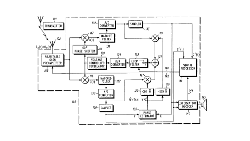
Figure 1 is a block diagram of a transmitter and
20 receiver which may employ the present invention.
Figure 2 is a block diagram of a signal processor
which may employ the present invention.
Figure 3 is a block diagram of an energy estimator
which may employ the present invention.
Figure 4 is a channel state diagram for a TDMA
event sequence which may employ the present invention.
~ 13 2071869
Detailed Description of a Preferred Embodiment
A system which may employ the present invention
is shown in the block diagram of Figure 1. The figure
5 shows a transmitter 101 and a receiver 103. The
receiver 103 comprises a carrier recovery apparatus for
~/4-shift DQPSK modulation. Receiver 103 elements
comprise a signal processor 141, an information decoder
143 and an adjustable gain preamplifier 105. All other
10 elements in the receiver collectively comprise a
decision feedback phase lock loop. The decision feedback
phase lock loop (DFPLL) generates a phase-error term at
the output of summer block 121 which corrects the
phase of the local estimate of received phase generated
15 by voltage controlled oscillator 109. The signal
processor 141 uses quadrature component signals, I'(t)
and Q'(t), and synchronous signal 144 to generate a
control signal 142 for adjustable gain preamplifier 105
and synchronous TDMA timing reference signal 140 for
20 the frequency response of loop filter 123. The control
signal 142 for adjustable gain preamplifier 105 is
adjusted based on the energy level of the received signal
102. The control signal 140 for the frequency response
of loop filter 123 is based on parameters of the received
25 signal. These parameters comprise: the energy level,
the rate of change of the energy level and the clocked
TDMA event sequence of the received signal 102. The
control signal 140 for loop filter 123 adjusts the
response time for the DFPLL. An adjustable response
30 time may improve the quality of the received
information signal 102.
The response time in a conventional DFPLL is not
adjustable during fading conditions. An adjustable
response time is desirable during fading conditions.
1 4 ~ 6 9
When the received signal is entering a fade, the energy
~--~ level of the signal is gets weaker thereby approaching
the noise floor. Under this condition, it is desirab!e to
slow down the loop response time by narrowing the loop
5 bandwidth filter. The narrow loop bandwidth filter
increases the signal to noise ratio for the received
signal. The slower loop response time enables the last
good received signal's phase-error estimate to remain as
long as possible before the next signal is received.
10 Likewise, when the received signal is exiting a fade the
energy level of the signal gets stronger thereby rising
higher above the noise floor. Under this condition, it is
desirable to speed up the loop response time by widening
the loop bandwidth filter. The faster loop response time
15 enables the next good received signal's phase-error
estimate to be acquired as rapidly as possible.
The response time in the DFPLL phase-error
correction system is dependent on the timing of the
clocked TDMA event sequence. There are times during
20 the TDMA event sequence when it is desirable to have a
fast loop response time such as when we first lock on to
a received signal. There are other times during the TDMA
event sequence when it is desirable to have a slow loop
response time such as when we are receiving a signal
25 which is entering a fade.
A TDMA transmitter 101 transmits a digital
information signal which is modulated on the l(t) and
Q(t) quadrature component signals described previously.
This information signal is broadcast to a receiver 103
30 which receives and demodulates the information signal.
As previously noted, the information signal may be
subject to random phase delays and multipath fading
which degrade the quality of the information signal.
,~
~ 15 2 ~ ~7 ~ 8 6 ~
The phase error in the received information signal
102 is denoted by le(t) and Qe(t). In receiver 103, the
information signal 102 is coupled to adjustable gain
preamplifier 105 which reduces input signal energy level
variations as discussed in Canadian Patent Application
No. 2,051,982 filed on September 20, 1991. The output
signal of
adjustable gain preamplifier 105 is subsequently
separated into quadrature signal components l(t) and
10 Q(t). Quadrature signal component, Q(t), is generated by
applying the amplified signal to a conventional mixer
107 where a local oscillator signal generated by VCO
109 is shifted by a fixed 90~ phase shifter 111 to create
the Q(t) signal. The l(t) signal is created from mixer
113 and the output local oscillator signal from VCO 109.
Quadrature signal components, I(t) and Q(t), are now
phase coherent with the transmitted signal.
Quadrature signal component, Q(t), is filtered
through matched filter 131 and subsequently coupled to
analog to digital converter 132. Digitized signal, Q(t), is
split into two paths. One path is mixed in mixer 117
with an estimated phase signal processed by sine
determinator 119. The other path is sampled by
conventional sampler 133 before being applied to a first
port of phase estimator 135, a first port of signal
processor 141 and a first port of information decoder
143.
Likewise, quadrature signal component, I(t), is
filtered through matched filter 137 and subsequently
30 coupled to analog to digital converter 138. Digitized
signal, I(t), is split into two paths. One path is mixed in
mixer 127 with an estimated phase signal processed by
cosine determinator 129. The other path is sampled by
conventional sampler 139 before being applied to a
2071869
-
16
second port of phase estimator 135, a second port of
signal processor 141 and a second port of information
decoder 143.
The resultant mixed signals from mixers 117 and
5 127 are coupled to a conventional summer 121. The
output phase-error signal of summer 121 is coupled to a
digital to analog converter 124 through loop filter 123.
The analog phase-error signal is applied to VCO 109.
VCO 109 generates a local oscillator signal to be applied
10 to mixer 113 and serially applied to 90~ phase shifter
111 first then to mixer 107.
Terms are described for the quadrature signal Q(t)
side of the DFPLL. The phase-error estimate signal of
summer 121 is generated by a comparator which
15 compares the received carrier signal phase (first input
to mixer 107) to a reference signal phase (second input
to mixer 107) generated by a reference signal source.
The comparator comprises: mixer 107, matched filter
131, AtD converter 132, sampler 133, mixer 117,
20 summer 121, sine and cosine determinator 119 and 129,
mixer 127 and phase estimator 135. The reference
signal source comprises: voltage controlled oscillator
109, DtA converter 124 and 90~ phase shifter 111.
Analogous terms may also be described for the
25 quadrature signal l(t) side of the DFPLL.
Signal processor 141 receives inputs l'(t), Q'(t) and
information decoder output 144. Signal processor 141
generates two outputs. The first output is a control
signal 142 for adjustable gain preamplifier 105. The
30 second output 140 is a control signal for the frequency
response of loop filter 123.
Information decoder 143 receives inputs l'(t) and
Q'(t) and generates outputs to the signal processor 141
and speaker 145. The information decoder represents
2071869
17
elements of a receiver not shown in FIG. 1. The first
output 144 to signal processor 141 provides information
about the position of a received signal 102 in the TDMA
event sequence. The second output 102 is an analog
5 output which may be coupled to a conventional speaker
145.
Referring now to FIG. 2, a block diagram of signal
processor 141 is shown. Digitally sampled signals, I'(t)
and Q'(t), are coupled to energy estimator 205. A
10 cellular radiotelephone transceiver in compliance with
IS-54 must determine an estimate of the energy level of
the received signal and process it in accordance with
Section 2.4.5.4.1.2.1. Further details on the function of
the energy estimator 205 will be discussed with FIG. 3.
The output of the energy estimator 205 is coupled
to adjustable gain preamplifier 105 using control signal
142, energy level detector 207, and rate of change of the
energy level detector 209. The output 142 from energy
estimator 205 to the adjustable gain preamplifier 105 is
20 a feedback path which reduces received input signal
variations.
A software process in the signal processor
determines the energy level of the received information
signal. The energy level determinator 207 can be
25 described by the following equation:
E(x) = 1 /(1 OVCtl)
where Vctl is the feedback signal 142 also used to
30 adjust the input gain to reduce input signal variations.
The output of the energy level determinator is
coupled to a limiter 211. Limiter 211 creates a
threshold level for high levels of received information
signals. Limiter 211 only allows measured energy levels
2o7l869
1 8
up to a maximum predetermined value. The output of 211
is coupled to product combiner 213.
The output of energy estimator 205 is also coupled
into a rate of change of energy level determinator 209.
5 The rate of change of energy level determinator
describes how the energy level of the received
information signal changes with time. In the preferred
embodiment, the rate of change of energy level can be
described by the following equation:~0
dE(x)/dt = dt1/10VCtl)/dt + K
The output of the rate of change of energy level
determinator 209 is coupled to limiter 215. Limiter 215
15 creates a low threshold for the measure of the rate of
change of energy level. 'The low threshold is set to a
predetermined value to prevent the calculation of rate of
change of the energy level from approaching zero. The
output of limiter 215 is coupled to product combiner
213.
The input 144 from information decoder 143
coupled to TDMA time clock 219 provides information
about the position of the received signal in the TDMA
event sequence. The output of the TDMA time clock 219
is coupled to look-up table 221. Look-up table 221
contains a number of predetermined values based on the
receiver design and location within the TDMA event
sequence. The output of look-up table 221 is coupled to
product combiner 213.
The product combiner 213 has as its inputs the
energy level determinator 207 processed through a high
threshold limiter 211, the rate of change of energy level
determinator 209 processed through a low threshold
limiter 21~ and a predetermined value from look-up
19
table 221 based on the clocked TDMA event sequence
.~~ 221. The product combiner 213 is a software process
which multiplies its three inputs to produce an output.
-The output of the product combiner is described by the
5 following equation.
(1/10VCtl) x (d(1/10VCtl)/dt + K) x (Value from lookup
table)
The output of product combiner 213 is coupled to the
loop filter 123 to adjust the frequency response time of
the loop filter 225.
In the preferred embodiment, the response time of
the carrier recovery apparatus is adjusted with a
1 5 variable
2071869
bandwidth filter. Adjusting the response time may also
be accomplished by varying the gain of the phase-error
signal coupled to a fixed bandwidth filter or by
averaging the phase-error signal over an adjustable time
period.
In the preferred embodiment, signal processor 141
is implemented as a digital signal processor (DSP)
employing a DSP 56001 available from Motorola, Inc. and
executing a series of preprogrammed steps to determine
the energy level of the received information signal, the
rate of change of the energy level of the received
information signal, and the position within the TDMA
event sequence. The DSP combines these parameters to
achieve an output which controls the decision feedback
phase lock loop frequency response time for loop filter
225. The DSP also produces an output to control the
adjustable gain preamplifier 105.
Now referring to FIG. 3, there is shown a block
diagram of the contents of the energy estimator 205.
Received quadrature component signals, I'(t) and Q'(t),
are coupled to averager 301 which calculates an average
signal energy from the addition of sample pairs of the
squared amplitude of l'(t) and Q'(t). The averaged output
is coupled to feedback gain adjust circuit 303 which
adjusts the value to which 1'2(t) and Q'2(t) are
normalized. The logarithm (base 10) is conventionally
taken (in 305) to produce the signal having logarithmic
characteristics to match the exponential control
function characteristics of the adjustable gain
preamplifier 105. The output of 1091 o (x) calculator 305
is coupled to voltage control sensitivity estimator 307
and mixer 309. The output of mixer 309, which
represents a control signal corrected for rate of change
of gain versus control voltage of the adjustable gain
~ ~ 7
21
preamplifier 105, is coupled to delay and compare
.- function 311. The output of delay and compare function
311 is coupled to control voltage sensitivity estimator
307 to correct for errors in the estimate of the rate of
change of energy level of the adjustable gain
preamplifier 105, and is also output to the other
functions of the receiver.
This output of the energy estimator 205 is
provided as an automatic gain control (AGC) signal to
adjustable gain preamplifier 105. The voltage control
sensitivity estimator 307 and the energy estimator 205
are further described in U.S. Patent No. .
5,083,304, filed on the same date herewith on behalf
of Cahill.
Now referring to figure 4, there is shown a timed
sequence of events for mobile transmit and receive
channels in a TDMA system. The mobile channel state
401 for a TDMA event sequence is generally divided into
three time slots. The three time slots comprise
transmitting (T) time slot 403, receiving (R) time slot
405, and idle (I) time slot 407. Each time slot is
approximately 6.66 milliseconds long thereby generating
a clocked sequence of events of 20 milliseconds for all
three time slots. The transmitting 403, receiving 405,
and idle 407 time slots are sequentially repeated in a
TDMA event sequence. As previously described, the
advantage of a TDMA is to multiplex the number of users
operating on the same frequency channel.
The idle time slot 407 defines a time in the TDMA
event sequence in which a particular mobile unit is
neither transmitting nor receiving. During this idle time
slot 407, the mobile unit intermittently measures the
energy levels of transmitters located in one or more
,, ~,
p,
2071869
22
cells. This process of testing signal energy level is
referred to as mobile-assisted hand-off or MAHO.
The mobile receive 409 describes the receive time
slots for three different mobile receivers described as
5 Rx 411, Ry 413 and Rz 415. Each mobile receiver can only
receive information during its allocated time slot.
The mobile transmit channel 417 is likewise
divided into three time slots. The three time slots
comprise Tx 419, Ty 421, and Tz 423. Each mobile unit
10 may only transmit during its own allocated time slot.
The transmit 417 and receive 419 channel pattern of the
three adjacent time slots is sequentially repeated over
ti me.
Note that the end of a transmit time slot for one
15 particular mobile channel does not line up with the
beginning of the corresponding receive mobile time slot.
In particular, mobile transmit time slot Tx 419 is offset
from mobile receive time slot Rx 411. This offset is
primarily needed to account for real world system
20 considerations such as propagation delay and the
physical distance between transmitting and receiving
units.
The values in the look-up table 221 and the
position within a TDMA event sequence help determine
25 response time. A position in a TDMA event sequence
defines a specific location in a time slot of a mobile
channel. When the TDMA time clock 219 encounters a
predetermined position in the received signal 102 a
value from the look-up table 221 is coupled into the
30 product combiner 213. Specific positions with respect
to time occur during the TDMA time frame when a fast
loop response time is needed and other times a slow or
intermediate loop response time is needed. A fast loop
response time is desirable immediately prior to the
2071869
-
23
receive time slot 405 in order to rapidly acquire the
phase-error and lock on to the received signal. During
the receive time slot 405 the loop response time is
determined by the energy level of the received signal and
5 the rate of change of the energy level of the received
signal. During the idle time slot 407, the control signal
to adjust the loop response time is minimized or
eliminated .
Thus, the quality of the received information
10 signal in a TDMA system can be improved in the presence
of fading by adjusting the loop response time of the
decision feedback phase lock loop. The loop response
time is adjusted based on the energy level of the
received signal, the rate of change of energy level of the
15 received signal and the timed sequence of events in a
TDMA system.
What is claimed is: