Note: Descriptions are shown in the official language in which they were submitted.
2072~-47
OP IICAL INTEGRATED CIRCUITRY
Back~round of the In-~en~on
Technlcal FYeld
Optical CilCui[l ~, as included in all-optical as well as electro-optical
5 integrated circuits, is characterized by high population density as well as efficient
operation of optical element~ - acdve and/or passive.
Description of ~e Prlor Art
Domin~nce. of optical tr~n.cmi.~sion for use in most high capacity long
t~nre systems is now well established. Concentrated effort both here and abroad
10 has resulted in expedient manufacture, inst~ tion, and use of fiber which satisfies
the motivating promise of high capacity, low loss tr~n.cmi.csion While not as well
developed, the status of medium and short ~ t~n~e is not very different. Active
backplane as well as microstrip media are on their way to satisfying needs.
For the most part advances in opdcal tr~n.cmi.csion have not been
15 matched in interfacing ci~uilly. Most operating systems rely on electronics for
interfacing with optical tr~n.~mi.csiol-- Mod~ tion of the optical carrier, generation
of optical signals to be inserted in the tr~n.cmi.~ion line, detection of such signals at
line terminals, amplification at repeater stations, etc. all depend upon electronics
rather than photonics. Equipment e~pen.ce as well as operating problems at
20 electronic-opdcal interfaces have provoked worldwide effort toward development of
all-opdcal equipluent.
While interfacing with optical tr~nsmi.~cioll systems is properly regarded
as the chief motivation, at least on the shorter term, inherent p~pellies of optics
provoke effort di~ected toward optical circuitry. The ultim~te ambition is all-optical
25 in terms of device filnction At this time, and probably for some time in the future,
con~enien~e of el~;honic biasing/pumping su~ges~ that CilCUill~ will take the form
of op~electronic integrated circuits. The likelihood that electronic elements will
condnue to be of choice for some funcdons ~uppo-~ this conclusion.
Circuit density has been a major concern in the development of optical
30 ICs - as regards both t~nsmi~ion paths and devices, e.g. ~ nplifiers, switches, etc.
Unwanted evanescent field coupling - a pheno,.,enon of little consequence in
electronics - imposes spacing limit~fions as between adjacent paths and devices.Effort directed toward opdcal IC chips to perform all but the simplest funcdons has
been thwarted by crosstalk and other consequences of un~an~ed coupling.
35 r ~ssening of such effects has led to spacings generally of tens of micrometers -
generally to tens of wavelengths as measured in vacuum. (The two spacing
-2- 2072247
mea~s are quite similar for popular operating wavelengths from =0.9 to l.S5~m
as available from popular GaAs and InP-based devices.) Use of design rules of
=lO~m would satisfy some short term conservadve objectives, but even at that level,
unwanted coupling, likely above =10%, is objectionable both in terms of noise and
S of energy/heat lissipation.
Summa~ of the Inven~on
In general terms the invention permits e~pP~içnt incorporation of optics
into ICs. Such integrated circuits may be all-optical or electro-optic but invariably
share close spacing and small size to permit high device density for a permitted level
10 of unwanted coupling. The md~t consequential effect of unwanted coupling is in
terms of Crosstalk - unwanted signal or "noise" as input into a circuit element
responsible for carrying signal information. The invention permits spacing/size as to
accommodate generally imposed noise restrictions. Most important embodiments, interms of either electro-opdc or all-opdc, are full functioning in the sense that device
15 inte~onnections are optic as are the devices themselves. Devices, which may serve
the various functi~ c of, e.g. signal ll~hspoll, Amrlification, and temporal as well as
spadal ~itching, are, to substandal e~ctent, inl~r~onnecled without electronic
interface in the signal circuitry. Electronics, to the e~ctent involved, likely serves
"support funcdons" such as biasing - either constant or intendonally varying - or
20 energizing - e.g. for l_ser pumping.
The essence has been stated - device size/spacing with lesser coupling to
permit "full functioning" IC opdcs. In ~plesentadve terms unwanted coupling - e.g.
as resulting in crosstal~ - may be mAintAinPd at a level of S 10% con~ n~ with
spacings of =lO~lm, or =5~0 for emission wavelengthc con~el~iehtly available from
25 m-v semicon~du~lor lasers.
Relevant opticA~ IC pordons whether conC~itnting part or the entirety of
the total IC, are, most i",pol~ntly, ch_raçteri7Pd by a funcdonal layer thickne~s
dimension (the dimencion orthogonal to the plane of the IC) of a maximum of a half
wavelength or preferably of a quarter wavelength for relevant prop~g~ting photonic
30 energy, with this limencion~ in turn, being m~int~inçd physically thin by virtue of
choice of materials to result in high-opdcal contrast in salient direcdon/s. Lowcoupling, high device density of the invention is made possible by inde~ contrast at
bounding device in~rfr~es - rado of IciLaclive inde~c values within and outside
relevant devices - numç~lly 1.5 or preferably higher. Permitted layer thickness
35 and other cridcal ~imen.cions are disc lssed in the Detailed Descripdon for usual
operation. For generally contemplated wavelengths the device-funcdonal layer
-3- 2072247
thicl~n~es is within the broad range of from 500A to a few thousand A - typically
from l,000A to 2,000A. Guide strength resulting from such specification permits
not only a spacing, device-to-device spacing, of approx 10Ao or less - even of
appro~SAO - while meeting noise requirements. In addition, reducing the energy
S fraction and field penetration depth into the surround, permits shorter radius of
curvature, thereby again adding to design fle~ibility to permit greater device density,
commensurate with given coupling crosstalk/loss.
It is an attribute of the invention that the device-functional layer may be
of proper composidon and dimension to serve for fabrication of devices of differing
10 functionality - active as well as passive. Briefly, contemplated devices may make
use of such a layer, in turn, constructed of sublayers. Such a "superlayer", in totality
of the ~hiç~ness specified above, may be made up of sublayers each constituting a
quantum well (as separated by barrier layers) e.g. in a laser structure. The same
superlayer, with or without modification, lends itself to - may even enh~n~e - other
15 operating structures. The term, "superlayer" is in~en-lPd to include superlattice layers
as well as Multiple Quantum Wells. Superl~tice structures, while similar, differ in
known res~cls to better adapt them to panicular devices. While detailed description
is not neces-~y here, a difference entails freedom of carrier modon - while carriers
are generally constrained to a particular QW of an MQW sl-u ;lu,t;, carriers are not
20 so cons~ained in a superlattice.
E~amples set forth include: guides which, themselves, may serve as
active elçmP~te- to couple or to decouple in accordance with a variety of controls;
controls depending on applied electric field or photons, e.g. to Q-spoil cavity
char~r~eristi~s reladve to ~ee~i~t~d elem~Pnts or to saturate and thereby "bleach" a
25 device material (as defined herein to include guide n-~teri~1) in this jn.et~n~e
O~l~g as a saturable absorber. Other e~camples include modification of refractive
inde~ to- injerted camers e.g. to alter leson~n~e frequency. Many other
control ,~ h~ -ic~ns are known and are contemplated.
Brief Descrip~on ot ffle Dl ... ~-..e
FlGS. 1-9 illustrate rep,~sentative 5lru~;lul~S usefully incorporated in
full functioning optical cu.;uil, y in accordance with the inventive teaching.
In general, die~ue~sion is in terms of specific noted attributes.
Ch~ teristics of devices mee~ing the inventive criteria permit design flexibility in
more general terms. For e~ample, device ~impncions - both orthogonal to and in
35 plane - and the high energy confinP-mPnt fun~mP,nt~l to the inventive tPaçhing - are
generally advantageous. The problem of "skew" - e.g. differing arrival times of
4 2072247
signals or signal portions to be simulLaneously processed - is addressable by sizing
and/or shaping signal elernP~nLc so as to delay or advance - so as to assure
simultaneous arrival. Variation in effective refractive inde~ due to signal-to-
surfacelinterface represenLs one apploach for accomplishment. Path length increase
5 by guide bending, as di~ ssed with reference to FIG. 1, rep~senLs another
approach.
FIG. 1 is a plane view of an element serving purposes including signal
transport. Whether passive or active it illustrates an advantage of the teaching in
permitting a tight bend of small bend radius as due to the strong guiding power of
10 the thin, highly inde~ contrast layer from which it is fabricated;
FIG. 2 depicLs a passive element providing for splitting of an incoming
signal to result in propag~tion in t~,vo guides;
FIG. 3 depicts an element physically similar or even i~entir~l to that of
FIG. 2 but providing for combination of two incoming signal streams;
FIG. 4 is again a plane view of a structure resembling that of FIGS. 2
or 3, and providing for the splitting of the former or the combining of the latter, with
additional provision of a control for switching or altering relative amplitudes during
operation. The structure shown may, accordingly, be "active" in accordance with
usage of that term in the present teaçhing;
FIG. S is a plane view of a ~LI~clu~, either passive or active, providing
for coupling or decoupling as between two ~dj~çent lines;
FIG. 6 is a perspective view depicting an illustrative embodiment of a
photon flu~ gene~ator. An included ~l~.u;lu,e of particular significance is the thin
film laser which, due to such thinnpss together with the inde~ contl~l common to25 other ~ e embo~imPn~, manifests the signal confinPmPnt to permit low
threshold lasing with consequences, e.g. in terms of ~impnsions and/or low noise,
opera~on as ~ s~ed in the Detailed De~.;pl;on;
FIG. 7 is a plane view schP-m^~ ly depi.;Ling an IC region providing a
laser such as that of FIG. 6 as combined with inputloutput lines and with control
30 means for coupling/decoupling;
FIG. 8 is a cross section~l view of a structure providing for coupling -
ev~nes~ent field coupling - of adjacent ehPmPnt~ as enh~nced by element-to-elernent
bridging as discussed further on;
FIG. 9 sch~Pm~ic~lly depicts a portion of an IC providing for selective
35 coupling - as to either or both of ainplitude and line choice - e.g., of signal em~n~ting
from a whi~pering mode recon~tor;
s 2072247
F~G. 10 is a perspective of a version of the invention in which the
conce .Rd optical IC portion serves as a "smart" interconnect between electronicICs/portions; and
FIG. 11, consi~ting of si~ cross-section~l views, FIGS. 1 la through 1 lf,
5 depicts sequential process steps suitable for fabrication generation of structures of
the invention.
Detailed Desc~ ion
Defini~on of Terms
To a significant e~tent, terminology used in the description of this
lO invention is that used in the telecommunirations industry. It is clear that the
inventive te~ching is applicable to a broader range of technologies - including other
forms of communication, private as well as public, computer, television, etc. Some
of these are ~ ssed by use of speci~li7~d terminology. The particular terminology
chosen in this description is, accordingly, not to be regarded as limiting
Signal - inform~tion e.g. as inputted to a con~e.. ~ed optical IC
portion in the course of device operation. Generally encoded, it may
include proce~ing instructions - the latter often referred to as "header".
The rem~inder of the signaL or the entirety if no header is included, is
sometimes referred to as a "data stream".
Con~ol Signal - information designed to modify signal with regard,
e.g. to path choice, path direction, ~mplitude, etc. as well as to change
intelligence content of the signal. Control signal information may be
introduced together with the data stream in the form of a "header" as
noted in the preceding paragraph. Alternatively, or in addition, control
signal inforrn~tio~ may be introduced separately, into one or more
elempnt~ within the body of the concerned IC portion. Control signals
may take any applopliate energy form - likely electrical or optical.
Crosstalk - as rigorously defined, the term refers to signal
inforrn~ion as imp~opell~ input e.g. into an active device or passive
device - by virtue of u~ ted coupling. Me~ningful design criteria
impo~ concel,- the e~tent to which such "noise" can be tolerated - a
level which for many pw~os~s is at the S 10% or preferably S% level (see
Detailed D~sc,iplion for further details).
The term "crosstal~" is often used in a less rigorous sense - in terms of
energy loss by the device yielding the crosstalk. This has consequence in
terms of possible need for amplification/regeneration. In terms of
-6- 207~2~7
unwanted coupling with apparatus not carrying signal information - e.g.
as generally true of the substrate, "crosstalk" has implicadons solely in
terms of energy loss.
Full Funcffoning Circuit - refers to circuilly~ circuit regions, circuit
portions in which signal processing is of a variety of forms. The
terminology as applied to optical IC portions is intended to include at
least three of the functions of: transport, redirection, combination,
splitting, modulation, and amplificadon. It is geneAc both to optical and
electronic circuitry, as well as to optoelecllonic circuitry.
FuU Functioning Opffcal Circuit - As above, but refers to such
circuit in which at least 95% of forms of signal proce~ing contemplated
is by means of active optical elPrnPnts, i.e. elem~Pnts of optical properties
varied by control signals. As otherwise noted, transport as between
optical devices in such circuit is usually - es.~enfi~lly invaAably - itself
optical.
Signal Cln;~ll~ - refers to that part of a functioning circuit, e.g. of a
fim~tioning optical circuit, accomplishing functions noted, e.g.
redirection, combination, splitting (or fan-out), modulation, amplification
and transport of signal being input. The term is intended to be
in~ependent of "support CilCUit~
Support Ct~t" - refers to circuitry responsible for operating the
signal ci,-;uil ~ - e.g. as control with regard to active elements -
,esponsible for signal procesing Fllnctiotl.~ of support circuitry include
biasing and energizing, e.g. pumping of an included laser or Light
Fmitting Diode.
Full Fw~oning Op~cal Integrated Ctrcuit or Full
Func~oning Op~cal IC - reference is made to the full functioning
optical circuit or circuit portion which is the primary objeclive of the
in~ ti~e te aehing. Depending on conte~t such IC may be all-optic, or
may include electronic ci cuil,~/e1Pm-Pnts as to cau~se or fi~ilit~tP optical
operation, e.g. design~Pd to ele~ onically pump or bias ~ t~Pd optical
circuit~y.
Devloe-Func~onal La~er - this refers to a m~Pri~l layer from which
devices are fabricated within which conce ~.rd optical energy is largely
confined This layer is initially deposited on a supporting surface - either
that of the primary substrate or of some interme~ ~ layer in turn
-7- 20722~17
led by such substrate. In some instances device construction does
not require retention of such supporting surface so that fabrication may
entail removal to leave an e~posed device-functional layer.
Contemplated fabrication variations may include bac~filling as by
S deposition to cover part or the entirety of the e~posed layer, likely with
material presenting ~i&nific~ntly lowered refractive inde~ than that of the
layer. Much of the descliption is in terms of a preferred embodiment
which depends on a single such layer for most or even all optical
e!ement.~ within the full functioning opdcal IC. Variations may depend on
more than a single ~lyer.
Passi-~e Element or Passive Device - an e!ement for inclusion in an
optical IC in which any change in photon flu~ - e.g. splitting, merging - is
due to unch~nging ch&~Lelistics of the element - pell-aps solely by
virtue of the character of the element; perhaps as affected by ancillary
biasing or other means. The prime e~cample is the simple element-to-
element optical guide - e.g. as connecting two active elements. Any
ch~nging characterisdc may be regarded as "noise" - is ~1nnecess~ry to the
IC functi~m Change such as due to effect of varying temperature is
nPcecs~- ;ly within device tolerance limits.
Acff~e Element or Acti~re De~ioe - an elrment affording means for
ch~nging some ch~cten~tiG for relevant photon flu~c during IC
operation. The term includes both element~ designed to generate/amplify
photonic energy - lasers - as well as those performing other IC functions
such as: mo~ul~ting; coupling-decoupling; splitting/combining;
~wi~Lng, etc.
'~nn is the leî~ ive inde~c for the particular wavelength of photon
flwc conee ..rd - as related to that in vacuum. Co~lsi~ten~ with general
usage the term has reference to the bulk value of ~e~a~;~ve inde~c - i.e. the
n;fi~li~ inde~c for such wavelength as measured in a body of uniform
composilion and of infinite size (to avoid alteration of value due to flu~-
surface interaction).
"n D " - iS the average value of bulk ~efr~;live inde~ for the device-
fimctio~ layer. In in.~l~nceS in which the device-functional layer is of
varying inde~, e.g. as in a "superlayer" (con~ d of sublayers of
differing ,efiaclive inde2~), the term rep,csents an "average" - i.e. the
inde~ "seen" (the inde~c value e~planatory of observed action) by photon
-8- 20722~7
flw~ traveling in a given direction within a body of inde~ n D. in which
inde~ value is unaffected by interacdon with bounding surface/interface.
"ns" - is the bulk l~fi~ ive inde~ for the material/environment
bounding the device-funcdonal layer. As in the definifiQn of nD the term
may rep~escnt a weighted average in the inct~nce of local variation in
inde~.
A - wavelength of concemed photon flux generally expressed as such
value in vacuum, ~0.
Ao - wavelength of concemed photon flux as measured in vacuum.
lndex Contrast - rado of refracdve inde~c values as between the
device-funcdonal layer and surrounding m~teri~l in terms of the rado
n D/n s . in which n D and n s are as defined above.
General
The inventive impact has been ~ cuc.c~d in the Summary. Advantages
15 implicit in use of photons rather than electrons have provoked prior effort as well as
the work res~lting in the present inventdon. One such advantage concems the factthat photons, unlike electrons, are uncharged. This fact gives rise to circuit
app,ua~hes that may be of value. As an e~ nplP integrity of photon flwc direcdon is
unaffected by pro~imity and even by crossing - by local usage of the same funcdonal
20 device region simultaneously by two defined flows.
The in~ ..live teaching o~te~o",es what is perceived as the main
obstacle to re~li7~tion of such advantages as well as to more general use of
integrated optdcs. The invention addresses difficulty conce".ed with an implicitdirÇe~nce as bel-.~n photonics and electronics. For d;...~ncionc contemplated - for
25 micron device ~limPncionC min~ ri7~tion of electronic Integrated Circuits is not
in p~ciple, compli~ ~ed by ull~ ted coupling due to imperfect guiding. In simple terms, d:~le~-l- ;c con~ as bel-. en electronic conductor and in.C~ tor is very large
cûmpa~ed to the available inde~c contrast for photons. Device rlimencion and device
spacing ~ t~inP~d in elce~nic ICs at both present and now-contemplated design rules
30 have prim~rily con~ ..cd fabrication. Design rules have de. ,eascd apace with: e.g.
improved lithographic definiti-)n as afforded by decreased wavelength of delinPa-ing
r~ ion; and a variety of p,~lical problems conce~,fiing image registration, etchremoval, controlled diffusion, etc.
Miniaturi_adon of photonic Cil~;uil~ is complir~ted by signific~nt field
35 penetradon through the interface between device and ~u"ùund - in simple
tr~ncmi.csion lines (generally, in passive devices as well as in the whole variety of
-9- 20722~7
active devices. This consideration, one with little analogy in electronics at present
dime- c:~nc, results in the whole variety of unwanted coupling effects - including
crosstallc as well as other forms of noise, and energy loss. The latter is a further
problem due to absorption accompanying hP~1ing
The major thrust of the invention depends upon the very significant
increase in guiding strength for optical signals which is a consequence of two
contributions both relating to the nature of the layered material from which elements
are fabricated. The first of these requires a layer thickness, T, of a ma~irnum of
"1/2A" in accordance with the equation:
T S
2~n2 _ nS
This maximum permit~ed layer thickness subst~nti~lly assures single mode operation
- to lessen crosstallc/loss likely larger for higher order modes, and to lessen mode
dicpçrsion which might otherwise limit ope.aling frequency. While some mode
conversion will occur, its likelihood is reduced by limiting funcdonal layer 1hi~n~ss
15 to this n 1/2 A" value or less.
For many purposes a preferable layer thic~ness is "1/4A" wavelength:
T Ao
4~nD - n2
The second contribudon chala"t~ ing the invendon requires a
subs1~nti~1 inde~c cor ~ as be~v/een the device fun~tion~l layer and the surrounding
20 medil-m E,-~lessed as the fracdon nD/nS, ~lluclu es of the invendon require a contrast of at least 1.5 and preferably greater.
Contrast rados greater than 1.5 further advance the invendve thrust
depending upon errccLi~le confineme-nt and are, therefore, plefe..~d. Available
m~terisl~, o~,.wise suitable for surround, permit such greater values for devices
25 operating at typical m-v and II-VI wavelengths. For example use of silicon nitride
may re~wlt in cont~3st of = 1.65. Other materials may result in a conl-~l of 2 or
more - SiO2 ~wlound may result in contrast of 2.3. Of course, air, other gaseousenvilo.. rnts, or ~uu-u may result in nD/nS values in excess of 3 (e.g. - 3.5).
As suggest~ most circumst~ ~cP,s dictate a preference for the " 1/4 ~"
30 th~ ne~e. as defined above. There are, however, circumet~nces under which
so.newhat thinner layers may be tolerated or even p,e~elled. Such thinner layersinherent~y e~clv~1e a ~hinness-depen~erl~ inweasing fracdon of photon flwc - to result
in increased amplitude of evanescent field outside the layer, and, conseq~ently, in
increased pl~pensity for coupling. With regard to such layers to be fabricated into
2072247
- 10-
devices of larger spacing or with regard to such spaced devices as permitted within
local circuit regions, guiding is, to first approximation, the same. To large extent,
such further thinning appreciably beyond " lt4 ~" is limited by demands placed on
fabrication. As presently contemplated, dictated by practical considerations, layers
5 thinner than =" 1/8 A" are not likely to be used. Such a " 1/8 ~" layer is, consistent
with the above, defined in terms of:
T- ~o
~ n2 _ nS
Note - Above ~iccu~ion relating to values of "T" is in terms of a fundamental thrust
of the invention in accordance with which spacing is reduced while keeping coupling
10 to a minimum. As in other integrated circuits, there are positions at which coupling
is wanted - is wanted to effect e.g. connection. The same considerations may be
involved in this desideratum. Reduced thi~L-ne~ss for prop~lly spaced devices, in
res..l~ing in e~cluded flu~, may design~Pd1y increase such wanted coupling.
It is recognized that the above equations are not rigorously derived. For
15 e~cample, they depend upon "bulk" values of inde~c - both as within the funcdonal
device layer and its sullound. Such bul~ values are not precisely desclip~ e of most
forms of devices constructed in accof~ance with the invendon - devices constructed
of funcdonal device layers in which ~hicL-n~p~ may be such as to have significant
effect on refracdve inde~ (as to alter inde~ due to intef~ ion as bel~een photon flux
20 and surfaces/inte~f~es - as further aggravated by any deviadon from perfect surface
smoothness). Further design may, as noted, deliberately entail inde~
inhomoge~ne;l;~s - e.g. as due to layer-to-layer v~ri~tion~ within "superlayer
structuresn, or as due to graded inde~c. Use of weighted averages as provided for,
while improving the applu~ tionl does not, in itself, yield rigorously precise
25 values.
E~Li~e study and e~perimp~nt~tion s~tisf~ctQrily support use of the
equadons pl~senled for reliable tr~nCl~tion of the irl~,nli~e te~hinR into structures
which share the advantages taught, Accordingly, while the "1/4 ~" value of T is a
con~c ~ient measure for pu,poses of design/f~bncation, the value yielded by the
30 equadon is only applo~ullately correct - the precise !hi~ L ..P-ss value of T for the
"opdmum" layer may vary - within the = ~ 10% range. As in~ic~ted. criteria as sopleser.t~d invariably result in advantages upon which the invendon is based.
The same considerAtions - subst~nti~l energy confinPmen~ due to
prescribed layer ~h;rL~css - tr~n.~l~tes into useful device plopellies, pardcularly for
35 devices of smaU lateral dimPn~ions cot-templ~tP(I Devices of least dimension less
11- 20~72247
than 20~m - likely smaller - operate effectively due to this quality. Contemplated
minimllm dimen-cion as small as ~ l/3Ao share the energy efficiency fundamental to
the invendve te~ching to result in low needed input power. This is true of
amplifying as well as other acdve devices, and of waveguides and other passive
5 devices. An important consequence of lowered input power is lowered dicsipation -
to reduce e.g. unwanted hPating. Studies establish feasibility of device operadon at
< 100 microwatts dissipation/device averaged over such devices as included in a full
funcdoning optical IC portion herein.
The invendon is described in terms of most salient features - in terms of
10 design fle~cibility and noted advantages as resulting from the highly efficient energy
confimPmPnt afforded by thin full functional device layers ~iccuc.ced Descripdonwith regard to composidon is largely in terms of m-v and II-VI-based m~teri~lC of
present in~erest. The inventive tPa~hing is advantageously applied to any such
materials, but is not to be so restricted. Invendve lequil~"lents are in such terms as
15 to be directly applicable to other materials - even to as-yet uni~ntifiP,d m~tPri~lc.
Pardcularly with a view to inclusion of light generadng devices, there has been some
emph~cic on semiconductor materials of direct b~ndgAr. For many contemplated
purposes, indirect bandgap m~tçn~ls may serve - for specific purposes perhaps
advantageously. Variadon in m~tPn~l plopellies, as yet unrealized, may permit use
20 of the invendve approach - as an e~ample, effort directed toward modification of
silicon to permit sdll broader use, perhaps to convert its band ~llu~;lule or to introduce useful light-gent;,~ing prope~lies by doping, may be ~uccessrul.
The In~entive Product
It is con~eniellt to discuss concç ..ed integrated opdcs in terms of the
25 Sgures. Full filn~!inn~l optical IC portions Ch~."~ ~r Azed as above - in terms of, e.g.
fun~ tio~ layer Ihi~ L~CS.5, inde~c/indices, device ~imencions~ device spacing - are
here defined as including at least 100 opdcal elemçntc (at least 100 opdcal devices)
meedng the ill-e~ criteria of thi~ness and inde~c contrast. Full funcdonal opdcal
IC portions may include additional cilcuiîl~ - may include elem~ntc which do not30 meet the inventive cdteria They may include e.g. opdcal elemPntc of greater
thirl~necs (of thicl~nloss of one or many wavelengths as defined), as well as non-
opdcal elemen~c - e.g. electronic elementc and/or co~ductor.c, some likely serving
fun~tionc of support Cil~;uill~.
FIGS. 1-10 conctitute a ,~pl~senlative "catalog" of elementc and
35 subCil~;uiLS m~eting the invendve cAteAa
20722917
- 12-
FIG. 1 is illustradve of a category of elPmentc - con.ctituting passive or
active devices - lilcely included in a full funcdoning opdcal ~C portion. The
particular element 10 provides for transport of photon flux and resembles a ridge
waveguide. It may have relatively tight bends - e.g. 5 Ao or less for tolerable loss -
5 as at 11, 12 and 13, as permitted due to the thin device functional layer of whichrelevant devices are constructed. For optimal thi~lrness~ for "quarter wavelength"
thiclrn~Pss, a bend radius of 2Ao - e.g. 3~1m - results in a loss of less than 1% 90
bend (for flu~ wavelength of ~0 =l.5~Lm). While li~ely serving as a simple passive
lran~ elPment it may serve additional functions as well. For example, optical
10 pumping, by means not shown, may saturate the guide 10 to lessen insertion loss -
e.g. to "bleach" a laser composition or other absorbing me-lium Such optical
pumpmg may be constant, or it may be altered in amplitude, either condnuously orstepwise. In accordance with Definition of Terms, the e!ement shown would then be
cl~c-cifiPd as "active".
FIG. 2 provides for splitting or "fan-out" as between incoming signal 20
and outgoing signals 21 and 22. The acdon is a consequence of coupling between
guides 23 and 24. For contemplated materials and limer~.cions as discussed, a
spaeing of appro~cimately 0-5~O for an u~t~lion length 25 of SAo, results in
approximately 45% of incident signal in each outgoing guide. The same flu~c
20 division is obtained for closer spacing and shorter inlelælion length or for further
spacing and longer interaction length.
As indic~tPd here and else.. l,e.~, perrni~d close device spæing is a
signific~nt cons~u~nce of the pronounced energy confinemm~ associated with the
thin device f~.r..-l;Qn~1 layer. Where needed, spæing and/or crosstalk may be further
25 reduced by provision of a metal barrier ~t~.~,e~l such devices. Cost of e.g. a metal
film of el~ en~ minllm may be justifiPd at least in specific positions on the IC,
under critical cirCllm~t~nr~es~
F~G. 3 depicts a passive element providing for merger of incoming
signals 30 and 31 as introduced l~spe.;~ ely into guides 32 and 33 to result in
30 combined output signal 34. Coupling æ to æsure -15% of the totality of the flux
introduced into both of guides 32 and 33 is æsured by spæing of 0.5 ~O, ~suming
single mode op~ratirJn As in FIG. 2 des.;,i~lion, the contemrl~ted interaction
~lict~nre of =5 ~O may be shortened or lengthened while ret~ining coupling strength
by le~peclively reducing or increasing coupling spa~ ing
2072247
The active device of FIG. 4 provides for control means shown
schematically as 40. The control means provides for, e.g. electronic or photonicenergization to modulate coupling as between guides 41 and 42. Performing as a
5 combiner, incoming signals 43 and 44 are controllably merged to result in combined
output signal 45. Performing as a splitter, incoming signal, shown as broken arrow
46, may result either in the entirety of the detectable signal exiting as 47 or,alternatively, in part of the flux exiting as signal 48.
FIG. 5 provides for coupling as between input signals 50 and 51 in guides
52 and 53. Control 54, again likely electronic or photonic, may permit or preclude
coupling - may modulate amplitude resulting from coupling ultimately to switch - to
result in output signals 55 and 56 of content/amplitude as so determined.
Alternatively, physical omission of, or constancy of input to "control" 54 may convert
the depicted structure so that it performs as a passive element. Performing as an
active element, consistent with the "on-off" logic of prevalent modern electronics,
control element 54 may selectively determine detected states in which effectively
either: amplitude/content of 55=50 and 56=51 or; 55=50+51 and 56 is cancelled.
The structure of FIG. 5 may serve as a two-by-two switch in which input
as 50 or 51 may be made to exit at 55 or 56. Arrays of such switches may increase
input/output lines so that, e.g. an 8x8 array may operate as a sixteen-by-sixteen
switch structure. Arrays of this nature are illustrative of simple forms of the
invention likely to find relatively near-term use. They may serve, for example, as
interconnects, e.g. in lieu of the particular full functioning optical IC portion serving
as interconnect for ICs 102 and 103 of FIG. 10.
FIG. 6 is illustrative of photon flux-generating devices suitably included in
optical circuitry of the invention. The flux confinement characterizing devices
fabricated from the thin device functional layer is of particular value in terms of such
devices. Improved efficiency and/or fabrication simplification is of consequence in a
large class of such devices including lasers, e.g. whispering mode structures asdescribed in U.S. Patent No. 5,343,490 that issued on August 30, 1994, as well as
cavitating structures operating below threshold - structures sometimes referred to as
superluminescent diodes. Improved guiding power constrains emission spreading
from simple LED structures, and so improves their functioning as well.
- 14- 2072247
FIG. 6 is intended as e~plicitly rcp-csentadve of a simple structure
d~pen~ g upon but a single standing wave - in contradisdncdon to the whispering
mode structure. Both types of structures have characteristics - fabrication as well as
perform~n~e - such that neither is precluded for IC use. Structure 60, while not so
5 limited in operation, is ~icsussed primarily in terms of a recdlinear lasing device for
operation above lasing threshold. As depicted, it consists of acdve gain region 61,
e.g. of suit~bl~ m-v composidon sandwiched be l~n layers 62 and 63, the three
layers together constituting the "device-functional layer" common, as unmodified or
modified, to most or all other devices - active and passive - within an optical ~C
10 pordon.
While dçt~ilPd discussion is not merited, pracdce of a preferred
embodiment providing for fabricadon of most, or even all, devices to be included in
a full fun~tioning opdcal IC, may usefully contempl~te perforrn~nre or fabricadon
where the device functdonal layer is to include flwc-gçn~rating elçment.~ Under
15 cl~sir~l condidons, use of laser-specified material in other elements operadng
below lasing threshold may result in intolerable loss for tr~n~mitting signals. One
soluti- l- provides for altering the bandgap of non-lasing e1~men~ m~teri~l e.g. by
diffusion. Another approach depends upon oper~ting cQn~ition~ to result in la~ser
output at a wavelength which does not coll~spond with the full m~teri~l bandgap.20 An e~cample involves "bandgap shrink~ge" to result in increased wavelength from
laser ele~n~ ~s Another involves ener~ t;on of non-laser m~ l to alter its
b~ndg~ - e~camples include ele~;l,onic biasing to shift quantum well state energies.
Still another soludon involves saturadon or "bl~ching" by direct current biasing.
Requisite inde~ cont,~l - as bel~en e1cposed sll~f.~es of structure 60
25 with s~ ding ..~e~i;v~l 65 - as di~ sçd - permits small layer thickness for given
fr~rtiorol A layers - e.g. for the ma~imum half wavelength or preferably quarter~a~el~Ab~ di...- n~io~ of pardcular value for cavitation. Field confineme~t increa~se
tran~lates into declease in laser threshold value.
While other fabricadon approaches are s~ti~f~-tQry, the use of a pedestal
30 64 of reduced cross secdon as interfacing with structure 60, permits air or vacuum
interface, to m~imi7e inde~c contrast at e~cposed surfaces of layers 62 and 63, in the
manner of the whispç~ng mode micro-resonators of the copending applicadon. The
strong guiding prop.,~lies bring about re~ tio~ in needed reflecdvity for the Fabry-
Perot ~llu.;lulc; (structure 60). For illustradve pul~oses, reflecdvity is provided by
35 distributed feedback regions 66, e.g. as conslin"ed of grooves 67 posidoned at usual
Distributed Bragg Reflector spacing, e.g. half wavelength spacing. Design criteria
- 15- 2072247
for such structures are well known - see for example G. P. Agrawal and N. K. Dutta,
LonR WavelenRth Semiconductor Lasers, Van Nostrand and Reinhold Company,
NY, (1986). Suffici~pn~ reflecdvity for laser action for IC dimen.ciQns contemplated
may requWdepend on metal coating, not shown, e.g. a coating of gold or aluminum
S on the outer surface of an in~.~lening low inde~c material, not shown, e.g. on SiO2
with such coating encompqc-cing a ~lluc~we length of several wavelengths (thereby
permitting 90+% reflectivity). The structure of FIG. 6 is in~ended as representadve of
elemPrltc operating below lasing threshold as well - a variety of circuit functions may
be performed by use of ~upe~lu~..ine~P~nt diodes with resulfing saving in fabrication
10 cost/yield. Flu~-generating sl,u.;lw~s may be light pumped, e.g. by separate laser
structures - as included on the same plane with or on a plane adjacent to that of
signal circuitry, or, alternatively, may be based on electrical pumping by means not
shown. Fmic~ion, e.g. as l~p~æn~d by arrow 68 may be in-plane, to permit
e~pedient coupling in the manner of that of usual edge-emitting structures.
FIG. 7 is a schemq~ir ,ep,~sen~q-l;on of a part of an optical IC portion of
the invention. Shown are: flu~ generator 70, e.g. Iaser 60 of FIG. 6, sandwichedbe~..~n guides 71 and 72. In the e~cample shown, coupling strength as between
guide 72 and flwc generator 70 is controlled by control 73 which may e.g. permitmodul-q-~ion of coupling strength, or may decouple guide from generator in the
20 abænce of a control signal. The figure is ep,esenlative of a large number ofvariations, providing for, e.g. change in flwc flow direction, as well as equipment
variadons e.g. eliminq~in~ or inc,e~sing number of control elPm~Pntc.
FIG. 8 is a sectionql view, most impo,~nll~ depic!ing an effecdve
means for coupling e4~ n~s 80 and 82 in separated region 83. In the structure
25 shown, e1empntc 80 and 82 were fabricated by etch sep~alion of a single device
func~ional layer, to result in separadon region 83, p~lhzps with separadon of spacing
of ~O, for the center wavelength of co~cern~Pd photon flwc. Bridging of region 83
by silica or other e ~c~ul~,ting m~Priql 87 is e~reditiously accomplished by
Chen~i~ql Vapor Deposidon. Alternadvely, a~sl)ming availability of material to suit
30 specific objectdves, such bridging may be the consequellce of wetting of material of
suitable free energy/viscosity prop~l~ies - followed by soli~ific.,tion as by freezing or
solvent removal. There is suffi~ient variety in suitable bridging processes as well as
materials to impose little constraint on composidon choice for pedest~ls 84 and 85,
and for substr~e 86.
20722~7
-16-
Silica is an example of a class of materials of ~ppropl;ate performance
characteristics - e.g. transparency - as well as fabrication characteristics - e.g. Iow
deposition temperature. The neck-down dimension may be of thickness comparable
5 to the device-functional layer or may be otherwise to serve a particular need. Since
the nature of this neck-down region, as CVD produced, is such that it necessarily
varies in cross-section to attain a minimum at a position spaced from facing surfaces
of guides 80 and 82, and since, in any event, it is relatively short in the flux traversal
direction, size is relatively non-critical.
Use of thin functional device layers in accordance with the invention
impacts wanted coupling efficiency. Required precision, particularly as to placement
of elements on a common plane, is expedited by approaches such as that of FIG. 8.
The bridge coupling illustrated takes advantage of common planarity of devices as
fabricated from a common layer. Contemplated circuitry may, however, be best
served by devices on differing planes. The essence of evanescent field coupling does
not require common planarity, but only requires sufficient proximity - a requirement
generally satisfied in terms of spacing of~1/2A~0. Plane-to-plane coupling may be
accomplished due simply to such proximity, or may be expedited by properly
positioned deposited material, e.g. SiO2 to result in vertical bridging analogous to that
shown.
FIG. 9 is a schematic representation of an IC region, in turn, part of a full
functioning optical IC, which may be implemented through the use of a whisperingmode resonator, e.g. a disc resonator 90, generically described in the above-identified
United States Patent No. 5,343,490. For the example shown, an input signal 91 asintroduced in transport element 92 (depicted as a passive element) is introduced into
disc 90. Control 93 may perform coupling-decoupling function for such introducedflux or, alternatively, may control operation of resonator 90 - e.g. to discontinue
operation or vary amplitude. Resonator 90 may be pumped by electrical or opticalmeans not shown. Introduction of emitted signal from resonator 90 may be into
either or both of guides 94 and 95 as determined by controls 96 and 97 to, in turn,
result in output signal at either or both of output positions 98 and 99.
Control elements in the structure of FIG. 9 as well as in other included IC
portions may depend on any of various mech~ni~m~, e.g.: quantum-confined Stark
effect, saturable absorption, phase space filling, etc.
~ ,~
- 17- 2~2~7
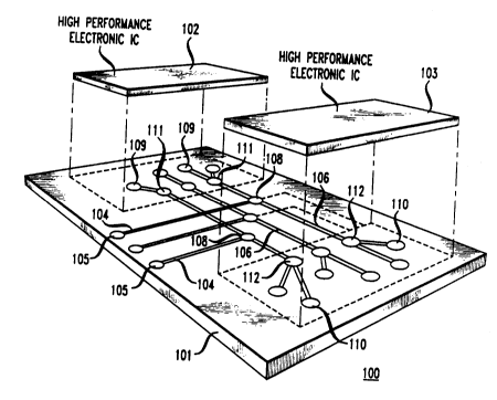
The apparatus of FIG. 10 shown in pe~pecti~e, and with parts separated
for ea~e of descripdon, is representadve of a likely near-term use of the invendve
teaching. While of more generic applicability, the relevant full functioning opdcal
IC portion 100 as constructed on substrate 101, itself a part of device-funcdonal
5 layer in common with other full funcdoning opdcal IC pordons of the invendon,
serves as a "smart" in~.connect as between high-perform~nce electronic integrated
circuits 102 and 103. Details of the opdcal IC pordon 100 are elsewhere discussed
and are not shown here. Briefly, the depicted e~ample provides for coupling of
guides 104 to opdcal fibers not shown at coupling points 105. Selecdve coupling of
10 input signals into guides 106 of opdcal bus 107 is controlled by opdcal switch logic
by means not shown at junctures 108. Opdcal-to-electric~l conversion, designed to
interface with contacts not shown on the undersides of ICs 102 and 103, is made at
eleme-nt~ 109 and 110. Fan-out, likely with path choice as det~PrminPd by opdcalswitch logic, is det~l...ined by operadon of elPments such as 111 and/or 112.
While wholesale substituti()ll of photonic ICs for electronic ICs is not a
near-term likelihood, advantages of the "smart inte~oMect" of FIG. 10 may suggest
early use. Electronic in~lconnecl;on of electronic ICs such as 102 and 103 of
FIG. 10, while acceptable at clock rates of ~ 1 gbit/sec., are a problem at higher
speed. ~esenlly ~ssl~med need for resistor shundng - e.g. - 50 ohm - to avoid
20 perforrn~nce-limiting reflecdon becomes a problem at higher speed - certainly at ~
10 gbit. Perform~nce limit~tion is a consequence of car~i~n~e-limiting loss for
usual in~l~;onnccl length in e~ccess of = millimeter order. Opdcal circuitry is not
similarly limiting
Fabricatlon
Various known fabricadon techniques are suitable for construcdon of
full fil~til~ning optical ICs and ancillary apparatus described. Operadon at "optical"
wavelengths imposes requirements e.g. in terms of surface/interfa~e smoothness as
well as compositisnsl precision and uniformity, etc. The 1/2~ layer ~hi~ness
m~-im--n commo~ to full funcdoning opdcal ICs of the l ?-hing impose further
30 constraints. S~ f~tion of such requirements, depen~ling on det~ilP-d considerations,
requires pl~C7~liotlc with regard to such chara~ t~ ;s~i~s as: crystallinity - e.g. with
regard to surface pre~nted for etching; freedom from voids in the inst~nre of
polycrystalline surface to be ploces~d; and attendon to telllpela~ uniforrnity as
well as uniformity of other proces~ing-relevant condidons, etc.
20722~7
-18-
Fortunately, epitaxial growth techniques, e.g. Metal Organic Chemical
_apor Deposition and Molecular Beam Epitaxy are sufficiently advanced to permit
reliable growth of the several hundred A thick and thicker layers thus far studied.
S FIGS. 1 la through 1 lf illustrate a typical processing sequence useful in the
generation of a highly confined optical microstructure of the invention. The
particular structure shown is suitable for operation at ~0 = 1.55~m. It involvesMOCVD growth on an InP substrate 120 of: 200A InGaAsP layer 121; 100A InGaAs
layer 122; 200A InGaAsP layer 123; and finally 200A InP layer 124.
In FIG. I l a, a 1200A thick Si3N4 layer 125 has been deposited by
MOCVD.
In FIG. I lb, layer 125 has been photolithographically patterned to yield
masking region 126. Desired dimensions of the order of one or a few wavelengths
(as measured in vacuum - ~0) may depend upon short wavelength delineating
radiation, e.g. accelerated electron radiation as described in U.S. Patent No. 5,130,213
that issued on July 14, 1992 or ringfield scanning x-ray as described in U.S. Patent
No. 5,315,629 that issued on May 24, 1994.
In FIG. l lc, the layered structure has been etched by Electron Cyclotron
Resonance to the depth indicated thereby yielding the columnar body atop partially
etch-defined InP.
In FIG. 1 ld, the masking Si3N4 layer has been removed in CF4 plasma.
Selective chemical etching of InP - of region 120 using an aqueous HCL
solution has yielded reduced cross-section column 127 as shown in FIG. 1 le.
FIG. 1 lf depicts a final element as encapsulated in layer 128 of a 0.5,um
thick layer of Chemical Vapor Deposition-grown SiO2. This figure is illustrative of a
general approach designed to lessen free surface carrier recombination. Layer 128
serves as an example of what is sometimes referred to as a "regrowth" layer - a layer
of epitaxially grown material of increased bandgap relative to the free surface on
which grown. Good quality epitaxial growth serves to effectively avoid
recombination on defects or other recombination centers. Increasing bandgap in such
regrowth layer prevents penetration of carriers to result in similar recombination
problem on the new free surface presented. SiO2, in presenting a larger bandgap than
illustrative materials of layers 121-123, if of sufficient epitaxial quality, e.g. to
minimi7e likelihood of voids, may serve. Good epitaxial growth, ~sllming needed
crystallinity match, is advanced by clean substrate surface-assured by etch-cleaning.
~ i