Note: Descriptions are shown in the official language in which they were submitted.
4
TITLE OP 'fHE INVENTION
Variable Delay Device
BACKGROUND OF TEiE INVENTION
Field of the invention
The present invention relates to a variable delay
device. More specifically, the present invention
relates to a variable delay device which is utilized as
an analog IC delay line.
Description of the prior art
Up to now, there is a variable delay device which
is constructed by using a C-MOS inverter. The C°MOS
inverter has a transfer delay time of approximately few
nanoseconds for each stage, and therefore, if the number
of stages of the C-BIOS inverter is increased, it is
possible to obtain a delay time equal to the number of
stages. The delay time of the C-MOS inverter can be
adjusted by a driving voltage which is applied to the C-
MOS inverter. In general, a control characteristic
2U representative of a relationship between the driving
voltage and the delay time becomes a non-linear
characteristic as shown in Figure 6.
In such a variable delay device, it becames
difficult to properly control the C-MUS inverter because
the control characteristic largely varies due to
- 1 -
dispersions or variations of a temperature, circuit
components and etc., and accordingly, there was a
problem that a characteristic of the variable delay
device does not become stable.
SUMMARY OF 3't1E INVENTION
Therefore, a principal object of the present
invention is to provide a variable delay device a stable
characteristic.
ZO The present invention is a variable delay device
comprising: a variable delay circuit including a first
variable delay line which is constructed by utilizing a
C-MOS inverter and delays an input signal and outputs a
delayed signal; and a correction circuit which applies a
first and a second outputs for respectively controlling
a linearity and a variable range of a control
characteristic of the first variable delay line.
On the basis of the output of the second and the
third variable delay lines included in the correction
circuit, the first output by which the control
characteristic of the first variable delay line is made
substantially linear is applied to the first non-linear
circuit from the linearity detecting means. An
input/output characteristic of the first non-linear
circuit is changed by the first output, and then, an
_ 2 _
~~y~~e.D~'~
output obtained by modifying the first control signal
which is applied to the first non-linear circuit is
given to the first adder. On the basis of the outputs
from the second and the third variable delay lines, the
second output by which the variable range of the first
variable delay line is made constant is applied to the
first adder from the reference level generating means.
The output of the first non-linear circuit and the
second output are added to each other by the first adder
and an added result is applied to the first variable
delay line. Therefore, the linearity of the control
characteristic of the first variable delay line and thus
the control characteristic of the variable delay device
becomes good and the variable range becomes constant.
According to the present invention, it is possible
to make the linearity of the control characteristic of
the variable delay device be good and to easily obtain
the variable range being made be constant always without
dependent on a temperature and etc. by the first and
second outputs from the correction circuit,
respectively, and therefore, even if the variable delay
device utilizes a C-MOS inverter, a stable
characteristic and a constant variable range can be
obtained.
The above described objects and other objects,
- 3 -
..-.~
features, aspects and advantages of the present
invention will become more apparent from the following
detailed description of the present invention when taken
in conjunction with the accompanying drawings.
BRIEF DESCRTPTIUN OF THE DRAWINGS
Figure 1 is a block diagram showing one embodiment
according to the present invention;
Figure 2 is a circuit diagram showing examples of a
ZO linearity detector, variable range detector, and
reference level detector utilized in Figure 1
embodiment;
Figure 3 is a waveform chart showing signals of
respective portions of a correction circuit constituting
Figure 1 embodiment;
Figure 4 is a graph showing an input/output
characteristic of a non-linear circuit;
Figure 5 is a waveform chart showing signal as of
respective portions in the circuit diagram shown in
Figure 2; and
Figure 6 is a graph showing a control
characteristic of a variable delay line.
DETAILED DESCRIPTION OF THE PREFERRED EMBODIMENTS
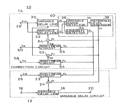
With reference to Figure d, a variable delay device
_ 4 _
of this embodiment shown includes a variable delay
circuit 12 and a correction circuit 14. ~'he variable
delay circuit 12 includes a variable delay line 16
utilizing a C-MOS inverter, and the vaxiable delay line
5 16 delays an arbitrary signal being inputted to a
terminal 18 by a desired time and outputs the same at a
terminal 20. A delay time of the variable delay line 16
is controlled by an output signal obtained by adding an
output signal of a non-linear circuit 22 and an output
10 signal Vr from the correction circuit 14 by means of an
adder 24, that is, by a driving voltage. To the non-
linear circuit 22, a variable amount control signal Vd
from a terminal 26 and an output signal VL .from the
correction circuit 14 are applied. An amplitude of the
control signal Vd is equal to an amplitude of a control
signal Va described later.
The correction circuit 14 includes variable delay
lines 30 and 32 which commonly receive an input signal
Vin from a terminal 28. Each of the variable delay
lines 30 and 32 utilizes a C-MOS inverter and has
structure equal to structure of the variable delay line
16, and the variable delay lines 16, 30 and 32 have
control characteris tic shown in Figure 6, respectively.
An output signal R of the variable delay line 30 and an
output signal V of the variable delay line 32 are
- 5 -
inputted to a linearity detector 34 and a variable range
detector 36, respectively. An error signal Vp from the
variable range detector 36 is outputted to a reference
level generator 38. A portion surrounded by a one-
s dotted line 40 in Figure 1 is constructed as shown in
Figure 2, for example. More specifically, in the
linearity detector 34, the output signal R of the
variable delay line 30 and the output signal V of the
variable delay line 32 are phase-compared by a phase
comparator 42, and thereafter, pulse widths of a delay
time detection signal and an advance time detection
signal both being thus obtained are compared with each
other by a comparator 44. Then, the linearity detector
34 outputs a signal according to the pulse widths as the
output signal VL through a low-pass filter 46. In
addition, in the variable range detector 36, the delay
time detection signal and the advance time detection
signal obtained by phase-comparing of the output signals
R and V by the phase comparator 42 axe added to each
other by an adder 48, and the variable range detector 36
inputs an added result to a comparator 50 as a variable
range detection signal. Then, the variable range
section signal is compared with a reference signal Vref
having a predetermined variable range Td by a comparator '
50, and an error signal thus obtain ed is outputted to
- 6 -
the reference Level generator 38 as the error signal Vp
through a low-pass filter 52. The reference level
generator 38 converts the inputted error signal Vp into
the output signal Vr having a proper direct current
7.evel and outputs the same.
Then, the output signal VL from the linearity
detector 34 is inputted to each of the non--linear
circuits 22, 54 and 56 so as to change an input/output
characteristic thereof. Therefore, variable arnount
.10 control signals Vp and Va respectively outputted from
terminals 58 and 60 are modified as output signals VA'
and Va' by the non-linear circuits 54 and 56, and the
output signals VA' and Va' axe inputted to adders 62 and
64. Since the output signal Vr from the reference level
generator 38 is inputted to the adders 62 and 64,
respectively, the adder 62 adds the output signal VA'
and the error signal Vr to each other and outputs an
added result to the variable delay line 30, and the
adder 64 adds the output signal Va' and the output
signal Vr to each other and outputs an added result to
the variable delay line 32.
In operation, to the terminal 28 of the correction
circuit 14, the input signal Vin as shown in Figure 3 is
inputted, and the control signal VA and Va are inputted
to the terminals 58 and 60, respectively. The input
signal Vin, and the control signals VA and Va axe
signals for use in correction circuit 14. The control
signals VA and Va have a relationship of Va ---- VA -~- D V,
and the con trot signal Va is a rectangular wave which
vibrates with an amplitude of D V in symmetry with a
center level of the control signal VA. An average value
of the control signal Va becomes the control signal VA,
and a magnitude of the D V can be decided in accordance
caith a variable range, that is, usage of the variable
delay device 10.
In an initial state, it is assumed that the output
signal VL inputted to the non-linear circuits 22, 54 and
56 from linearity detector 36 is zero (VL = 03. Then,
if each of the input/output characteristics of the non-
linear circuits 22, 54 and 56 is shown in Figure 4, in a
case of VL = 0, the input/output characteristic can be
shown by a proportional linear line 66 passing an
origin. Therefore, the input signals VA and Va of the
non-linear circuits 54 and 56 are outputted as the
output signals VA' and Va' having the same magnitudes,
and wave forms. thereof are shown in Figure 3. In
addition, the input/output characteristic shown in
Figure 4 becomes curved line which is gradually curved
downward and largely as the output signal VI, becomes
larger. A case of VL = VM is shown by a curved line 68,
g _
a case of 0 < VL < VM is shown by a curved line 70
between the linear line 66 and the curved line 68, and a
case of VL > VM is shown by a curved line 72 which is
curved larger than the curved line 68, for example.
Therefore, in a case of Vi, = 0, a driving voltage
represented by a signal (VA' + Vr? is applied to the
variable delay line 30 from the adder 62, and the delay
time is determined by the control characteristic shown
in Figure 6, whereby the output signal R is outputted.
Tn addition, to the variable delay line 32., a driving
voltage represented by a signal (Va' + Vr> is applied.
As seen from the above described relationship between
the control signals Vp and Va, the driving voltage
applied to the variable delay line 32 is a rectangular
wave which vibrates with the amplitude of ~ V in
symmetry with a center level of the driving voltage
applied to the variable delay line 30. Therefore, a
delay time of the output signal V from the variable
delay line 32 is also determined by the control
characteristic shown in Figure 6. Therefore, as shown
in Figure 5, the output signal V from the variable delay
Line 32 is outputted so that a period when the phase is
delayed and a period when the phase is advanced appear
alternately with respect to the output signal R of the
variable delay line 30. Then, the output signals R and
_ g
~:"~~~.~~~
V are inputted to the phase comparator 42, and a delay
time Tdl and an advance time Td2 of the output signal V
axe detected by the phase comparator 42 with a reference
of the output signal R, and therefore,, the phase
comparator 42 outputs the delay time detection signal
and the advance time detection signal. The linearity
and the variable range of the control characteristic can
be detected by the delay time detection signal and the
advance time detection signal.
Then, if the delay time detection signal and the
advance time detection signal satisfy a condition of Tdl
- Td2, it is determined that the control characteristic
is linear substantially. In this embodiment shown, the
delay time detection signal and the advance time
detection signal are inputted to the comparator 44 so as
to detect a difference between the delay time Tdl and
the advance time Td2, and the output of the comparator
44 is inputted to the non-linear circuits 22, 54 and 56
as the output signal VL afte.r passing the low-pass
filter 46. Therefore, the input/output characteristics
of the non-linear circuits 22, 54 and 56 can be
controlled. Thereafter, the output signal Vi, becomes
stable at a timing when Tdl = Td2 is finally satisfied.
At this time, assuming that VL = V~y each of the
input/output characteristics of the non-linear circuits
- 10 -
22, 54 and 56 is changed to the curved line 68 shown in
Figure 9. Therefore, the output signals VA' and Va'
from the non-linear circuits 54 and 56 becomes as shown
in Figure 3, and therefore, the output signal VA°
becomes smaller than the con trol signal VA. As seen
from a comparison of the output signals VA' and Va', the
output signal Va' becomes a signal which largely swings
toward a positive direction with respect to the output
signal V~'. Then, the output signal Va' and the output
signal Vr are added to each other by the adder S4, and
the added result is supplied to the variable delay line
32 as the driving voltage thereof. The output signal
VA' and the output signal Vr are added to each other by
the adder 62, and the added result is applied to the
variable delay line 30 as the driving voltage thereof.
Resultingly, with respect to the output signal R of the
variable delay line 30, the output signal V of the
Variable delay line 32 becomes to have a relationship in
phase as shown in Figure 5. That is, in a case of VZ =
VM, in comparison with a case of VL = 0, an advance time
of the advance tune detection signal is increased and
becomes an advance time Td'2, and a delay time of the
delay time detection signal is decreased and becomes a
delay time Td'l, and therefore, the both times becomes
equal to each other (Td'1 = Td'2?. Accordingly, it is
- 11 -
possible to obtain a control characteristic being
substantially linear with respect to the control signal
Va inputted from the terminal 60.
Next, an operation for controlling the variable
range of the variable delay circuit 12 will be
described.
Because a total of the delay time and the advance
time both detected by the phase comparator 42 shown in
Figure 2 becomes the variable range of the variable
delay circuit 12, the total time is compared with a
predetermined variable range Td of the reference signal
Vref shown in Figure 5 by the comparator 50. More
specifically, by adding the delay time detection signal
and the advance time detection signal to each other by
the adder 48, a variable range detection signal is
obtained, and the variable range detection signal and
the reference signal Vref are compared with each other
by the comparator 50 so as to obtain the error signal.
The error signal is passed the low-pass filter 52 and
inputted to the reference level generator 38 as the
error signal Vp. The error signal Vp is converted into
a proper direct current level by the reference level
generator 38 and inputted to the adders 24, 62 and 64 as
the output signal Vr. As shown in Figure 6, since the
variable .range Td is decided by the driving voltage Vr -
- 12 -
Vr + 2D V, in a case where the variable range of the
variable range detection signal outputted from the adder
48 is larger than the variable range Td of the reference
signal Vreg, the output signal Vr outputted from the
reference level generator 38 becomes larger. Inversely, '
if the variable range of the variable range detection
signal is smaller than the variable range Td, tile output
signal Vr becomes smaller. Finally, the output signal
Vr becomes stable at a tuning when the variable range
added by the adder 48 and the variable range Td of the
reference signal Vref become equal to each other.
Thus, by controlling the variable delay circuit 12
by means of the output signal VL and the output signal
Vr, with respect to the control signal Vd of 'the
variable delay circuit 12 being inputted from the
terminal 26, the delay time is changed in a linear
manner, and the variable range can be always defined by
the predetermined range.
Although the present invention has been described
2~ and illustrated in detail, it is clearly understood that
the same is by way of illustration and example only and
is not to be taken by way of limitation, the spirit and
scope of the present invention being limited only by the
terms of the appended claims.
- 13 -