Note: Descriptions are shown in the official language in which they were submitted.
2072419
-
A THERMAL RESPONSE SWITCH AND
A SURGE-ABSORBING CIRCUIT USING THE SAME
This invention relates to a thermal-response switch used for a
surge-absorbing circuit and to a circuit suitable for protecting electronic parts
used for communication equipment, such as telephones, facsimiles, telephone
switchboards and modems, from surge voltages and continuous overvoltages
5 or overcurrents. More particularly, it relates to a surge-absorbing circuit which
prevents continuous overvoltages or overcurrents from flowing in electronic
devices, and which absorbs surge voltages applied to the electronic devices.
In the prior art, a surge-absorbing element, e.g. a gas charge tube
used in a surge-absorbing circuit, is parallel-connected to the electronic device
10 to be protected via a pair of input lines of the electronic device, and is designed
to operate at a higher voltage than the operating voltage of the electronic
device. Such a prior art surge absorbing element acts as a resistor, having a
high resistance when the voltage applied thereto is lower than the discharge
voltage thereof, and having a resistance tens of ohms lower when the voltage
15 applied thereto is higher than the discharge starting voltage thereof.
Accordingly, when surge voltages, such as lighting surges, etc., are
instantaneously applied to an electronic circuit including the surge-absorbing
element and the electronic device, the surge-absorbing element discharges to
suppress the surge voltages, and serves to protect the electronic device from
20 the surge voltages.
However, when an overvoltage or overcurrent, e.g. due to an
accident, is continuously applied to the electronic circuit, a certain amount ofcurrent continuously flows through the surge-absorbing element. This results
in the surge-absorbing element being heated to high temperatures. The heat
25 radiating from the surge-absorbing element can cause the protected electronicdevice, as well as other electronic devices surrounding the surge-absorbing
element, to catch fire.
A typical example would be an accident wherein the input, i.e.
signal or communication, lines of the electronic device contact the power lines
~'
207241 ~
thereof. While it does not usually happen that such accidental overvoltages are
continuously applied to the surge-absorbing element, to maximize safety it has
recently become desirable to take additional measures to avoid such problems
and the potential fires caused thereby. As an example, UL (Underwriter's
5 Laboratories Inc.) of the U.S.A. prescribes a safety standard for surge-absorbing
elements so that they do not cause fire or electrical shock in communication
equipment surrounding them when continuous overvoltages or overcurrents are
applied.
PCT Patent Application No. JP90/01006, published on February
20, 1992 as Publication No. WOI92/02978 and naming Mitsubishi Mining &
Cement Co. Ltd. as applicant, discloses a surge absorber comprising a surge-
absorbing element used for suppressing surge voltages, and a metal wire
connected in series to the surge-absorbing element to prevent abnormal heating
of the surge-absorbing element. This surge absorber is shown in Figures 4 and
5.
In the surge absorber of PCT Application No. JP90/01006, a first
lead 17, a second lead 18, and a third lead 19 are attached to a base plate 16.
One end of metal wire 15, having spring elasticity, is welded to an end of the
first lead 17. A surge-absorbing element 14 is connected between the second
lead 18 and the third lead 19 through respective lead wires 14a and 14b. The
metal wire 15 is bent in a spring-loaded position in the direction of the surge-absorbing element 14. The other end of the bent spring-loaded wire 15 is
attached by a solder connection 28 to one end of lead wire 14a, which has its
other end connected to the second lead 18. The metal wire 15 and the surge-
absorbing element 14 are encased within a casing 24, which is attached to base
plate 16.
As shown in Figure 5, the first lead 17 is connected to a first signal
input line 11a, the second lead 18 is connected to a first input line 11b of
electronic device 10, and the third lead 19 is connected to a second signal input
line 12 which connects to a second input line of the electronic device 10. The
metal wire 15 does not blow, i.e. disconnect, when a surge voltage is
.,. "
20 ;~2:4 1 ~
instantaneously applied to the above surge absorber. However, when subjected
to large current at an overvoltage, it does blow and prevent current flow to thesurge-absorbing element 14.
In particular, when a small current at an overvoltage flows, solder
5 connection 28 melts due to heat generated by both the current and the surge-
absorbing element 14. Wire 15 is released from its spring-loaded position, and
disconnects from its attachment to lead wire 14a to thereby prevent the current
from flowing to the surge-absorbing element 14. However, if surge voltages are
repeatedly applied to the surge absorber, wire 15 loses its spring elasticity
10 because of being repeatedly annealed by the heat of the surges. As a result,
it may not spring back and detach from lead wire 14a.
Consequently, the small current at the overvoltag~e continues to
flow into the surge-absorbing element, which is abnormally heated by the
current. This causes the electronic device as well as other electronic devices
15 surrounding the surge absorber to catch fire. For the above reasons, this surge
absorber cannot pass the U.L. safety standard.
Moreover, when the surge-absorbing circuit has been opened by
the blowing of a metal wire or melting of the solder connection, it is troublesome
to remove and replace. Furthermore, it is difficult to visually detect the blown20 state because of the casing which covers the surge absorber.
It is an object of this invention to provide a thermal-response
switch which can be manually reset when the application of continuous
overvoltages or overcurrents has stopped. It is another object of this inventionto provide a thermal-response switch which does not suffer from poor contact
25 of contacting points due to vibration.
It is still another object of this invention to provide a surge-
absorbing circuit which prevents abnormal and deleterious heating of the surge-
absorbing element, and which protects the electronic devices from thermal
damage or catching fire when continuous overvoltages or overcurrents flow in
30 the circuit.
20724 1 9
We have discovered that these objects can be achieved in the
subject resettable thermal-response switch, which comprises first connecting
means for electrically connecting the switch to the signal means, and second
connecting means for electrically connecting the switch to the device. It also
5 comprises a thermally-activated member conductively attached to each of the
first and second connecting means. It further comprises an electrically-
conductive element movable between a connecting position wherein it is
electrically-conductive contact with each member, and a non-connecting position
wherein it is out of electrically-conductive contact with each member. Each of
10 the thermally-activated members is movable in response to temperature. When
that temperature is below a predetermined value, the member moves to a
holding position wherein each member cooperates with the other to hold the
element in the connecting position. When the member's temperature is above
the predetermined value, the member moves to a non-holding position wherein
15 the element is not held and is in the non-connecting position. It still further
comprises spring means which bias the element into the connecting position
and conductive contact with each member when each member is in the holding
position to establish conductive contact between the first and second connectingmeans. The spring means also move the electrically-conductive element into
20 the non-connecting position when the members are in the non-holding position,conductive connection between the first and second connecting means being
thereby disrupted. The switch lastly comprises a pin means for moving the
element from the non-connecting to the connecting position.
An additional embodiment of this invention is formed by replacing
25 the thermally-activated member, attached to the second connection means, and
the biasing spring means with a thermally-activated conductive spring means.
The spring means provides electrically-conductive contact between the element
and the second connecting means. In addition to providing the electrical
connection, the thermally-activated spring means biases the element into the
30 connecting position and conductive contact with the member when the member
is in the holding position. The spring means also moves the electrically-
20724 1 ~
conductive element into the non-connecting position when its temperature is
greater than the predetermined value and the member is in the non-holding
position. The conductive connection between the first and second connecting
means is thereby disrupted.
Various other objects and purposes of the invention will become
evident from the following detailed description taken in connection with the
accompanying drawings, in which:
Figure 1 is a sectional view of a first thermal-response switch
embodying this invention;
Figure 2 is a block diagram of a surge-absorbing circuit, including
the inventive thermal response switch;
Figure 3 is a sectional view of a second thermal-response switch
embodying this invention;
Figure 4 is a front view of a prior art surge absorber; and,
Figure 5 is a block diagram of a surge-absorbing circuit, including
the prior art surge absorber.
In operation, when a surge voltage is instantaneously applied to
the communication lines, the thermal-response switch remains in the closed or
on position and the surge-absorbing element acts to suppress the surge voltage.
When an overvoltage or overcurrent is continuously applied to the
communication lines, the thermal-response switch is heated since it itself is a
resistor. When the temperature of thermai-response pieces rises up to a
predetermined temperature, those pieces open and simultaneously release a
movable body due to elastic force of the spring, thereby projecting a reset pin
through a through-hole in the casing. The thermal-response switch is thereby
opened, thus stopping continuous overvoltage or overcurrent from flowing to the
electronic device and the surge-absorbing element.
To restore the thermal-response pieces, the reset pin is pushed
after the temperature of the thermal-response pieces drops to below a
predetermined temperature. The movable body becomes firmly supported by
the thermal-response pieces to thereby connect the electronic device and the
"L.
20724 1 9
surge-absorbing element to the communication lines, the connection being
maintained even during vibration of the thermal-response switch.
The thermal-response switch used for this invention is a normally-
closed switch opened by thermal transformation and made of conductive
materials, such as a bimetallic or a shape-memorizing alloy. The thermal-
response switch usually starts operating in a temperature range of 80 to 1 20~C,since electronic devices used with the surge-absorbing element normally have
a maximum operating temperature of 85~C. Bimetallic elements suitable for use
in the thermal-response switch of the invention include those comprising a
joined body of two metal pieces wherein one metal piece has a different thermal
expansion coefficient from that of the other metal piece, e.g. a (brass)-and-
(nickel steel) joined body having a thermal-transformation-starting temperature
range of 80 to 100~C, a manganese-and-lnvar joined body having a thermal-
transformation-starting temperature range of 100 to 1 50~C, or a brass-and-lnvarjoined body having a thermal-transformation-starting temperature range of 100
to 150~C. Shape memorizing alloys suitable for use in the thermal response
switch include a nickel-titanium alloy which can adjust the transformation pointup to 90~C and a copper-zinc-aluminum alloy which can adjust the
transformation point up to 100~C.
The surge-absorbing element used for this invention may be a
semiconductor-type surge absorber, such as a zinc oxide varistor, a carbon
silicate varistor or a Zener diode, or maybe a filter-type surge absorber, such
as a CL filter made by combining a condenser with a coil or a CR filter made
by combining a condenser with a resistor, or may be a gap-type discharge tube,
such as an air-gap-type absorber or micro-gap-type absorber.
In this specification, the term "an overvoltage or overcurrent"
means an abnormal voltage above a discharge starting voltage of a surge-
absorbing element, or means an abnormal current accompanied by the
abnormal voltage.
Two preferred embodiments of this invention will next be
described.
~ '
20724 1 9
Example 1
Referring to Figures 1 and 2, a surge-absorbing element 14 is
parallel-connected to an electronic device 10 of communication equipment
across communication lines 11b and 12. The input of the surge-absorbing
element 14 is connected to communication line 11b. A thermal switch 31, that
is opened by heating and closeable upon cooling, is serially-connected between
communication lines 11a and 11b.
In this embodiment, the surge-absorbing element 14 is a micro-
gap-type discharge tube having a discharge starting voltage of 300 volts. The
surge-absorbing element 14 is manufactured by coating a columnar ceramic
element with a conductive thin film, forming micro-gaps of several tens of
micrometers which are perpendicular to the ceramic element on a surface of the
coated ceramic element, attaching cap electrodes to both ends of the coated
ceramic element, connecting lead wires to the cap electrodes, and then
enclosing the resulting product with an inert gas in a glass tube.
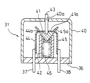
The pin-shaped leads 37 and 38 are mounted at fixed separated
positions from each other through an insulator base plate 36 of the thermal-
response switch 31. The leads 37 and 38 are made of conductive material,
e.g., for this example, the leads are made of iron-nickel alloy. The lead 37 is
connected to the communication line 11a, and the lead 38 is connected to the
communication line 11 b. A casing 40 covering the base plate 36 is attached to
the base plate 36. The casing 40 has a through-hole 40a located at a position
opposite from the base plate 36. A conic movable body 41 having a conductive
part 41a on an upper surface thereof is provided inside the casing 40, and is
held against the upper end of a glass tube fixed to the base plate 36. A reset
pin 43 is attached symmetrically to a central part of the upper surface of the
movable body 41. The reset pin 43 projects through the through-hole 40a, and
the movable body 41 is adapted to contact the glass tube 42 when the reset pin
43 is pushed.
Each lower end of a pair of thermal-response pieces 44 and 45 is
connected to the leads 37 and 38 inside the casing, respectively. For this
20724 1 9
example, each of the thermal-response pieces 44 and 45 is a bimetailic piece
that is a joined body of two metal pieces of manganese and Invar, wherein one
metal piece has a different thermal expansion coefficient from that of the othermetal piece. Each of the thermal-response pieces 44 and 45 is provided at
upper parts with narrow necks 44a and 45a, respectively, which hold the
movable body 41 attached to the glass tube 42, and which electrically connect
leads 37 and 38 through conductive part 41a. The thermal-response pieces 44
and 45 are transformed and expanded by heat at temperature of 100~C or more
to thereby release the movable body 41. A coil spring 46 is provided inside the
glass tube 42. When compressed, the spring 46 presses against the movable
body 41 held by pieces 44 and 45. Spring 46 pushes the conductive portion
41a of movable body 41 away from the thermal-response pieces 44 and 45
when the movable body 41 is released.
In the surge-absorbing circuit thus composed, when an overvoltage
and overcurrent are continuously applied to communication lines 11 a, 11 b, and
12, the thermal-response pieces 44 and 45 of the thermal-response switch 31
generate heat because they themselves are resistors. When the temperature
of the thermal-response pieces 44 and 45 rises to a predetermined temperature,
the thermal-response pieces 44 and 45 open. The movable body 41 is then
released due to the elastic force of the spring, which projects the reset pin 43through the through-hole 40a. The thermal-response switch 31 becomes
opened, thus stopping the continuous overvoltage or overcurrent from flowing
to the electronic device 10 and to the surge-absorbing element 14.
The reset pin 43 is then pressed after the temperature of the
thermal-response pieces 44 and 45 decreases below the predetermined
temperature for restoring those pieces to their original shape. Consequently,
the movable body 41 becomes supported firml-y by the thermal-response pieces
44 and 45 to thereby reconnect the electronic device 10 to the communication
lines 11 a,11 b, and 12. Contacting the conductive part 41 a of the movable body41 with the thermal-response pieces 44 and 45 is ensured by the elastic force
20724 1 9
. ,
of the spring 46, thereby resulting in a high-vibration-proof thermal-response
switch 31.
Operation conditions of the thermal-response switch 31 can be
easily checked by visually checking the extent to which the reset pin 43
5 protrudes from the through-hole 40a.
Example 2
Figure 3 shows another embodiment of this invention. In Figure
3, the same numerals as shown in Figure 1 illustrate the same parts as shown
in Figure 1.
A thermal-response switch 51 in this embodiment provides a third
lead 39 through the insulator base plate 36, in addition to the first and secondleads 37 and 38. A lower end of a coil spring 56 having conductivity and
thermal-respondency is connected to the lead 39. An upper end of the spring
56 presses on a movable body 41' of conductive material. The spring 56
extends so as to push away the movable body 41' from the thermal-response
pieces 44 and 45 during heating. The spring 56 is also composed so as to
electrically disconnect the leads 37 and 38 by lifting the movable body 41' off
the thermal-response pieces 44 and 45, and to simultaneously cause the reset
pin 43 to project through the through-hole 40a.
One or both of the leads 37 or 38 are connected to the
communication line 11 a, and the lead 39 is connected to the communication line
11 b, respectively. Repeated explanation is omitted because operations of this
surge-absorbing circuit are the same as those of the circuit in the above
Example.
In the surge-absorbing circuits of Examples 1 and 2, tests were
conducted in which an overvoltage or overcurrent was applied. The thermal-
response switches 31 and 51, and the surge-absorbing element 14, were
connected to the communication lines 11a, 11b and 12, and the electronic
device 10, respectively, as shown in Figure 2. A relatively small electric current
of an overvoltage, i.e. an electric current of 2.2 A at AC 600 volts, was passedthrough communication lines 11a and 12 of the test circuits for 30 minutes.
20724 1 q
As a result, in Example 1 the circuit was disconnected at about
three seconds after applying an overvoltage. Once the circuit was
disconnected, the circuit was not restored even after removing the over-voltage.However, the circuit could be restored by pushing the reset pin 43 into the
5 casing 40. Once in the restored condition, a vibration was applied by using a
stick having rubber around the pointed end; however, the circuit was not therebydisconnected. Example 2 gave the same result as Example 1.
, ~ !