Note: Descriptions are shown in the official language in which they were submitted.
Case 3335
2~72~17
MULTI-LAYER CIRCUIT BOARD
Field of the Invention
This invention relates to a multi-layer circuit
board and more particularly to a circuit board
having improved heat dissipation capabilities.
Backqround of Invention
Printed circuit boards having multiple layers,
each containing leads that may be interconnected to
each other between layers for joining various
semi-conductor components mounted upon the board
have become more popular. As the number of
components upon a board has increased while the size
of the board has decreased, it has become ever more
important to carefully plan interconnections of
leads between components. For larg~ logic arrays
having a great number of pin connections, it is
quite probable that leads will necessarily cross
each other. Clearly, if all leads were located on
the same power plane of the board, the circuit would
become shorted.
In the past, the problem of crossing leads in a
large two dimensional circuit board 20 having a
I hereby cortify that this correspondenco 18
being deposited with Ihe U.S. Postal Service
"Express Mail" Service on 7/2jl~
under Express Mail No. Q~ I *'lq~ ~ and is
addressed to the U.S Comrnissioner of Patents
and Trademarks, Washington, D.C. 20231.
Name:~,~;~
~ ~i
natur~ of Si~.
2~728~7
--2--
number of integrated circuit chips 21 thereon was
addressed in a manner shown in FIG. 1, i.e. by
breaking one of the two crossing leads 22 prior to
its junction with the other lead 24 and providing an
externally disposed jumper wire 26 that bridges the
crossed lead 24 without electrical contact
therebetween. However, as circuits have become
increasingly more complex, jumpers have become too
numerous and bulky, increasing the risk of failure.
Thus, concern for reliability has dictated that a
multi-layer "sandwich" approach, rather than jumper
wires, be employed. As such, the now popular
multi-layer boards generally provide a printed
circuit base layer upon an insulated (epoxy glass)
rigid board. The first (base) conductive printed
circuit layer includes leads and pads for mounting
various semi-conductor components. Leads that
otherwise cross, are left broken before their
potential crossing point and then a second layer of
insulation is disposed over the board at all points
except the very ends of the broken leads. A second
conductive layer is located at selective points to
bridge the unbroken leads between predetermined
junctions. Additional layers of insulator and
conductive material may be selectively applied, one
atop the other, until all junctions are bridged and
all connections between components are completed.
2~72~7
--3--
One advantage of the multi-layer system is its
ability to allow extremely close packing of
semi-conductor components onto a given surface of
circuit board. This fact, combined with the general
trend in the electronics design field to produce
higher power and larger heat generating components
(as much as 50 watts in the case of recen~ pin array
microprocessors) leads to an enormous generation of
heat that must be dissipated. Without effective
heat dissipation, the circuit would soon fail and
its components might even suffer mechanical failure
of their lead connections due to extreme
differential expansion of the various materials of
the component and board relative to each other.
Thus, as shown in FIG. 1, very high thermal output
components such as a power supply integrated circuit
chip 28 were in the past often isolated on a heat
sink circuit board 30 having a metallic or similar
heat dissipating base 32. The power supply chip 28
is, thus, interconneted to the main logic board 20
by wire leads 34.
Even in situations involving the use of lower
heat generating components, it is desirable to
incorporate power supply chips on the same board as
the complex logic and analog components. Since
power supplies, themselves, generate a large
quantity o~ heat, a board that adequately dissipates
2~72~7
heat must be provided for this multi-layer
application. The conventional epoxy glass and
fiber-type electrically insulating circuit board
cannot fulfill this requirement.
Summary of the Invention
It is therefore an object of the present
invention to provide a multi-layer circuit board
with high heat dissipating characteristics.
It is another object of this invention to
provide a multi-layer circuit board that allows the
incorporation of a power supply component with
multi-lead logic and analog components on the same
board.
It is another object of this invention to
provide a multi-layer circuit board that may be
constructed with relative ease in a variety of
configurations.
It is yet another object of this invention to
provide a multi-layer circuit board that enables
formation of a large number of connecting planes and
mounting of a large number of multi-connection
components upon a single relatively compact board
with reliable performance thereof.
A multi-layer heat dissipating circuit board
for mounting a plurality of heat generating circuit
chips thereon according to this invention provides a
207~17
base plate composed preferably of aluminum or other
highly thermally conductive material. The base
plate has disposed thereover a bottom insulating
layer that prevents electrical contact between the
base plate and any upwardly disposed layers of
circuitry. The insulating layer may be formed
preferably of a thermally conductive dielectric
epoxy. Positioned over this insulating layer are a
plurality of alternating layers of electrically
conductive strips and selectively disposed
intervening insulating layers such that
predetermined strips in each conducting layer are
separated from those in other conductive layers by
means of the insulation while predetermined
locations between conductive strips in different
layers are exposed to each other allowing electrical
contact therebetween. Some of the conductive strips
may be formed using a conductive ink such as silver
filled epoxy while insulating layers may be composed
of a dielectric thermally conductive epoxy. Both
insulating and conductive layers may be applied ~y
means of silk screening. A bottom-most layer of
conductive strips may comprise etched copper foil
that is applied to the bottom layer of insulation
using a thermally conductive adhesive. Similarly,
mounting pads for each of the circuit chips may be
formed in this copper foil layer.
2~728~7
--6
Brief DescriPtion of the Drawinqs
The foregoing objects and advantages will
become more clear with reference to the following
detailed description of a preferred embodiment and
drawings in which:
F~. 1 is a somewhat schematic perspective view
of a circuit board arrangement according to the
prior art;
FIG. 2 is a partially broken view of a
multi-layer heat dissipating circuit board according
to this invention;
FIG. 3 is a top view of the first conductive
layer of the circuit board of FIG. 2;
FIG. 4 is a cross-sectional side view along
line 4-4 of FIG. 3;
FJG. S is a top view of the second insulating
layer of the circuit board of FIG. 2;
FIG. 6 is a ~ross-sectional side view along
line 6-6 of the circuit board of FIG. 5:
FIG. 7 is a top view of the third conductive
layer of the circuit board of FIG. 2;
FIG. 8 is a cross-sectional side view along
line 8-8 of the circuit board of FIG. 7;
FIG. 9 is a top view of the circuit board of
FIG. 2 including circuit chips attached thereto;
FIG. 10 is a cross-sectional side view along
2~72~17
-7-
line 10-10 of the circuit board of FIG, 9; and
FIG. 11 is a cross-sectional side view along
line 11-11 of the circuit board of FIG. 9.
Detailed ~escriPtion of the Prefe,rred Embodiment
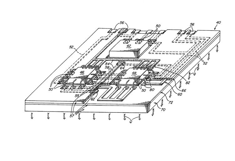
A multi-layered/multi-plane circuit board
having both power supply and logic integrated
circuits as illustrated in FIG. 2. The circuit
according to this embodiment is relatively simple in
comparison to the highly complex circuit designs
contemplated according to this invention, The
circuit board 40 specifically includes one power
supply chip 42 and two twelve-pin logic chips, Logic
I 46 and Logic II 48. The wire leads 50 of each of
the chips 42, 46, 48 are connected together
variously by means of conductive strips 52, 54 or
leads that carry electrical current between these
leads 50. External lead contacts 56 are further
provided upon an edge of the circuit board 40 for
connecting with exterior components via plugs,
solder joints and the li~e. The conductive strips
52, 54 are connected variously to these contacts 56.
In order to avoid the need for jumper wires 26
as depicted in FIG. 1, the circuit board 40 is
formed in a plurality of planes 57 of alternating
insulating and conducting materials. The particular
materials utilized and their method application will
207~17
--8
be discussed further below, but generally, multiple
layers o strips are employed in locations upon a
circuit board where a conductive strip must cross
one or more conductive strips on the same plane
without the crossing strips coming into contact, as,
for example, in the bridge 55 of FIG. 2. In this
embodiment, one set of parallel conductive strips 58
is positioned upon a lower layer 60. The bridging
strip 55 must cross this set. Therefore, bridging
points 62, 64 aside the set of strips 58 are
established upon the lower layer 60 for the crossing
the set of strips. An upper layer of insulation 66
is, thus, applied over the lower layer 60 of
conductive strips except for the region proximate
each of the bridging points 62, 64 which remain
exposed.
A column of conductive material fills the gaps
in the insulation over each of the bridging points
to bring the conductive material level at these
points up to the level of the surface of the
insulating layer 66. The bridging strip 55 on the
surface of the insulating layer 66 is formed between
the two filled bridging points 62, 64. The bridging
strip 55 is thus, physically and eleotrically
separated from the lower set of crossed strips 58 by
means of the intervening insulating layer 66.
The multi-layer circuit board 40, according to
2072~7
this embodiment, is designed for closely fit
mounting of a plurality of integrated circuit chips
and components thereon. In particular, the board 40
may accommodate, in combination with the logic chips
46, 48, a power supply chip 42. As such, a
significant quantity of heat is generated during
normal operation of the board's circuit components.
Thus, the multi-plane board of this invention
includes a base plate 70 comprising metallic or
other highly thermally conductive material. Other
types of materials haing high thermal conductivity
include ceramic substrates, pure metals and
polymeric systems such as polyimides. In this
embodiment, an aluminum alloy plate of approximately
1~16" thickness is utilized. The plate 70 should
generally remain uncovered upon a face opposite the
circuitry so that heat Q may be freely dissipated to
the environment by means of air convection and
radiation. Note that corrugation or other texturing
may be placed upon this surface to further increase
conductivity. The base plate side proximate the
circuitry should, conversely, be covered with a
bottom layer 72 of dielectric insulating material.
Since the plate 70 of this embodiment is metallic
and electrically conductive, the layer 72 should be
sufficiently thick to isolate any upwardly disposed
circuitry from the metallic surface of the base
2072~17
--10--
plate 70. A suitable dielectric layer may be
obtained by applying a one or two component
dielectric thick film epoxy such as ME 933-53 or ME
51-46, respectively, by the Emerson & Cumming, Inc.
Alternatively, an insulating layer may be formed
using a polyimide, urethane, silicone or polyester
compound among others. A layer of from 3 to 10 mils
should suffice in most circumstances to prevent
electrical contact of the base with upper layers.
It is important that the epoxy utilized possess
sufficien~ thermal conductivity to assure adequate
transmission of generated heat from the upper
circuit layers to the base plate. Otherwise, excess
heat retained by the upper layers may cause damage
to the circuit leads and semi-conductor components.
Above the insulating epoxy bottom layer is
deposited an initial conducting layer 60. The
deposition of this layer is shown, particularly, in
FIGS. 3-4. Note that printing or silk screening is
the preferred method of deposition in this
embodiment. It may be used for the leads and
insulator and even for certain components such as
resistors. A variety of conductive materials may be
utilized for the first layer. However, general
practice has developed a preference for a solid
copper foil layer that is adhered to the insulating
material using, for example, an aluminum oxide based
thermally conductive epoxy in a 3 mil layer. The
copper foil is subse~uently masked to form a lead
2~2~7
pattern. The board surface is then exposed to acid
that dissolves unmasked copper such that the board
is selectively e~ched to remove all copper material
except the desired lead pattern. Such a lead
pattern is particularly illustrated in FIG. 3 and
corresponds to the lower layer conductive strips 52
(shown in phantom) of FIG. 2.
The conductive lead pattern includes pads 74,
76 and 78 respectively, for mounting the power
supply 42 and each of the logic chips 46, 48. The
pads 74, 76, 78 of copper foil in this embodiment
provide excellent heat sink qualities for directing
thermal energy from the chip to the base plate with
a minimum dispersion within the upper board layers
and they also facilitate firm mounting of the chips
to the board. Chips may, in particular, be mounted
by means of solder or adhesives in a manner
described further below.
Around each chip mounting pad 74, 76, 78 are
positioned a plurality of contact pads 80 for
interconnection of chip wire leads to the desired
conductive strips. As discussed above, the layout
of conductive strips also includes a pair of
bridging points 62, 64 that take the form of contact
pads, in this embodiment. The electrical circuit
connection between bridging points 62, 64 is, of
course, broken on the lower conductive layer 60 of
'
- 2~72~7
-12-
FIG. 3.
After forming the lower layer 60 of conductive
I strips, it is subsequently covered, in select
locations, with an upper layer 66 of insulating
dielectric thermally conductive epoxy as depicted in
FIGS. 5-6. The object of the application of the
upper insulating layer 66 is to cover all parts of
the lower conductive layer 60 except the connection
poin~s that are to be accessed by subsequently
applied upper disposed conductive layers and
component leads. Each mounting pad 74, 76, 78 is
also left uncovered since it is desirable to place
the heat generating chips as close as possible to
the base plate. Additionally, each lead contact pad
80 on this layer generally remains uncovered so that
a corresponding chip lead wire may be attached
thereto. Bridging points 62, 64 are also left
uncovered to be electrically connected in the next
conductive layer.
The application of the upper insulating layer
66, according to this embodiment, may be performed
via a variety of methods. Silk screening of the
epoxy inæulating material over selected areas of
lower layer strips 52 provides a highly accurate and
precise application method of alternatively covering
and exposing sections of leads according to this
embodiment. Alternatively, vapor deposition
2072~:~7
-13-
(sputtering) or electro deposition, in the case o
conductive strips, or other suitable coating methods
may be utilized.
Following deposition of the upper insulating
layer 66 to selected locations of the lower
conductive layer 60, an upper conductive layer 82 of
leads or strips 54 is then deposited thereover.
While it is possible to apply the second conductive
layer 82 using solid copper sheet or foil in
combination with masking of exposed contact points
from the first layer and then etching the shee~ to
obtain the appropriate strip configuration, it is
not generally practical to do so. Rather, a polymer
base thick film conductive compound, including
various forms of conductive "ink", such as Emerson &
Cumming, Inc. silver-filled epoxy C 933-34 is
utilized to lay down strips 54 at selected
locations. An epoxy of such type, is then hardened
using elevated temperature curing to develop optimal
properties.
The conductive epoxy leads 54 of the upper
conductive layer 82 may be disposed wholly upon the
surface of the upper insulating layer 66, or may
partially impinge upon and contact the lower
conductive layer 60 through exposed locations in the
insulation 66 therebetween. Such contact occurs,
for example, at the two bridging points 62, 64.
207~7
Since the conductive compound or in~ is a polymer
thick film (as opposed to an inorganic such as
alumina), it tends to flow into crevices and fill
them. As such, the ink may be built up to fill the
columns around exposed points of the lower
conductive layer 60, thus, bringing the upper
conductive layer 82 up to a level that is even with
or above the level of the upper insulating layer
66. Alternatively, solder or similar gap filling
conductive compositions may be utilized in a
separate application step to build a conductive
column between layers. Since the insulating layers
between conductive layers are only a few mils thick,
minimal gap filling is necessary at exposed points
which facilitates silk screening techniques.
While silk screening is relatively precise in
its deposition of materîal, closely spaced lines of
conductive epoxy may still necessitate masking of
contacts in lower layers. One such point where
masking may be required is the bridging point 64
(FIG. 8), to prevent its inadvertent connection with
the adjoining strip 86 of conductive epoxy during
application of additional conductive material. ~uch
masking could be removed by an appropriate solvent
following the deposition of the conductive layer to
reexpose these leads for further connections.
While the above-described embodiment shows only
2072317
-15-
two alternating layers o conductive strips with a
layer of insulation therebetween, the steps
described in FIGS. 3-8 may ~e repeated by
selectively depositing additional layers of
insulation and conductive strip material, one over
the other, until rather large lattices of
interconnected layered strips are created. Columns
for connecting one layer to another, or several
layers together, with connected layers in both
adjacent and non-adjacent positions relative to each
other, may be formed at any location upon the
surface of a circuit board. Connectior.s of such
type are performed by leaving a contact point of a
lower layer exposed while building up successive
layers that continue to expose the contact point and
then finally forming a conductive column to an upper
lead from the contact point through the open "hole"
in the layers therebetween. Note that a final
insulating layer may then be applied over all the
layers so that only the remaining desired contact
points are exposed. One may even apply an upper
ground plane to the top layer of the board.
~ FIG. 9 illustrates the final attachment of the
- circuit chips 42, 46, 48 to the board with wire
leads 50 attached to the exposed contact points of
the two-conductive layer circuit board embodiment of
FIG. 2. While an insulating layer, as discussed
- 2~72~17
-16-
above, may be applied to the upper conductive
strips, leaving only the strip colltact pads, and
edge plug contact points 55 exposed, such a layer
has been omitted in this example for added clarity.
Each chip wire lead 50 is attached by means of
solder or a similar electrically conductive adhesive
to its respective mounting pad 74, 76, 78. Since
the mounting pads have remained exposed, the chips
42, 46, 48 transmit heat almost directly to the base
plate 70. The wire leads 50 of the chips are then
attached to each respective contact pad 80 (FIG. 7)
by means of an electrically conductive adhesive or
solder. Note that the chip wire leads 90, 92 may be
attached to contact pads 94 and 96 respectively on
strips of differing conductive layers 60 and 82
respectively. For example, FIG. 11 illustrates a
left lead 90 attached through a hole 98 in the upper
layer of insulation 66 to lower layer conductive
strip 100 while a right lead 92 is attached to an
upper conductive layer strip 102. Again, further
upperwardly disposed layers of insulation and
conductive strips may be applied over the
illustrated layers according to this invention and
upper disposed leads may be positioned variously
through a given number of layers to electrically
connect to the appropriate lower strip.
It should be understood that the preceding is
2~72~7
-17-
merely a detailed description of a preferred
embodiment. It should be apparent to those skilled
in the art that various modifications and
equivalents may be made without departing from the
spirit or scope of the invention. The preceding
description is meant to be taken only by way of
example and to describe only a preferred embodiment
and not to otherwise limit the scope of the
invention.
What is claimed is: