Note: Descriptions are shown in the official language in which they were submitted.
2072830
.", .
This is a divisional application of Canadian Patent
Application 2,032,301 filed December 14, 1990.
This invention concerns a method and a system of
smoothing and control of asynchronous time communication
outputs by virtual circuits.
Systems of control of the flows of p~ckets or of cells
carried by asynchronous time multiplexes are already known.
The forwarding of any outputs and the divisions of the same
resources of transmission constitute the interest of
asynchronous time technology. It will be recalled that an
asynchronous time multiplex has the structure of that which
is described in the document EP-A-108028. In such a
multiplex, the data are transmitted by p~ckets of the same
length each preceded by a label of fixed length identifying
the virtual circuit to which the p~cket belongs. In the
following in order to conform with the designation now usual,
there will be designated by "cell" the label followed by the
packet. The asynchronous time multiplexing permits in
particular of transmitting in a same support, that is to say,
the asynchronous time multiplex, cells belonging to different
virtual circuits. The ~Ximum number of virtual circuits on
a multiplex is determined by the length in bits of a part of
the label which identifies each virtual circuit.
The allocation of the time multiplexes depends generally
on statistics of the rates of activity of the different
sources capable of having access there with the result that
there is a non nil risk of losses of information by
overflowing of the queues due to instantaneous overloads.
These losses must of course be ~ini~ized but the solution is
not easy because the flows supplied by the different sources
are of discontinuous character and are sporadic.
Furthermore, malevolent terminals are capable of injecting
into the network cells with a higher output than that which
has been allotted to them at the time of the establishing of
their communication.
The documents EP-A-293314 and EP-A-293315 already
describe each of the methods and systems of control of flow
2 2072830
,~
of packets in particular those which are carried by
asynchronous time multiplexes. The documents US-A-4475192
and US-A-46111322 likewise deal with traffic controls. On
this subject one can also refer to the article heA~e~ 'IThe
Challenge of Multiprint Communications by Jonathan S.
Turner, 5th ITC Seminar, Lake Como, Nay 1987, chapter 5 -
Congestion Control. This document defines in particular the
device known under the English name "leaky bucket".
Generally speaking in these flow controls the excess cells
are eliminated when the number of cells received exceed the
quantity provided for at the time of establishing the
communication~ this number being evaluated on a time
corresponding to the dispension of maximum admissible
propagation time. This dispension of propagation time is
currently evaluated for a very low associated rate of loss,
in the order of 10-1~.
These known methods, systems and devices satisfy well
the conditions of clipping of output but if there is a burst
of consecutive or almost consecutive cells belonging to a
same virtual circuit, even if the number of cells does not
exceed in the burst the number authorised during the
measuring interval considered, the burst risks creating an
instantaneOus overload in the lower part of the time
communication network. In fact, the duration of the bursts
assi~;lAble by the network is clearly below the amplitude of
the dispension of propagation time expected. It should be
noted that these bursts or "lumps" of cells may be produced,
not only by the sources but also by the upper multiplexing of
asynchronous time flows.
One object of the present invention consists in
providing a method and a system which not only realises a
control of the traffic by eliminating the excess cells but
also by smoothing the above-mentioned bursts.
3 ~
In accordance with an embodiment of the
invention, a method of controlling the flow of cells in
an asynchronous time-division communication system by
s forming cells received from an in-coming asynchronous
time-division multiplex system (XE) into cells delivered
to an out-going asynchronous time-division multiplex
system (XS), the method comprises the steps of storing
each received in-coming cell in a buffer memory (MT) and
at an address (Add) that corresponds to a real time (t)
for re-sending the stored cell over an out-going time-
division multiplex system (XS); comparing a first number
of cells (N) of a particular communication which are
already stored in the buffer memory (MT) and that have
not been resent at the time when the next cells relating
to the particular communication arrive with a maximal
number (NM) which is assigned to the particular
communication; and denying a re-sending of the next in-
coming cell if the comparison finds that the first
number exceeds the maximal number.
In accordance with another embodiment, the
method described above further comprises a status memory
(MCO) and an arithmetic and logic unit (UAL), the status
memory (MCO) being divided into a plurality of zones,
each zone bi-univocally corresponding to a communication
received over in-coming asynchronous time-division
multiplex (XE) and comprising two sections (N and NM);
the further steps comprising storing in a first section
(N) a number indicating the number of cells of the
communication that are stored in the buffer memory (MT)
and that have not yet been sent at the time of arrival
of the next in-coming cell of the same communication;
storing in a second section (NM) the maximal number
assigned to the communication; using the arithmetic and
logic unit (UAL) for making the comparison between the
first number (N) and the second number (NM); and
inhibiting the re-sending of the in-coming cell, when
the first number (N) exceeds the second number (NM).
~,~
' ~072830
X The abovementioned characteristics of the invention will
appear more clearly on reading the following description of
one embodiment, the said description being made in realtion
to the attached drawings among which:
Fig. 1 is a block diagram of a system according to the
invention;
Fig. 2 shows structures of words corresponding to hours
or intervals of time used in the system of Fig. l;
Fig. 3 is a block diagram of an arithmetical and logical
unit used in the system of Fig. l;
Fig. 4 is a diagram of the arithmetical part of the unit
of Fig. 3;
Fig. 5 shows time organigrams illustrating a case of
operation of the system by the invention;
Fig. 6 shows also time organigrams illustrating another
~case of operation; and
Figs. 7 to 9 show the tables of the logical divisions
taken in the logical part of the unit of Fig. 1.
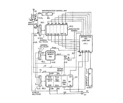
The system of Fig. 1 comprises an input queue FiFo, a
slate memory MCO associated with an arithmetical and logical
unit UAL and with an address multiplexer MIX 1, a memory of
addresses available MAD associated with an address
multiplexer MX2, a buffer memory MT associated with an
address multiplexer MX3, gates AND Pl and P2, a time base BT
and microprocessor control unit UC.
To the input of the queue memory FiFo is applied the
incoming multiplex XE. The gate P1 supplies the leaving
2072830
._
multiplex XS.
In the embodiment described, the multiplex XE is an
asynchronous time multiplex of the type which is described in
the document EP-A-108028 but the p~ckets of which, now called
"cells are assumed to have been put in parallel form with
424 bits. This size of 424 bits corresponds to that of a
cell which has been adopted in June 1989 by CClTT. The
memory FiFo is an alignment queue similar to that which is
described in the document EP-A-113307 the role of which is to
adapt the incoming input to the local clock t of the system
of Fig. 1. Each cell leaving the queue FiFo is therefore
synchronous with the local clock and i~ presented on a bundle
Fe of 424 wires the first sixteen EQe of which transmit the
first sixteen bits which constitute the label Vcie which
identifies the virtual circuit which conveys the cell, that
is to say, which identifies the communication concerned.
The queue FiFo has also an output PP which carries a signal
of the same name which indicates whether the interval of time
entering is free or engaged. The signal PP is obt~i ne~ as
shown in Fig. 1 of the document EP-A-113307. The result is
a bundle of 425 wires leaving the memory FiFo. The 425th
wire carrying the signal PP and being connected to the input
of the same name of the circuit UAL.
The state memory MCO is a live memory with aleatory
access comprising as many zones as communications which the
system can deal with. Each zone is divided into six
sections respectively inten~PA to memorise:
- the theoretical time of emission of the last arrived cell
tde,
- the minimnm theoretical period pm,
- the theoretical time of emission of the last emitted cell
tdl,
- ~inimum delay dm,
- the number NM, and
- the number N.
6 20 72830
The memory MCO has six inputs al to a6, corresponding
respectively to the six sections mentioned above. It
comprises likewise six outputs bearing respectively the same
designations as the sections. Finally, its address input is
connected to the output of the multiplexes with three inputs
MXl .
The first input of the multiplexer MXl is connected to
the bundle EQe bearing the label Vcie of the incoming cell,
its second input is connected to the bundle EQs bearing the
label VCis of the outgoing cell and its third input UCa is
connected to a corresponding output of the control unit UC.
The control input of the multiplexer MXl is connected to the
outputs E, S and U of the time base BT.
The time base BT supplies the local time t each
elementary time of which corresponds to the reception of an
incoming cell and to the emission of an outgoing cell. As
Fig. 2 shows, the hour t serving to follow the chronology of
the events is given on twenty-four bits a first part of heavy
weight of which is composed of eight bits followed by a
second part of lighter weight of sixteen bits. As will be
seen later, the first part permits of marking the long-term
events and the second serves for the addressing of the memory
MT and therefore marking the events in each operating cycle
of the memory MT.
The time tde defined above is given on thirty-two bits a
first part of eight bits of which and a second of sixteen
bits, as for t, plus a third part of eight bits of
lightweight constituting a decimal part the role o~ which
will be seen later. In normal operation, the time tse is
deduced from the theoretical time of emission of the
proce~i ng cell of the same communication by A~ i ng to it the
value Pm which represents the theoretical minimum period of
re-emission of the cells of the communication concerned.
The hour tde is so-called theoretical because the actual time
of emission of the cells concerned may differ therefrom given
2072830
the possible conflicts between the theoretical times of
emission of cells belonging to different communications.
The period E_ is given on twenty-four bits the part of
sixteen bits of which serving indirectly for the addres~ing
of the memory MT and the decimal part of eight bits. The
period Pm corresponds to the minimum time which must
theoretically separate the re-emission times of two
consecutive cells in order to avoid the effect of ~specks"
and consequently to smooth the output of the cells.
The decimal part permits of selecting any output which
is not necessarily a submultiple of the output of the
outgoing multiplex XS.
The theoretical time of emission of the last cell
emitted tdl is coded on thirty-two bits, as tde, corresponds
to the theoretical time at which the last cell of the
communication concerned would have to be emitted even if its
actual tLme of emission has been a little later.
The m~xi~ll~ delay dm is coded on twenty-four bits, as E~
and corresponds to the maximum delay time admissible which a
cell in the network can take, taking into account the
dispension of propagation time admitted which has been
mentioned in the preamble. In order to take into account
this dispersion, smoothing the outputs up to this time valve
dm is accepted. If, in consequence of consecutive bursts of
cells in the same communication one cannot guarantee this
delay, the cell concerned is destroyed. The delay dm may
vary as a function of possible priorities between different
communication cells.
The time base BT supplies in addition to the local time
t and for each elementary time, six successive signals tl to
t6 which occupy together an elementary time. The times tl
and t2 are used for the corresponding treatment on the
arrival of an incoming cell, the times t3 and t4 for the
corresponding treatment on the emission of an outgoing cell
and the times tS and t6 for the treatment of the access to
2072830
the memory MCO by the control unit UC. Further~re, the
output tl and t2 are ~oined to supply the signal E, the
outputs t3 and t4 to give the signal S and the outputs t5 and
t6 to give the signal U. The signals E, S and U serve in
particular to control the multiplexes MXl to MX3.
The reading of the memories is effected at tl, t3 and tS
whilst the rewriting, after calculations, is effected at t2,
t4 and t6.
The buffer memory MT is a live memory with aleatory
access comprising spaces the number of which will be defined
in the following. Each space is divided into four sections
respectively intended to memorize:
- the field of useful data DON of a cell,
- the label Vcie of the corresponding cell,
- the theoretical hour of emission tde of this cell, and
- a bit b5 which when it is at "1" indicates that the
space addressed in reading contains a useful cell to
transmit.
The memory MT has four inputs corresponding respectively
to the data DON, the label Vcie, the theoretical time of
emission hte and the bit be. It comprises likewise four
outputs bearing respectively the references DON, Vcis, tdse
and bes. The outputs DON and Vcis are regrouped in a bundle
of 424 wires connected respectively to the first inputs of
424 gates AND Pl the second inputs of which are connected to
the output bes. The addressing input of the memory MT is
connected to the output of the multiplexer MX3.
The first input of the multiplexer MX3 is connected to
the output of the memory MAD and its second input receives
the current time t of the time base BT. Its control input
is connected to the outputs E and S of the base time BT.
The memory MAD iS a live memory with aleatory access
comprising as many spaces as the memory MT, each space having
a capacity of one bit and corresponding biunivocally to one
space of the memory MT. It has an input dispo which is set
9 2072830
..--
at "1" or at "0" according to whether the memory MT is in
writing or reading mode. It has an output Add. It
comprises two address inputs Adrl and Adr2. The input Adrl
is connected to the output of the multiplexer MX2 one input
of which is connected to the output Add of the memory MAD and
the second output of which receives the local time t of the
time base BT. The control input of the multiplexer NX2 has
its control input connected to the outputs E and S of the
time base BT. The control input of the multiplexer MX2 has
its control input connected to the outputs E and S of the
time base BT. The address input Adr2 is connected to the
output of the gate P2.
The output Add of the memory MAD is connected to the
first input of the multiplexer MX3.
In the memory NAD, one space contains an 'O" to indicate
that it is free and a "1" to indicate that is is engaged.
The memory MAD supplies permanently to its output Add the
address of a free space, this address being previously
selected from the binary value of a field of sixteen bits
extracted from the theoretical time of emission hte of the
cell considered, that is to say, from the signal al which
will be described later and which is applied to the first
input of the gates P2. The second inputs of these gates P2
are connected to the output E of the time base BT which
signifies that the input Adr2 of the memory MAD is only
active during the treatment of an incoming cell and precisely
to find an address Add of free space in the memory MT. A
memory such as memory MAD is described in the document FR-A-
2617602 with the title "Circuit for memorising state of
availability of logical sources, such as memory cells and for
establishing addresses of free resources". In practice the
memory MAD comprises means for sc~nning the space which is
designated by hte and when the space is not free, the
following spaces and for stopping the sc~nning at the first
free cell the address of which is then supplied by Add.
2072830
. ....
The arithmetical and logical unit UAL associated with
the memory MC0 is represented in the block diagram of Fig. 3.
It comprises an arithmetical part UAR and a logical decision
part UDL. The part UDR, Fig. 4, comprises four adders ADDl
to ADD4, a proximity to zero test circuit TV2, five OR-
inclusive gates P3 to P7 and five comparators COMl to COM5.
The circuit UAR comprises the inputs tde, tdl, dm, E, L,
N, NM, t and ~_. It comprises likewise the outputs.t-pm, N-
+1, tse, bl, b2, b3, cl, dl, el, fl and f2.
The circuit ADDl is an arithmetical adder which has its
two inputs connected respectively to the input tde and ~ and
its output to the output tse which supplies the time (tdm +
pm).
The circuit ADD2 is an arithmetical adder which has
three inputs, one of which is connected to the input tdl, the
second to the input dm and the third receives per~nently the
value CMT which corresponds to the number of spaces in the
memory MT. By way of example, the value may be 216, that is
65536. The exponent 16 corresponds to the sixteen bits of
the second part of t, Fig. 2. The eight bits of heavyweight
t permit of not having zero value at each cycle of the buffer
memory MT but a passage through zero only every 224
elementary times of the time base BT which corresponds to a
period T of the latter.
The output P of the adder ADD2 which supplies the value
(tdl+dm+216) is connected indirectly through the gate P5 for
its heavy weight bit, to the second input Pc of the
comparator COM4.
The circuit ADD3 is an algebric adder which has two
control inputs respectively connected to the inputs E and L
and two inputs one of which is connected to the input N and
the other receives permanently the value ~'1". Thus, when
the input E is activated, the circuit ADD3 adds "1" to the
value N whilst when the input L is activated, it subtracts
"1" from the value N. Thus, the output of the ADD3 supplies
11 2072830
either (N+l) or (N-1) and is connected to the output N-+I and
to the first input of the comparator CDM3.
The circuit ADD4 is an arithmetical subtractor which has
its two inputs connected respectively to the inputs t and pm.
Its output supplies the value (t-pm) and is connected to the
output t-pm.
The circuit TVZ has three inputs zl to z3 and one output
Y. The inputs zl to z3 are respectively connected to the
heavy weight bit wires of the input tdl, the output P of the
adder ADD2 and the input t, these wires likewise being
respectively connected to the first inputs of the gates P4 to
P6. The output Y is at "1" when, among the three heavy
weight bits applied to its inputs, the binary value of one of
them differs from those of the two others. The output Y is
connected to the second inputs of the gates P4 to P6.
Furthermore, the heavy weight bit wire of the input tde is
connected to the first input of the gate P3 the second input
of which is connected to the output Y of the circuit TVZ.
Finally, the heavy weight bit wire of the output tse is
connected to the first input of the gate P7 the second input
of which is also connected to the output Y.
In the case where Y = O, the heavy weight bit of each of
the values tde, tse, tdl, P and t is not changed in passing
with its associated OR-exclusive gate. In the case where Y
= 1, the heavy weight bit changes value at the output of the
gate P3 to P7 which leads, once it has been associated with
the rest of the lightweight bits to have all the values in a
zone not comprising the value zero of a complete cycle of the
time base BT and therefore being able to compare them without
ambiguity in the comparators COMl, COM2, COM4 and COM5 around
the value T/2.
The comparator COMl has its two inputs tdlc and tdec
respectively connected to the outputs of the gates P4 and P3.
If output bl is activated when tdec is higher than tdlc, the
output b2 is activated when tdle is equal to tdlc and the
12 2072830
output b3 is activated when tdec is lower than tdlc.
The comparator COM2 has in input tc connected to the
output of the gate P6 and an input tdlc connected to the
output of the gate P4. Its output cl is activated when tc
is lower than tdlc and its output c2 when tc is equal to or
higher than tdlc.
The comparator COM3 has its first input which receives
N-+l and its second input connected to the input NM. Its
output dl is activated when N-+l is higher than NM.
The comparator COM4 has an input tc connected to the
output of the gate P6 for the heavy weight bit and to the
input t for the light weight bits and an input Pc connected
to the output of the gate P5 for the heavy weight bit and the
output P for the rest of the light weight bits. Its output
cl is activated when tc is higher than Pc and its output e2
is activated when tc is equal to or lower than Pc.
The comparator COMS has an input tc connected in
parallel on the input tc of the comparator COM4 and an input
tsec connected to the output of the gate P7 for the heavy
weight wire and to the output of the adder ADD1 for the rest
of the lightweight bits. Its output fl is activated when tc
is lower than tsec which is a normal case of a first type
whilst its output F2 is activated when tc is higher than tsec
which is a normal case of a second type.
The output signal tse produced by the adder ADDl
correspondS to a time which is the sum of the theoretical
time of emission of the preceding cell tde and of the minimum
period ~_. Fig. 2 shows that the time tse (tdepm) is, like
tde coded on thirty-two bits one part of which is decimal.
The signal t-Pm produced by the subtractor ADD4 corresponds
to a time which precedes the current time t of a value equal
to the mini~um period pm. The time is also coded on thirty-
two bits one part of which is decimal. It is used in the case
of reinitialisation, as will be seen in the following in
relation to Fig. 7. The signals NN and N-+1 are coded on
13 2072830
.~i,
twenty-four bits without decimal part. The signal NM
corresponds to a number which represents, for a
communicationr the m~Yi~ number of waiting cells in the
memory MT. The signal N-+1 is likewise a number which is
compared with the number NM in the comparator COM3. The
signal P produced by the adder ADD2 corresponds to a time
which is the sum of the time tdl, that is to say, the
theoretical time of emission of the last cell emitted plus
the maxi~ll~ delay dm between two cells, plus the number of
spaces of the memory MT. It is therefore certain that at
the hour P all the cells waiting in the memory MT have been
emitted, hence the interest of the compression of the current
time t with the time P as will be seen further.
The signal bl of the comparator COMl is at "1" when tdec
is higher than tdlc which expresses that on arrival of the
cell forming part of a correspondence, the theoretical time
of emission of the cell which has arrived just before is
later than the theoretical time at which the last cell of the
same communication has been emitted. It is a matter of a
normal case. The signal b2 at "1" corresponds also to a
normal case, that in which the two theoretical times are
equal. On the other hand, the signal b3 at "1~' expresses a
faulty case. It is not possible for the theoretical time of
emission of a cell belonging to a conversation to precede the
theoretical time of a cell of the same conversation already
emitted.
The signal cl produced by the comparator COM2 at "1"
expresses that tc is lower than tdlc. It is a question of a
faulty case since tdlc corresponds to the time te at a cell
already emitted. The output signal c2 at "1" corresponds to
a normal case.
The output signal dl of the comparator COM3 at "1"
corresponds to the case where the memory would accept a
number of cells of a conversation higher than that which has
been agreed at the beginning of the conversation, the number
14 207283~
~.
agreed being NM. It is therefore also a faulty case.
The output signal el of the comparator COM4 at "1"
expresses that te is higher than Pc. The signal c2 at "1"
corresponds to a normal case.
The output signal fl of the comparator at "1" expresses
that tc is lower or equal to tsec which corresponds to a
normal case of a first type as will be seen in the following.
The output signal f2 at "1" expresses that tc is higher than
tsec which corresponds to a normal case of a second type.
The signal fl and f2 of the comparator COM5 corresponds
to two types of normal cases as will be seen later.
Before considering in detail how the logical decisions
circuit UDL deals with the different cases as a function of
the signals bl to e2 which are applied to it we will
illustrate in relation to Figs. 5 and 6 two cases of current
and normal operations, the value Pm being four elementary
times.
In the time diagrams of Fig. 5:
- the line t) shows partially the unfolding of the local
time t that is, here the elementary times tl9 to t41,
- the line i) indicates the incoming cells of the
conversation i, that is, here il to i6 it being assumed
that it is not a matter of a beginning of conversation,
- the line tde) shows different values tde entered
successively in the zone corresponding to the
conversation 1 of the memory MCO,
- the line tse) indicates the different values of tse at
the corresponding output of the circuit UAR,
- the line hte) indicates the successive values of hte,
- the line Adr2) indicates the different initial addresses
applied to the memory MAD in order that it may search
for the address of an available following space in the
memory NIT,
- line add) indicates the addresses of the memory MT
successively determined by the memory MAD, by noting
~ 207~830
~,
that each value htc is also recorded at the same address
of MT, although this value may be different from this
address,
- the line tdlc) indicates the successive values of tdle
at each reading of the cell, the value of tdle being
called to be memorized in the form of tdl in the zone
corresponding to the conversation i in the memory, after
treatment in the logical decisions circuit UDL.
- the line tdl) indicates precisely the successive values
of tdl,
- the line N) indicates the successive numbers of cells of
the conversation i which are in the memory MIT and
- the line i') indicates the output times of the cells of
the conversation i, that is, here i'l to i'5
corresponding to il to i5.
In the time diagrams of Fig. 6 the same classes have
been adopted.
In the case of Fig. 5, the cells il to i5 arrive at the
input of the system of the invention by respecting the period
E_ of four elementary times except for i4 which arrives with
a time delay. The search for a free address in the memory
MAD is immediate except for the memorization of the cell 12.
Consequently the cells i'l to i'5 leave shortly after spaced
as the cells il to i5 are arriving. It will be remembered
that the period ~_ is the minimum theoretical period of
spacing between two re-emitted cells. In the case of Fig. S
it is assumed that the entering cells respect practically
this same period E~ and it is found that normally the re-
emitted cells also respect it.
In the case illustrated in Fig. 6, from the cell i2, the
min;~ll~ period ~_ is no longer respected, the entering cells
i3 to i5 arrive very close together but that then the
following cells arrives clearly later. It will be noted
however that the outgoing cells il to i4 are well spaced
which confirms that the system of the invention effects a
16 2 0 72 830
smoothing. Fig. 6 likewi5e shows that the number N may be
increased rapidly in case of bursts. If the burst i3 to iS
had continued, the number N would have been able to exceed a
maximum NM which would have entailed the elimination of the
last cells of the burst.
The two cases illustrated in Figs. S and 6 only
constitute examples of normal cases which permit of
deter~ining the faulty cases or other normal cases which will
now be described in detail considering Figs. 7 to 9.
As ~ig. 3 shows, the inputs of the logical decisions
circuit are: N-+l, t-pm, tse, bl, b3, cl, c2, dl, el, e2,
fl, f2, AM, bs, PP, tdle, t and tl to t6. There will now be
described successively the treatments carried out on the
arrival of an incoming cell, at the emission of an outgoing
cell and at the access of the central unit.
On the arrival of an incoming cell, this latter is
treated at tl, then t2, Fig. 7. The zone of the memory MCO
which corresponds to the communication i to which the
incoming cell belongs, is addressed through the multiplexer
MXl commutated by the input E = tl+t2, by the label Veie of
the cell. The state of the said zone of the memory MCO is
read at tl and its output signals applied to the circuit UAR
which supplies the signals bl to f2.
The different spaces indicated in the table of Fig. 7
represent the actions to be undertaken as a function of the
events defined by the signals bl to f2 (first line),
associated with the conditions entered in the second line.
The following cases will therefore be met:
1) b3 is at "1" whatever may be the other signals b2 to c2.
Normally the time tde is always higher or equal to the
time tdl ~ince tdl corresponds to an emitted cell and
tde to this same cell or to a following cell. It is
therefore a faulty case. However, according to the
system of the invention, the decision is taken to take
into account the incoming cell. At t2, the signals al
2072830
,~_
to a6 take the following values: t, that is to say, the
current time, x, t-pm, x, x, 1, x, indicating that the
value already existing in the corresponding zone of MCO
is unchanged. It will be seen in particular that at
the time tdl the value t-pm is allocated in order that
tdl may be different from tdc, which is useful for
following cases and that the number N takes the value 1
to indicate that there is a cell of the communication i
which has been memorised.
Furthermore, the sixteen bits of the signal al
corresponding to the sixteen lightweight bits of t are
applied by the gate P2 opened by the signal E to the
input Adr2 of the memory NAD which goes to search for
the address equal to or higher than t of a free space in
the memory NT. The bundle of 32 wires of al, always
through the gate P2 is extended towards the input hte of
the memory MT. The wire be is at "1". The memory NT
addressed by the multiplexes MX3 memorises the incoming
cell, the time hte and the bit be in the corresponding
space.
Finally, the memory MAD enters the bit "1" present at
the input disPo connected to the wire be in the address
space Add, the writing address being transmitted by the
multiplexes NX2 controlled by E.
2) cl is at "1" whatever may be the signals el, b2, dl, c2
and e2.
This case cannot normally be produced and it is
therefore a faulty case. It is decided to take the
incoming cell into account and the same actions as at 1)
above are taken.
3) el and b2 are at "1" whatever may be the signals dl, b2,
c2 and e2.
This case signifies that at the end of the time P which
is the sum of tdl, dm and a reading cycle of the memory
MT, that is 216 in the example described, one is certain
; ~ 18 2~72830
. ....
that all the cells of the communication i waiting in the
memory MT have been read, if a new cell of this
cn~llnication is not presented very recently. It is
decided to take the incoming cell into account and the
actions are the same as at 1) above.
4) dl is at "1" whatever may be b2, c2 and e2.
At tl, on reading of the zone of the memory MCO, it
appears that the number N of cells of the communication
i waiting in the memory MT is higher than NM, that is to
say, higher than the number agreed at the time of the
establishing of the communication i. The decision is
taken not to write the incoming cell which is
eliminated, the already existing data in the
corresponding zone of the memory MCO being unchanged.
5) b2 and f2 are at "1" whatever may be c2 and e2.
This case corresponds to an absence of cell to be
emitted for the communication i. The incoming cell is
taken into account and the actions are the same as at 1)
above.
It is to be noted that this case corresponds to the
initial case after establishment of the communication i.
6) b2 and fl are at "1" whatever may be c2 and e2.
This is a normal case of operation of the second type.
The incoming cell will be taken into account. At t2,
the value of tse will become the new time tde and
through al and the gates P2 will address the input Adr2
of the memory MAD and the end of the actions will be the
same as that of the case 7) below.
Furthermore, the value of N will be increased by one
unit.
7) c2 and e2 are at "1".
It is a normal case of operation of the first type.
The entering cell will be taken into account. At t2,
the value of tse will become the new hour tde and
through al and the gates P2 will address the input Adr2
~ . 2072830
19
of the memory MAD. The control of a2 to a5 are
unchanged. The value of N will be increased by one
unit and arranged at a6.
On the emission of an outgoing cell, the zone of the memory
MCO which corresponds to the communication i to which the
outgoing cell belongs is addressed through the multiplexer
MXl commutated by the input S=t3+t4, by the label Vcis of the
cell which is supplied by the memory MT. The ~tate of the
said zone of the memory MCO is read at t3 and its output
signals applied to the circuit UAR which supplies the signals
bl to f2.
It is important to note that one space of the memory MT
therefore a cell can only be read if the bit be which is
associated is at "1".
The different spaces indicated in the table of Fig. 8
represent the actions to be undertaken as a function of the
events defined by the signals bl to f2 (first line),
associated with the conditions entered in the second line.
The following cases are therefore met:
1) b3 is at "1" whatever may be cl, el, b2, c2 and e2.
This case corresponds to a faulty case as on the arrival
of an incoming cell and for the same reasons. To the
times tde and tdl is allotted the value of the current
time t and N is set to "0n, be to "0", the other fields
~ and NM of the space being unchanged.
2) cl is at "1" whatever may be el and b2, c2 and e2.
For the same reasons as at the time of the arrival of an
incoming cell it is a question of a faulty case and the
actions taken are the same as at 1) above.
3) el and b2 are at "1".
It is a matter of an abnormal case. In fact, since the
time tde is equal to the time tdl there is no longer a
cell of the communication awaiting to be emitted. Now,
the addressing of the memory MCO is effected by the
label Vcis of the cell in course of re~i ng in the
2072830
' "_
memory MT. Furthermore, the time t higher than P
indicates that since the last cell emitted there has
passed a little more than one cycle of reading of the
buffer memory MT. That confirms that all the cells
will have been read. The same actions as at 1) above
are effected.
It is to be noted that if el is at "1" but b2 at "0"
that signifies that the last incoming cell has arrived
very recently. It is necessary then to emit as below
at 4).
4) c2 and e2 are at "1", and bl at "1".
It is a matter of a normal case of reading outgoing cell
for emission. The time tdle supplied by the memory MT
is used to remit up to date through a3 the old value of
the time tdl in the corresponding zone of the memory
MCO. Furthermore, through a6, the number N is
decreased since the adder ADD3 of the circuit UAR has
operated as subtractor. Through the multiplex NX2
controlled by S, the memory MAD i~ addres8Qd by the
current time t and the wire be sets the corresponding
space of the memory MAD to "0" which signifies this
space becomes free again. Finally, the wire be sets
also to "0" the corresponding bit of the memory NT.
The other fields of the zone of the memory MCO remain
unchanged.
5) c2 and e2 are at "1" and b2 and fl at "1".
It is a matter of a normal case and the same actions as
at 4~ above are taken.
6) c2 and e2 are at "1" and f2 and b2 at "1".
It is a matter of a faulty case since one cell is read
and there are theoretically no more. The same actions
are therefore taken as at 1) above.
For the access of the central unit UC to the memory NC0
the multiplexer NXl is connected by the signal U=t5+t6 and
the central unit UC supplies itself the address UC of the
21 2072830
'''~!_
zone which it will analyse. The state of the selected zone
is read at tS and its output signals applied to the unit UAR.
At t6 one re-writes in the zone the data resulting from the
calculations and logical decisions leaving the unit UDL. In
the operation of the system concerned by the invention, the
unit UC does not intervene on the memories NAD and NT.
The access of the central unit UC to the memory MCO
corresponds to several functions: putting up to honary date
and the initialisation of a communication.
The different spaces indicated in the table of Fig. 9
represent the actions to be undertaken for putting up to
honary date as a function of the events defined by the
signals b3, cl, b2 and c2 and e2 (first line) associated with
the conditions entered in the second line. The following
cases are therefore met:
1) b3 is at "1" whatever the state of cl, b2, c2 and e2.
It is a matter of a faulty case because the time tdi
cannot exceed the time tde. One writes in the zone
concerned values of tde and of tdi equal to the current
hour t and one gives to the number N the value "0", the
other fields Pm, dm and NM being unchanged.
2) cl is at "1" whatever the state of b2 and c2 and e2.
It is also a matter of a faulty case and the same
actions as at 1) above are taken.
3) b2 i8 at "1" whatever may be c2 and e2.
It i8 a matter of the normal case of setting at the time
with no cell awaiting emission for the communication
considered. In fact, the communication has not been
active for a certain time and the honary values of tde
and of tdi present in the zone of the communication
considered are due either to a preceding activity or to
a preceding setting to the time by the central unit UC.
The actions taken are the same as at 1) above.
4) b2 and f2 are at "1".
It is a normal case and no change in the zone fields is
22 2072830
', .
undertaken.
5) c2 and e2 are at "1".
It is a normal case and no change in the zone fields is
undertaken.
In the second function the central unit UC also
intervenes in the memory MCO either in order to init~ e
the latter or to establish a new communication or for
bringing up to date. In this case the address UCa comprises
a supplementary address bit of heavier weight set at "1" to
differentiate this function from that of a simple bringing up
to honary date. Consequently, independently of the
calculations and decisions in the unit UAL, the central unit
UC has access to the output wires al to a6 through the
liaison AM. The six sections of the zone considered are
those directly positioned. It i8 to be noted that in this
case the times tde and tdl take the value of the current time
t.
The bringing up to date of the memory MCO by the central
unit UC takes place cyclically. The central unit scans the
whole memory MCO at least in a time lower than T/2 where T
corresponds as has already been mentioned, to one cycle of
the time base BT. Thus, the central unit UC maintains all
the values effected to a communication in proximity to the
exact time t supplied by the time base BT so that all these
times are always distant from one another by a value lower
then T/2.
In this manner, if the heavy weight of any one of the
time differs for a communication, from the heavy weight of
another time, the assembly of these times are in the vicinity
of the passage of the time base BT to zero. It is suitable,
in this case, to effect the comparison of the times by adding
the value T/2 to all times before comparison, they will be
found in the vicinity of T/2 and the chronological order will
be respected in the comparisons. It is this addition which
is effected or not by the circuit TVZ and the gates P3 to P7,
207283~
23
,,,._
Fig. 3.
The system may be simplified by taking an upper margin
for the calculation of the value P. One can only effect
bringing up to date if N = O when t is higher than tde. In
fact, if N is different from zero the bringing up to date
takes place permanently since the communication is active.
If t is lower than tde one falls into the faulty case of
not bringing to ~'0~ through the central unit or others and
the bringing up to date are indispensable.
This simplification leads to doing away with the fields
tdl and dm in the memory MCO and the field tdle in the memory
MT. Furthermore, the condition tde = tdl is replaced by the
condition N = 0.
If N = 0, the platters are brought up to date in all
cases. Furthermore on reception of the incoming cell, this
latter is taken into account and N takes the value N = 1.
On re-emission of outgoing cell or bringing up to date by the
central unit UC, N takes the value 0. All the values are
positioned as in column 1 of Figs~ 7 to 9 except that the
field a3 does not exist.
If N is different from 0 and t is higher than tde an
incoming cell is taken into account with the value (N+l) in
the field ab. An outgoing cell is taken into account with
the value (N-1) in the field ab. The bringing up to date by
the central unit does not modify anything.
If t is lower than tde there is bringing to the time.
On initialisation by the central unit UC, the fields
tde, E~, tdl and dm are positioned at 0, then the zones
corresponding to the virtual circuits selected to convey the
communications are progressively initialised, first of all
the fields ~m and _ then the fields tde and tdl by ~etting
to the time.
It is also to be noted that if the buffer memory MT
overflows one will have an absence of free address in the
memory MAD and the incoming cell will be rejected.