Note: Descriptions are shown in the official language in which they were submitted.
1 ~fl~
91/09420 PC'T/GB90/01901
METHOD OF MARING SILICON QUANTUM WIRES
This invention relates to a method of making silicon quantum wires and to
devices made by the method.
Semiconductor quantum wires are a recent development in the emerging field
of low dimensional semiconductor device structures. The first such
structure was the one dimensional quantum well, in which a relatively
narrow bandgap semiconductor layer is sandwiched between two relatively
wider bandgap semiconductor layers. A typical quantum well layer
thickness is in the range 1 to 10 nm. Charge carriers with energies
intermediate the bandgaps of the two materials are free in the narrow
bandgap material but would be bound in the wider bandgap material. This
produces what is referred to as quantum confinement of charge carriers
within a quantum well formed by a narrow bandgap layer. There is
two-dimensional freedom for charge carriers within the plane of the layer,
and one-dimensional confinement. This provides a quantum well layer or
"quantum plane". One dimensional confinement effects in a-Si:H quantum
well layers have been reported by Abeles and Tiedje in Physical Review
Letters Vol. 51. pages 2003-2006 (1983). Structures containing many
quantum well layers are often referred to as "superlattices". There are
well established growth techniques available for fabricating Si-based
superlattices.
It is also known to produce so-called silicon "quantum dots" in which
there is three-dimensional confinement. Furukawa et al, in Phys. Rev.
B38, p5726 (1988), report the production of very small crystalline
particles of silicon with diameters in the range 2 nm to 5 nm and having
hydrogen-passivated surfaces. This material has polyhedral or sphere-like
grains, as indicated by transmission electron microscopy data, and
extensive Si-H2 surface chemical groups detected by infrared absorption.
Its appearance is that of a pale yellow powder. It exhibits efficient
room temperature photoluminescence in the red region of the visible
spectrum, ie at photon energies well above the bulk silicon semiconductor
0
s~
WO 91/09420 ~ 2 PCT/GB90/019''
bandgap. Photoconductivity and optical absorption data suggest that the
optical bandgap is widened up to 2.4 eV, more than twice the 1.1 eV bulk
silicon value.
One major reason for the interest in quantum confinement in semiconductors
arises from the desire to create novel electronic and luminescent devices.
Bulk undoped silicon is unfortunately characterised by very poor
luminescent properties. Nevertheless, there is considerable interest in
producing a silicon-based or silicon-compatible light emitting device for
incorporation in opto- electronic integrated circuits. International
.Application No PCT/GB88/00319 published under the Patent Co-operation
Treaty as No W088/09060 relates to an electroluminescent device produced
by creating luminescent defect centres in silicon by electron beam
irradiation.
It is a requirement of materials for making electroluminescent devices
that they have adequate electrical conductivity. They are required to
carry appreciable electric currents at low to moderate voltages to create
luminescence. In this regard, the prior art of Furukawa et al is
inappropriate. The quantum dot material has a resistivity greater than
1011 Ohm cm, many orders of magnitude above that appropriate for an
acceptable semiconductor device. It seems unlikely that this can be
significantly improved due to the difficulty of obtaining conduction
between adjacent crystallites. This difficulty might be overcome in
silicon quantum wires, which might provide better conductivity combined
With similar quantum confinement effects.
The production of semiconductor quantum wire structures in the prior art
has been directed to patterning superlattices by lithographic and etching
techniques. Such work in the GaAs/AlGaAs ternary material system has been
produced inter alia by Kapon et al in Phys. Rev. Letters, Vol 63, 420
(1989). These authors disclose further processing of a one-dimensional
quantum well structure (superlattice) to achieve two-dimensional
3
confinement. A single quantum well layer was selectively
etched to define quantum well lines or wires.
Free standing crystalline silicon wires have been
reported by Potts et al, Appl Phys. Lett. 52, 834 (1988).
The wires were produced by the use of electron beam
lithography and plasma etching on recrystallised silicon-on-
insulator films. Four wires were formed by patterning a
silicon layer to define lines, and then undercutting the
lines by etching. This defined wires with longitudinal
dimensions parallel to the substrate and the original layer
plane. However, the number of wires was very small, and the
average wire diameter was 600 nm, more than two orders of
magnitude above that required to exhibit above-bandgap
luminescence in accordance with the prior art of Furukawa et
al.
It a.s an object of the present invention to provide
an alternative method of making silicon quantum wires.
A first aspect of the present invention relates to
a method.
An embodiment of this aspect of the present
invention provides a method of producing silicon quantum
wires including the steps of:-
(1) anodising silicon material to produce a porous
layer therein, and
(2) etching the porous layer to widen the pores
sufficiently to produce pore overlap thereby defining
discrete quantum wires.
Another embodiment of this aspect of the present
22762-605
~07~Q30
3a
invention provides a method of producing luminescent silicon,
which comprises the steps of providing a crystalline silicon
substrate; anodising at least a portion of the substrate to
produce a porous layer of silicon at the portion of the
substrate; and etching the porous layer so as to produce
sufficient pore overlap with a porosity of between 60-80~,
such that, when stimulated, the porous silicon emits light of
a wavelength shorter than an emission wavelength of bulk
silicon; or the steps of providing a crystalline silicon
substrate; anodising at least a portion of the substrate to
produce a porous layer of silicon at the portion of the
substrate thereby producing sufficient pore overlap with a
porosity of between 60-90~, such that, when excited, the
porous silicon emits light of a wavelength shorter than an
emission wavelength of bulk silicon.
A further embodiment of this aspect of the present
invention provides a method of producing luminescence from
crystalline silicon, which comprises the steps of: processing
crystalline silicon to form silicon quantum wires on at least
a portion of the crystalline silicon, the quantum wires
comprising a means for producing luminescence with an
emission peak photon energy of at least l.4eV; and exciting
the silicon quantum wires to produce luminescence.
A second aspect of the present invention relates to
a product.
A first embodiment of this aspect provides
microporous crystalline silicon for use in active
semiconductor applications, being produced on a surface of
22762-605
~~ra
~Y
f
3b
normal semiconducting non-degenerated p-type crystalline
silicon and comprising an interconnected bulk-like wire
structure.
A second embodiment of this aspect provides a
luminescent porous silicon having a porosity of at least 60~
and being visibly luminescent at a temperature of 300 K.
A third embodiment of this aspect provides a
silicon composite structure comprising: (a) a silicon
substrate; and (b) a region of porous silicon adjacent the
silicon substrate having a porosity of at least 60~ and being
visibly luminescent at a temperature of 300 K.
A fourth embodiment of this aspect provides a light
emitting device comprising: a silicon substrate at least a
portion of which comprises porous silicon, the porous silicon
having a porosity of at least 60~ and incorporating silicon
quantum wires; and means for exciting the porous silicon to
emit light; or comprising porous silicon material
incorporating silicon quantum wires, the quantum wires having
an above band-gap luminescence capability; and means for
exciting the quantum wires to produce an above band-gap
luminescence.
A fifth embodiment of this aspect provides a
luminescent device comprising silicon material at least a
portion of which comprises porous silicon, the porous silicon
having a porosity of at least 60~ and incorporating silicon
quantum wires, wherein the porous silicon is luminescent at a
temperature of 300 K and luminescence from the device is
visible.
22762-605
~~~~~~o
3c
A sixth embodiment of this aspect provides a
semiconductor device comprising quantum wires made by the
technique incorporating the above-mentioned method for
producing silicon quantum wires.
The invention provides the advantage that it is a
simple but effective technique of producing silicon quantum
wires particularly silicon quantum wires with diameters of 3
nm or less. Material processed in accordance with the
invention has exhibited photoluminescence similar to that of
Furukawa et al for quantum dots. This indicates that wire
diameters in the region of 3 nm or less have been achieved.
Anodisation may be carried out to produce porosity
in the range 20~ to 80~. and etching may then be performed at
a rate in the range 0.0001 nm to 10 nm per minute to provide
an increase in porosity to a value in the
22762-605
~y F
4
22762-605
~'~ ~ ~
range 60o to 90%. The etch rate is preferably in the range 0.01
nm to 10 nm per minute. To minimise processing costs, the etch
rate should be as high as possible consistent with the
production of well-defined quantum wires. Anodisation may be
carried out in aqueous or ethanoic hydrofluoric acid of
concentration in the range 10% to 50% by weight. An anodising
current density of 5 to 500 mAmp/cm2 may be applied for 10 to
6,000 seconds, as appropriate to requirements of layer thickness,
porosity and conductivity magnitude and type.
In an alternative aspect, the invention also provides
a semiconductor device made by a technique incorporating the
method of the invention as aforesaid.
In order that the invention might be more fully under-
stood, examples thereof will now be described with reference to
the accompanying drawings, in which:
Figure 1 is a schematic drawing of a silicon anodising
cell;
Figure 2 shows photoluminescence spectra obtained from
silicon processed in accordance with the invention;
Figure 3 illustrates the variation of spreading
resistance with porosity in anodised silicon;
Figure 4 illustrates the increase of anodised silicon
spreading resistance after exposure to air and HF etching;
Figure 5 illustrates the distribution of pore widths
in a porous layer after anodisation and etching; and
Figures 6 and 7 illustrate the variation in etch rate
with HF concentration and differing diluents.
'7 91/09420 5 ~ ~ ~ ~, ~ ~ PCT/GB90/01901
Referring to Figure 1, an electrochemical apparatus 10 for processing
semiconductor material in accordance with the invention is shown
schematically. The apparatus 10 incorporates an electrochemical cell 12
divided into left and right half cells 12a and 12b by a silicon wafer 14
to be processed. The half cells 12a and 12b are connected to dual purpose
pumps 16a and 16b by pipes 18a and 18b respectively. Each combination of
elements 12a/16a/18a and 12b/16b/18b forms a closed loop for electrolyte
recirculation. The half cells 12a and 12b incorporate respective platinum
electrodes 20a (anode) and 20b (cathode). A first voltmeter 22 is
connected between the Si wafer 14 and the cathode 20b, and a second
voltmeter 24 is connected between the anode 20a and the cathode 20b. A
galvanostat 26, ie a constant current source, is connected in series with
an ammeter 28, and this series arrangement is connected between the anode
20a and the cathode 20b.
The apparatus 10 is hinged (not shown) in the region of the wafer 14 to
allow the wafer's insertion and removal. A synthetic rubber washer (not
shown) provides a leak-tight seal between the wafer and the apparatus 10.
In use, the apparatus 10 is mounted with a slight tilt to ensure
bubble-free filling and complete draining.
The pumps 16a and 16b are also connected to respective electrolyte
reservoirs (not shown) from which the half cells 12a and 12b are filled.
After the half cells 12a and 12b have been filled, valves (not shown) are
actuated to provide the electrolyte recirculation configuration shown. In
operation, the left and right half cells 12a and 12b are both filled with
a solution of 20% of hydrofluoric acid in water. Of these, the
composition of the left half cell 12a is not critical, as will be
described later. The cell 12 is constructed of materials resistant to
hydrofluoric acid, ie largely PTFE. The wafer 14 forms a seal separating
the electrolytes in the two half cells 12a and 12b.
WO 91/09420 ' ''"~ j~ ~ 6 PCT/GB90/O1''
The silicon wafer 14 is Czochralski-grown(CZ) material. It is produced
from a standard three inch diameter wafer originally having weak p-type
doping providing a resistivity in the range 30-50 Ohm cm as supplied by a
manufacturer. The wafer has surfaces 14a and 14b, the surface 14a being
less highly polished than the surface 14b. Prior to insertion in the
electrochemical apparatus 10, the wafer 14 is given a doping pretreatment.
Using an ion implantation facility, it is given a boron ion beam dose of
1015 B+ ions/cm2 incident on surface 14a, the beam accelerating potential
being 40 keV. After implantation, the wafer 14 is annealed in argon at
1050°C for 30 minutes. This produces a heavily doped p layer (p+) below
the wafer surface 14a at a depth which is shallow compared to the wafer
thickness. The purpose of the p+ layer is to enhance uniformity of
current flow through the wafer 14.
The wafer 14 is assembled in the apparatus 10 with its boron implanted
surface 14a in the left half cell 12a. The pumps 16a and 16b are
connected to their respective electrolyte reservoirs, and are operated to
fill the half-cells 12a and 12b. Subsequently, the pumps 16a and 16b are
connected as shown in Figure 1, and are operated to recirculate the
electrolytes continuously through the half cells 12a and 12b respectively.
The galvanostat 26 is then switched on, and a constant current is passed
through the cell 12 between the electrodes 20a and 20b via the wafer 14.
The current is at a predetermined level giving a current density of 20
mA/cm2 at the wafer 14.
The current in the cell 12 anodises the non-implanted surface 14b of the
Si wafer 14 in the half cell 12b. It is passed through the cell for a
period of five minutes, and produces an anodised layer 5 microns thick on
the non-implanted surface. The anodised layer has a porosity of 70e, ie
it has 30% of the density of bulk silicon. It is dark golden brown in
colour, and is of a crystalline quality approaching that of the underlying
bulk silicon wafer material. It has more than 5 x 10¹² pores/cm2, and
pore width is less than 4 nm.
-.» r., inn~~n ~ ~ ~ ~ ~ ~ ~ PCT/GB90/01901
After formation of the anodised layer, the wafer 14 is removed from the
apparatus 10, dipped in deionised water, and spun dry to remove physically
adsorbed electrolyte. It is then subjected to chemical dissolution in the
absence of light for an extended period. Dissolution is carried out for
6 hours in a concentrated solution of 40~ by weight of hydrofluoric acid
(HF) in water. Concentrated (48%) HF has been reported by Hu and Kerr in
Journal of the Electrochemical Society, 114, page 419, (1967) to provide
a slow etch rate of 0.03 nm/minute in n-type (2 Ohm-cm) bulk silicon.
During the period of dissolution, the porosity of the anodised surface
layer of the silicon wafer 14 gradually increases. As the porosity
increases, the colour of the anodised layer changes from dark golden brown
initially, through bright yellow to pale yellow. The changes are visible
to the naked eye, and the appearance of the pale yellow layer colouration
is treated as indicating the end point of the dissolution process stage.
After this stage, the physical properties of the HF-treated porous layer
are consistent both with a porosity greater than 80~ and with the layer's
incorporating quantum wires less than or equal to 3 nm in thickness.
The pale yellow colour of the HF-treated porous layer is similar to that
observed in "quantum dots" in the prior art of Furukawa et al previously
referred to. The dots were reported as less than or equal to 3 nm in
diameter, which provides an inference that wires produced in foregoing
example are of like diameter.
The HF-treated porous layer was subjected to irradiation with light of
514.5 nm wavelength from an argon ion laser. It exhibits efficient
photoluminescence peaking at about 0.78 microns (1.6 eV) and extending
into the visible red spectral region. The visible red spectral region
extends from 0.622 microns (1.99 eV) to 0.77 microns (1.61 eV). Here
again similar photoluminescence results were obtained by Furukawa et al,
who published a photograph showing room temperature red emission from
quantum dots.
WO 91/0942~,~~ ~ 8 PCT/GB90/019~
Photoluminescence from specimens produced in accordance with the invention
was studied as a function of HF dissolution time; ie a silicon wafer was
anodised and subsequently cut into individual specimens for HF treatment
for differing time intervals. The results of this for four such specimens
is shown in Figure 2, in which graphs of photoluminescence intensity
(arbitrary units) are plotted against photon energy (ev) and wavelength
(microns) as upper and lower abscissas respectively. The irradiating beam
was of 514.5 nm wavelength from an argon ion laser as before. The
measurements were made at 300K. The graphs are referenced 40, 42 and 44,
and correspond to specimen dissolution times of 1, 2 and 6 hours
respectively. It should be noted that graphs 40, 42 and 44 are multiplied
by the factors 40, 3 and 1 respectively, as indicated on figure 2. As in
the earlier example, the specimens were treated with 40~ by weight HF in
water. Figure 2 demonstrates that the photo-luminescence output increases
and moves to shorter wavelengths and higher photon energies with increase
in dissolution time. This is consistent with porosity increasing within
the anodised layer with degree of dissolution and enhancing the quantum
confinement of charge carriers to produce effective energy gap increase.
Graph 44 (corresponding to 6 hour dissolution) indicates a substantial
degree of visible red emission as observed from prior art silicon quantum
dots. The energy gap of the bulk crystalline silicon is about 1.1 eV at
room temperature and it has a near band gap photoluminescence peak at
1.09 eV. The peaks of the photoluminescence graphs 40 to 44 range from
1.4 eV to 1.6 eV and are consistent with greatly enlarged energy gaps
compared with bulk silicon.
Electrical resistivity measurements were carried out on anodised and
HF-treated specimens in order to verify that silicon processing in
accordance with the invention produces increased porosity consistent with
quantum wire formation. The resistivity measurement method used was the
so-called "spreading resistance" technique. In this technique, two spaced
apart probes each with a small contact area are placed on a semiconductor
surface and the resistance between them is measured. The probe contact
diameter is in the range 4 microns to 25 microns, and a do bias in the
'''O 91/09420 9 ~ ~ "~ ~ ~ ~ Q PCT/GB90/01901
range 5 mV to 25 mV is employed. The specimen, normally a silicon wafer,
is bevelled at a shallow angle (10-20 minutes of arc) to its surface to
expose underlying layer structure. The bevel is formed by grinding with
abrasive paste. Resistance is then measured as a function of depth below
the original surface of the silicon wafer, each measurement being
associated with a respective like depth for both probe tips. Resistance
may be converted to resistivity by multiplication by a predetermined
empirical calibration factor. This technique is described in detail inter
alia by Mazuf and Gruber, Solid State Technology, November 1981, pages
64-70. It is appropriate for measurements on layer structures where
properties vary between adjacent layers. It is a mature technology and
will not be described further.
Figures 3 and 4 show results derived from spreading resistance
measurements on anodised layers and on anodised + HF treated layers. The
two-probe measuring technique referred to above was employed, the probe
spacing being set at 50 microns. In Figure 3, results for four specimens
A, B, C and D are shown, these having surface layers with calculated
porosities of 30%, 44%, 55% and 64% respectively. These surface layers
were produced by anodisation as described with reference to Figure 1, the
starting material being n+ (heavily doped n-type) silicon. There was
however no subsequent HF dissolution treatment.
The porous layers of specimens A-to D were approximately 5 microns in
depth, and their porosities were calculated from weight loss during
anodisation. This involves calculating an effective density for each
porous layer from its reduced weight over its volume, and then calculating
porosity from the ratio of density reduction to bulk density; ie:-
Porosity = (db - de)/db (1)
where db = silicon bulk density = 2.33 gm/cm3,
and de = porous layer effective density.
W091/0 8~' ~~~~ 10 PCT/GB90/019''
The above procedure for porosity determination is as in the art of porous
silicon measurements.
Figure 3 shows resistance plotted against depth (microns) in the relevant
porous layer for each of the four specimens A to D. The upper limit of
the equipment used was 108 Ohm, as indicated by a chain line. In each
case, the respective porous layer had a nominal thickness of 5 microns.
The measurements shown in Figure 3 indicate that this thickness was about
5 microns in specimens B and D, 6 microns in specimen A and 6.5 microns in
specimen C. The layer thickness is the depth at which the measured
resistance falls to that of the underlying bulk n+ silicon, ie 50 Ohms
approximately.
The graphs for specimens A to D in Figure 3 demonstrate that resistance
correlates with and is very sensitive to porosity. Very approximately,
the resistance increases by an order of magnitude for each porosity
increase of 10-15%. The resistance falls with increasing depth in each
layer, eg between depths of 2 microns and 4 microns unaffected by the
underlying bulk silicon. This may be due to a porosity gradient, a
reduction in porosity with increasing depth arising from tapering pores or
decreasing density of pores.
For the purposes of obtaining the data shown in Figure 4, the wafer from
which specimen D (30% porosity) of Figure 3 was cut was employed to
provide further samples treated in two ways. Two specimens D1 and D2 were
produced. Of these, D1 had no HF dissolution treatment and measurements
were made 4 days after anodisation. Specimen D2 was of anodised material
allowed to stand for thirty days in air, and then subjected to HF
dissolution for 40 hours in 40% HF by weight. No mechanical agitation was
used, and immersion was in the absence of light. Resistance was measured
as before as a function of depth in a bevelled layer. The specimen was
bevelled after the foregoing treatments.
PCT/GB90/01901
''~O 91/09420
In the region of 2 microns depth, the resistance increase between
specimens D1 and D2 is fiftyfold. An increase in resistance has occurred
throughout the porous layer depth (5 microns), in so far as this can be
judged in the presence of measurement uncertainty. This indicates that
the average porosity of the layer following storage in air and HF
treatment has increased by about 10% and also that HF dissolution has
occurred throughout the layer.
More direct evidence of increased pore size following the processing of
porous silicon layers by etching in HF is provided by a gas adsorption-
desorption analysis. The technique used, BET gas analysis, is a well
known technique which is described in detail in "Adsorption, Surface Area
and Porosity" by S J Gregg and K S W Sing, 2nd edition Academic Press
(1982). Nitrogen adsorption-desorption isotherms can provide reliable
estimates of pore width distributions for pore widths in the range 4 to
nm. The presence of pores with widths less than 4 nm can also be
demonstrated by this technique, but no accurate indication of pore size is
produced.
20 Three p+ wafers (E, F and G) were anodised, as described with reference to
Figure 1, in 40% by weight aqueous HF at 100 mAcm-2 for 1 minute. Wafer
E was destructively tested to obtain accurate measurements of the porous
layer thickness and porosity. This testing yielded a layer thickness of
8.9 tun and a porosity of 33%.
30
Wafer F underwent HF dissolution treatment, (70 hrs quiescent immersion in
the dark in 40% by weight aqueous HF). During treatment the wafer lost
23.6 mg in weight, indicating an increase of average porosity from 33% to
63%.
Wafers F and G then underwent BET gas analysis. The results for wafer G
indicated that all pores had diameters less than 4 nm.
a~a
12
22762-605
Referring now to Figure 5 there is shown a curve 50 of
relative abundance (arbitrary units) against pore width (nm).
This indicates the distribution of pore widths in wafer F and was
determined by analysis of results of the BET gas analysis. Curve
50 shows a spread of pore widths from 4 nm up to 15 nm, with a
peak 52 at 8 nm. This provides evidence that the HF treatment of
porous silicon layers described above does lead to increase in
pore widths and that such pore enlargement occurs throughout the
porous layer.
Scanning electron microscopy was subsequently employed
to measure the thickness of the porous layers of wafers F and G
in order to check that the weight loss was not due to thinning of
the porous layer on wafer F rather than increase in pore size.
The results obtained gave the thickness of the porous layers at
8.6 + 0.3 um and 8.4 + 0.3 um for wafers G and F respectively,
confirming that the porous layer of wafer F had not been
significantly thinned during HF treatment.
The example of the method of the invention described
with reference to Figure 1 employed the following:
(1) p silicon wafer 14 with shallow p+ layer below
surface 14a for current density uniformity purposes,
(2) anodisation in 20o aqueous HF to produce 700
porosity, and
(3) chemical dissolution in 40% by weight HF in water
(ie, concentrated aqueous HF) to produce porosity greater than
800, and quantum wires with widths of 3 nm or less.
More generally, silicon of any conductivity type or
doping level may be employed. The anodising electrolyte may be
b
12a
22762-605
aqueous or ethanoic (ethanol-dissolved) HF of strength 10-500.
The electrolyte in the left half cell 12a is not critical, as
it is only required for conduction to the anode 20a. The
conditions under which silicon may be anodised are
'~ 91/09420 13 PCT/GB90/01901
well-known. They are described inter alia by Beale et al in the Journal
of Crystal Growth 73 (1985) pages 622 to 636, published by North-Holland,
Amsterdam. Broadly speaking, the conditions disclosed therein are
suitable for use in the anodising step of the present invention, subject
to the following overriding considerations. Electrochemical dissolution
(ie, anodisation) is employed to achieve porosity in the range 20% to 80%,
corresponding to silicon density between 1.9 and 0.5 gm/cm3. The
anodising current density may be in the range 0.5-500 mAmp/cm2, and the
anodising time in the range 10-6000 seconds depending on layer thickness
and porosity required and substrate resistivity. Subsequently, chemical
dissolution is employed to increase porosity to a value in the range 60%
to 90% and to produce quantum wires with widths of 3 nm or less. A slow
etchant is employed, preferably one suitable to provide an etch rate in
the range 0.0001 nm to 10 nm per minute.
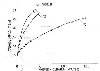
Referring now to Figures 6 and 7, these provide the variation in silicon
porosity of a particular layer with duration of quiescent immersion in
various etchants. The layer had an initial porosity of 54 * 1 % and a
thickness of 6.2 + 0.2 um and is produced by anodising p+ (0.01 to 0.04
Ohm cm) wafers in 20% ethanoic HF at 8.5 mAcm-2 for 10 minuutes. Thus
Figures 6 and 7 illustrate the variation in silicon etch rate with HF
concentration and diluent. In both figures, porosity calculated from the
results of gravimetric analysis is plotted against silicon immersion
duration for various etchant strengths. Figure 6 relates to aqueous HF
diluent and Figure 7 to ethanol HF diluent. Graphs 60, 62 and 64 in
Figure 6 show porosity/time variation for silicon in etchants consisting
of 50%, 40% and 20% aqueous HF respectively. Graphs 70, 72 and 79 in
Figure 7 show silicon porosity/time variation for respective etchants
consisting of 40% by weight aqueous HF diluted with ethanol and water to
20%, 10% and 6.7% HF. It should be noted that the abscissae of Figures 6
and 7 whilst both being immersion duration have the units of hours and
minutes respectively. Graphs 60 to 64 and 70 to 74 clearly illustrate an
increase in etch rate of HF solutions with reduction in HF content.
Comparison between graphs 60 to 64 and 70 to 74 clearly illustrates a
WO 91/0942~t~ I=~ ~~ ~' ~ 14 PCT/GB90/019 ~-
dramatic increase in etch rate when ethanol is used as diluent. The
graphs 60 to 64 and 70 to 74 therefore indicate that etch rate may be
controlled by appropriate selection of etchant concentration and diluent.
The concentration of HF in solution may be selected from a wide range eg.
6.7% to 50%.
Chemical dissolution may be achieved by immersing the wafer to be treated
in the etchant in its liquid or vapour phases. Indeed when a wafer is
immersed in liquid etchant, the liquid may not penetrate and may not wet
the pores totally or even partially. The addition of a surfactant may
therefore be necessary in order to achieve the desired etch rate. A
suitable surfactant is perfluoroalkylsulphonate which is known for use in
HF solutions in the semiconductor processing industry. It should be noted
that a surfactant, such as that indicated above, may also be added to the
electrolyte.
The foregoing description provided evidence for the creation of silicon
quantum wires based on the reproduction of properties reported for silicon
quantum dots by Furukawa et al. These properties related to pale yellow
colouration and visible red photoluminescence at photon energies well in
excess of the silicon bandgap. There is also geometrical evidence for the
production of silicon quantum wires. Porous silicon may be considered in
a simplified model as bulk silicon containing parallel cylindrical holes.
As porosity is increased by etching away cylinder walls, eventually the
wall thickness between adjacent pores becomes zero. At this point,
individual quantum wires are defined, each being the material left between
three or four neighbouring merged pores. The lowest porosity of this
idealised structure at which individual pores merge and inter-pore wall
thickness becomes zero is 78.5% irrespective of pore radius (provided
radii are equal). For four neighbouring merged pores, the wire thickness
is 2(2~-1)r. Pore radii can be less than 2 nm in p- silicon of porosity
in the region of 60% for example. It is therefore anticipated that
silicon quantum wires would be produced whenever the porosity exceeded
78.5%. In practice, because of statistical distributions of pore sizes,
'O 91 /09420 1 ~ ~ ~ ~ ~~' PCT/GB90/01901
spacings and directions, quantum wires may be expected anywhere in this
porosity region, ie near or above 78.5. It is assumed that the pores are
initially well dispersed throughout the silicon material, and that
chemical dissolution does not result in large voids spaced apart by bulk
silicon. However, well-dispersed small pores are a common feature of
anodised silicon, so the etching of such pores is reasonably expected to
increase their size in a controlled manner to produce pore overlap rather
than large voids. This is supported by the results of the BET gas
analysis.