Note: Descriptions are shown in the official language in which they were submitted.
2073272
SPECIFICATION
Title of the Invention
MICROWAVE RESONATOR OF COMPOUND OXIDE
SUPERCONDUCTOR MATERIAL
Background of the Invention
Field of the invel]tion
The present invelltioll relates to microwave resonators, and
particularly to a novel ~tructure of microwave resonators which have a
signal conductor forlne(l of a compound oxide supercoIlducting thin film.
Description of related art
Electromagnetic waves called "microwaves" or"millimetric waves"
having a wavelength ill a range of a few tens centimeters to a t`ew
millimeters can be theoretically said to be merely a part of an
electromagnetic wave spectrum, but in many cases, have been considered
from a viewpoint of an electric engineering as being a special independent
field of the e~ectromagnetic wave, since special al1d unique methods and
devices have been developed for handlillg these electromagnetic waves.
In 19~6, Bednnrz and MLiller reported (La, Ba)2CuO4 showing a
superconduction state at a temperatule of 30 K. In 1987, Chu reported
~Ba2Cu30y having a superconductinn critical temperature on the order
of 90 K, and in 198~ Maeda reported a ~o-call bismuth (Bi) type
&ompound oxide ~uperconductor material havin~ a ~uperconduction
critical temperatule exceeding l00 K. These compound oxide
superconductor matelials can obtain à superconduction condition with
2073~2
cooling using an inexpensive liquid nitlo~en. As a result, possibility Or
actual application of the superconduction technology has become discussed
and studied.
Phenomenon inherent to the superconduction can be advantageously
utilized in various applications, and the microwave component is no
exceptions. In general, the microstrip line has an attenuation coefficient
that is attributable to a resistallce component of the conductor. This
attenuation coefficient attriblJtable to the resistance component increases
in proportion to a root of a fre~uenc~,. On the other hand, the dielectric
loss increases in proportion to incleclse of the frequency. However, the
loss in a recent microstrip line is alnlost attributable to the resistance of
the conductor in a frequency region not greater than 10GHz, since the
dielectric materials have been improved. Thelefole, if the resistance of
the conductor in the strip line call be reduced, it is possible to greatly
elevate the performance of the microstrip line.
As well known, tlle microstrip line can be used as a simple signal
transmission line. In addition, if a suitable patterning is applied, the
m~crostrip line can be used as miclow~ve components inc~uding an
inductor, a filter, a resollcltol, a delay line, etc. Accordingly,
improvement of the microstl ip line ~ill lead to improvement of
characteristics of the microwave componellt. Therefore, various
microwave components havillg ~ si~nal conductor formed of an oxide
superconductor have been proposed.
A typical conventional microwave resonator using the oxide
superconducfor as mentioned above includes a first substrate provided
with a superconductillg sigllal conductor formed of ~n oxide
superconducting thin film patterned in a predetermined shape, and a
207~27~
second substrate having a whole sllrface provided with a superconducting
ground conductor also formed of an oxide superconducting thin film.
The first and second substrates are stacked on each other within a metal
package, which is encapsulated and sealed with a metal cover
The superconducting signal conductor is composed of a resonating
superconducting signal conductor, and a pair of superconducting signal
launching conductors located at opposite sides of the resonating
superconducting .signal collductor, separated from the resonatin~
superconducting signal conductor. These superconducting signal
conductor and the superconductillg ground conductol can be formed of an
superGonducting thin film of l~or example an Y-Ba-Cu-O type compound
oxide.
The microwave re~onator havin~ tlle above mentiolled construction
has a specific r esonating frequency fO in accordance with the
characteristics of the ~uperconductitlg signal conductol, and can be used
for frequency control in a loccll oscillator used in microwave
communication instrumellts, and for other pulposes.
However, one problem has been encountered in which the
resonating frequency f O of the microwave r esonator actually
manufactured by USillg the oxide superconductor is not necessarily in
consistency with a designed value. Namely, in this type microwave
resonator, a slight variation ill chal acteristics of the oxide
superconducting thin fihll and a slight error in assembling influence
mutual]y so as to cause an inevitab]e dispersion in the characteristics of
the microwave resonatol.
2 0 ~
Summary of the Invention
Accordingly, it is an object of the present invention to provide a
microwave resonator which addresses the above mentioned defect of the
prior art.
Another object of the present invention is to provide a novel
microwave resonator in which the resonating frequency of the microwave
resonator can be adjusted in order to compensate for dispersion in the
characteristics of the microwave resonator.
According to the present invention there is provided a microwave
resonator including a dielectric substrate formed of a material selected from
the group consisting of MgO, SrTiO3, NdGaO3, Y203, LaAl03, LaGaO3, Al203
and ZrO2, a patterned superconducting signal conductor provided at one
surface of said dielectric substrate and a superconducting ground conductor
provided at the other surface of said dielectric substrate, said
superconducting signal conductor and said superconducting ground
conductor each being formed of a thin film of a high critical temperature
copper-oxide type oxide superconductor material, the resonator further
including a rod adjustably positioned to be able to penetrate an
electromagnetic field created by a microwave propagation through said
superconducting signal conductor, so that the resonating frequency fo f the
microwave resonator can be adjusted by controlling the position of a tip end
of said rod.
Preferably, the rod is formed of a material selected from the group
consisting of an electric conductor such a metal, a dielectric material and
a magnetic material.
As seen from the above, the microwave resonator in accordance
with the present invention is characterized in that it has the means for
adjusting its resonating frequency fO.
- 4 -
2Q7~
When a microwave propagates through the microstrip line, an
electric field is created between the ground conductor and the signal
conductor, and at the same time, a magnetic field is created around the
signal conductor. If a conductor piece, a dielectric piece or a magnetic
piece is inserted into the electromagnetic field thus created, an
electromagnetic characteristics of the resonator, in particular, the
resonating frequency of the resonator is caused to be changed. Therefore,
the resonating frequency fO of the microwave resonator can be easily
adjusted by controlling the amount of penetration of the rod (forrned of a
conductor, a dielectric material or a magnetic material) into the
electromagnetic field.
As mentioned above, the rod for adjusting the resonating frequency
fO of the microwave resonator can be forrned of a conductor, a dielectric
material or a magnetic material, but is not limited in shape and in
composition of the material. Therefore, the rod can be easily mounted on
the microwave resonator by utilizing a package or a cover of the
microwave resonator. In this connection, the conductor piece formed of a
superconductor material can be advantageously used in order to prevent
decrease of the Q factor of the resonator.
The superconducting signal conductor layer and the
superconducting ground conductor layer of the microwave resonator in
accordance with the present invention can be formed of thin films of
a Y-Ba~u-O type compound oxide superconductor material, a
Bi-Sr-Ca-Cu-O type compound oxide superconductor material, or a
Tl-Ba-Ca-Cu-O type compound oxide superconductor material. In
addition, deposition of the oxide superconducting thin film can be
exemplified by a sputtering, a laser evaporation, etc.
r~ s
2~732~2
addition, deposition of the oxide superconducting thin film can be
exempli~led by a sputtering, a laser evapo~a~ion, etc.
The substrate is formed of a material selected from the group
consisting of MgO, SrTiO3, NdGaO3, Y203, LaAl03, LaGaO3, A1203 and Zr2-
The oxide material of the substrate should not diffuse into the high-Tc
copper-oxide type oxide superconductor material used, and should
substantially match in crystal lattice of ~e high-Tc copper-oxide type oxide
superconductor material used, so that a clear boundary is formed between
the oxide insulator thin film and the superconducting layer of the high-Tc
copper~xide type oxide superconductor material.
A preferred substrate material includes a MgO single crystal, a
SrTiO3 single crystal, a NdGaO3 single crystal substrate, a Y203, single
crystal substrate, a LaA103 single crystal, a LaGaO3 single crystal, a
A1203 single crystal, and a ZrO2 single crystal.
For example, the oxide superconductor thin filrn can be deposited
by using, for example, a (100) surface of a MgO single crystal substrate, a
(110) surface or (100) surface of a SrTiO3 single crystal substrate and a
(001) surface of a NdGaO3 single crystal substrate, as a deposition surface
on which the oxide superconductor thin film is deposited.
The above and other objects, features and advantages of the present
invention will be apparent from the following description of preferred
embodiments of the invention with reference to the accompanying
C
2U73~72
drawings However, the examples explained hereillafter are only for
illustration of the present invention, and therefore, it should be
understood that the present invention is in no way limited to the following
examples.
Brief Description of the Drawings
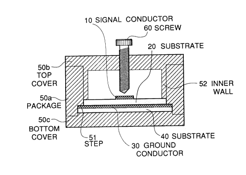
Figure 1 is a diagrammatic sectional view showing a first
embodiment of the microwave resollatol in accordance with the present
inventlon;
Figure ~ is a pattem diagram S]lOWillg the signal conductor of the
superconducting microwave resonator shown in Figure l;
Figure 3 i~ a grapll showing the characteristics of the
superconducting microwave resonator shown in Figure 1.
Figure 4 is a diagrammatic sectintlal view showing a second
embodiment of the microwave resonator in accordance with the present
invention; and
Figure 5 is an enlalged diagramlllatic sectional view of the screw
incorporated in the supercollductillg microwave resollator shown in
Figure 4.
Description of the Prefelred embodiments
Referring to Figure 1, thele is shown a diagrammatic sectional view
showing a first embodilnellt of the microwave resonator in accordance
with the present invelltioll.
The shown microwave resonator includes ~a first substrate 20
formed of a dielectric matelial and having an upper surface formed with
a superconducting si~nal conductor 10 constituted of an oxide
2073272
superconducting thin film patterned in a predetelmined shape mentioned
hereinafter, and a second substrate 40 formed of a dielectric material and
having an upper surface fully covered with a superconducting ground
conductor 30 also formed of an oxide superconducting thin film. The
first and second substrates 20 alld 40 are stacked on each other in such a
manner that an all lower surface of the first substrate 20 is in contact with
the superconducting ground conductor 30. The stacked assembly of the
first and second substrates 20 and 40 is located within a hollow package
SOa of a ~quare ~ection having upper and lower open ends. The hollow
packa~e 50a is encap~ulated and sealed at its upper and lower ends with a
top cover SOb and a bottom cover SOc, respecti~ely. The second substrate
40 lies on an upper surface of the bottom cover SOc.
Since the oxide superconductin~ thin film 10 is formed on the first
substrate 20 and the oxide superconducting thin film ~0 is formed on the
second substrate 40 independently of the first substrate 20, it is possible to
avoid deterioration of the oxide superconductillg thin films, which would
occur when a pair of oxide superconducting thin lilms are sequentially
deposited on one ~urface of a substrate and then on the other surface of
the same substrate.
As shown in Figule 1, the second substrate 40 is large in size than
the first substrate 20, and an inner surl`ace of the package SOa has a step
51 to comply with tlle differellce in size between the first substrate 20 and
the second ~ubstrate 40. Thus, the second substrate 40 is sandwiched and
fixed between the upper surface of the bottom cover 50b and the step 51
of the package SOa, in such a mannel that the superconducting ground
conductor ~0 formed on the second substrate 40 is at its periphery in
contact with the step 5~ of the package 50a.
2073~2~2
In addition, the top cover 50b has an inller wall 52 extending
downward along the inner surface of the package 50a so as to abut against
the upper surface of the first substrate 20, so that the first substrate 20 is
forcibly pushed into a clo~e contact with the the superconducting ground
conductor 30 of tl~e second substrate 40, and held between the second
substrate 40 and a lower end of the inner wall 52 of the top cover 50b.
In addition, actually, lead conductors (not shown) are provided to
penetrate throu~h the package 50a or the cover 50b in order to launch
microwave into the signal cotlductor 10.
The shown microwave resonator also includes a screw 60, which is
formed of brass and which iS screwed through the top cover 50b of the
package 50a to extend pelpendicular to the the signal conductor l0 and to
be aligned to a centel of the signal cnnductor I0. By rotating a head of
the screw 60, it is possible to cause a tip end of the screw 60 to approach
and move apart from the signal conductor l0.
Figure 2 shows a patterll of the superconducting signal conductor
10 formed on the first substrate 20 in the microw~ve resonator shown in
Figure l.
As shown in Figule 2, on the first substrate 20 there are formed a
circular superconducting ~signaJ conductol 11 to constitute a resonator,
and a pair of supercc)1lductil1~ siglla1 conductors 12 and 13 launching and
picking up the microwave to and from the superconducting signal
conductor 11. These ~uperconductillg signal conductors 11, ]2 and 13
and the superconducting grout1d coll(luctol 3~) Oll the second substrate 40
can be formed of an superconductil1g thin film of for example an
Y-Ba-Cu-O type compoulld oxide.
207327~
The microwave resollator havillg the above mentioned construction
is used by cooling the superconducting signal conductor 10 and the
superconductor ~round conductor 30 so that the conductors 10 and 30
behave as superconduc~ors. On the other hand, by handling the screw 60,
the electromagnetic characteristics of ~he resonating circuit constituted of
the superconducting signal conductor 10, the superconducting ground
conductor 30, the package 50a and the covers 50b and 50c can be
modified, and the resonatillg frequency fO of the microwave resonator
can be adjusted.
A microwave resonatol having a constructlon shown in Figure 1
was actually manufactured.
The first substrate 20 was fo~ned of a square MgO substrate having
each side of 18 mm and a thicknes~ of 1 mm. The superconducting
signal conductor ]0 was formed of a Y-Ba-Cu-O compound oxide thin
film having a thickness of 5000 A. This Y-Ba-Cu-O type compound
oxide superconductill~ thin film was deposited by a sputtering. The
deposition condition was as follows:
Target: YlBa~Cu3O7-x
Sputtering gas : Ar containing 20 mol % of 2
Ga~ pressure : 0.5 Torr
Substrate Temperature : 620C
Film thickness : 5000 ~
The ~upercondLIcting signal conductor 10 thus formed was patterned
as follows so as to constitllte tl-e resonatol: The supercollducting signal
conductor 11 is in the form of a circle having a diameter of 12 mm, and
the pair of supercolld-lctillg signal kluncl~ g conductor~ 12 and 13 have a
width of 1.0 mm and a lengtll of 1.5 mm. A distance or gap between
1 ()
î0732~2
the superconducting signcll conductor ] I and each of the superconducting
signal launching conductors ~2 and 13 is 1.5 mm at a the shortest
portion.
On the other hand, the second substrate 40 was fo~ned of square
MgO substrates having a thickness of 1 mm and each side of 20 mm.
The superconducting ground conductor 30 was formed of a Y-Ba-Cu-O
compound oxide thin film having a thickness of 5000 A, in a sputtering
similar to that for depo~ition of supercollduct;ng signal conductor 10.
The above mentioned three substrates 20 and 40 were located within
the square-sectioll hollow package 50a formed of brass, and opposite
openings of the package 50a were encapsu~ated and sealed with the covers
50b and 50c also formed of brass.
In addition, a thre~lded hole for receiving the screw 60 is formed at
a center of the upper cover 50b, and the screw 60 formed of M4(ISO)
brass is screwed into the threaded hole.
For the superconducting microwave resonator thus formed, a
frequency characteristics of the transmission power was measured by use
of a network analyzer. The resonatillg frequency at 77 K is as shown in
Figure 3.
Referring to ~igl~re 4, there is showtl a diagramrmatic sectional view
showing a second embodiment of the microwave resonator in accordatlce
with the present invelltioll. Tn Figure 4, elements similar to those shown
in Figure 1 are given the same Reference Numerals, and therefore,
explanation thereof will be omitted.
As seen from comparison between Figures l and 4, the second
embodiment has basically the same construction as that of the first
embodiment, except tllat the tip end of the screw 60 is provided with a
2~73~72
superconductol piece 61 (not showll in Figure 4) and a sleeve 62 for
holding and covering the superconductor piece 61 on the tip end of the
screw 60.
Figure S is an enlarged diagrammatic sectional view of the screw 60
incorporated in the superconducting microwave resonator shown in
Figure 4.
As shown in Pigure ~, the superconductor piece 61 has a substrate
61b in the form of a circular disc having one surface coated with an oxide
superconducting thin film 61a, wlliC]l iS formed of the same material as
those of the supercor~ducting conductor 10 or 30. The sleeve 62 is
formed of brass, which is the same material as that of the screw 60. An
upper portion of the sleeve 62 has a fema}e-threaded inner surface for
mating with the ~ower end of the screw 60, as shown in Figure 5. A
lower end of the sleeve 62 has an inner flange 62a defining an opening
havin~ an inner diameter slightly smaller than an outer diameter of the
superconductor piece 61. Thelefole, the superconductor piece 61 is
located on the tip end of tlle screw 60 in such a manner that the oxide
superconducting thin film 61a is directed toward the outside, and then, the
sleeve 62 is screwed over the tip end of the screw 60 in SUC]l a manner
that the superconductor piece 6:1 is fixed to the tip end of the screw 60
and the ilmer flange 62a of the sleeve 62 is brought into contact with the
oxide superconducting tllin film 61~. Thus, the oxide superconductin~
thin film 61a is electrically connected to the ground conductor 30 through
the sleeve 62, the screw 60, the top cover 50b, and the package 50a, all of
which are formed of brass.
With the above mentiolled arrangement, by halldling the screw 60
externally of fhe microwave resonator so as to change the amount of
~2~073272
penetration of the ~uperconductor piece 61, the electromagnetic
characteristics of the resonating circuit constituted of the superconducting
signal conductor 10, the superconducting ground conductor 30, the
package 50a and the covers 50b and 50c can be modified, and the
resonating ~requency fO of the microwave resonator can be adjusted.
A microwave re~onator havin~ a construction shown in Figures 4
and 5 was actua:~ly manufactured, and the characteristics was also
measured.
The portions of the second embodiment other than the
superconductor piece 61 and the sleeve 62 was formed in the same
manner as that for manufacturing the first embodiment.
The superconductor piece 6~ wa~ formed by CUttillg out a circular
disc having a diameter of 8 mm, from a MgO substlate 61b having a
thickness of ~ mm and deposited with a Y-Ba-Cu-O compound oxide thin
film 61 a. The deposition method and conditions for forming the
Y-Ba-Cu-O compound oxide thin film 61a and the thickness of the
Y-Ba-Cu-O compound oxide thin film 61a are the same as those for
fo~nin~ the signal conductor 10.
The sleeve 62 was manufactured by machinillg a circular brass rod
into a tubular membel havillg such a ~ize that the female-threaded portion
has an inner diameter of l0 mm, a ~ip end portion for receiving the MgO
substrate 61b has an inner diameter of 8 mm, and the inner flange 62a of
the tip end for holding the MgO substrate 61b has an inner diameter of
7.5 mm.
In order to evaluate the perfornlance of the microwave resonator of
the second embodiment, another microwave resonator using an Au thin
film in place of the Y-Ba-Cu-O compound oxide thin film 61a was
2073~7~
manufactured as a coIllparcltive sample undeI the ~ame manufacturing
conditions as those for manufacturing the microwave resonator of the
second embodiment. The Au thin film formed on the substrate 61b has a
thickness of 10 ,um.
The following shows the Q factor and the resonating frequency o
the two microwave resonators when the distance between the tip end of
the sleeve 62 and the si~nal conductor lO is adjusted at 8 mm and 2 mm,
respectively.
Distance between the screw
and the signal conductol 8 mm 2 mm
resonatillg Q resonating Q
frequency factor frequency factor
Y-Ba-Cu-O thin film 4.165GHz ]3500 4.732GHz 13800
Au thin film 4.166GHz 12800 4.735GHz 6100
As seen from the above, if the conductor piece penetrating into the
inside of the microwave resollator is formed of the superconductor, the Q
factor is stable regardless of change of the resonating frequency.
As mentioned above, the microwave resonator in accordance with
the present invention is sn con~structed as to be able to easily adjust the
resonating frequency fO. In addition~ if an appropriate conductor piece is
used, the resonating frequency can be adjusted while maintaining the Q
factor at a stable value.
Accordingly, the miclowave resonator in accordance with the
present invention can be effectively used in a local oscillator of
microwave communication instruments, and the like.
- 14 -
2073272
The invention has thus been shown and described with reference to
the specific embodiments. E~owever, it should be noted that the present
invention is in no way ]imited to the details o~ the illustrated structures
bwt changes and modifications may be made within the scope of the
appended claims.