Note: Descriptions are shown in the official language in which they were submitted.
~?~
3-199922
SUPERCONDUCTIVE CONJUGATE PHOTOCONDUCTIVE SUBSTANCES
OF THE Bi-SrCa(LaY)-Cu-O SYSTEM, A METHOD FOR
PRODUCING THE SAME AND A SUPERCONDUCTIVE
OPTOELECTRONIC DEVICES BY USING THE SAME
The present invention relates to a substance of
superconductive conjugate photoconductivity in parallel
to superconductivity in a composition range outside the
superconductive composition region within the
05 Bi-SrCa(LaY)-Cu-O oxide system and a method for
producing the same and a superconductive optoelectronic
device with the same.,
Here, I define "Superconductive-Conjugate
Photoconductivity" to be a substantially new type of
10 large photoconductivity in basic substances or host
insulators which emerges in several steps with
decreasing temperature in accordance or correspondences
with the critical temperatures of superconductivity in
relevant conductive substances, all based on the
15 discoveries and inventions disclosed by the present
inventor in that "Photoconductivity" and
"Superconductivity" are conjugate with each other in a
certain group of oxide superconductors.
The present inventor has presented series of
20 substances having photoconductivity as the substances
close to but outside of superconductive region in the
prior art, and has already filed patent applications
~ 4~5
related to substances in the Y3_xBax-Cuy-oz oxide system
of superconductive photoconductivity (Japanese Patent
Application Laid-open No. Heil(1989)-197175), to
substance in the La2-Cul-Oz system of superconductive
photoconductivity (Japanese Patent Application Laid-open
No. Heil(1989)-201059), to substance in the
Bal-Pbl_x-Bix-Oz oxide system of superconductive
photoconductivity and a method for producing the same
(Japanese Patent Application Laid-open
No. Hei2(1990)-51423) and to substance in the
Ca(x-x)-srx-Bi(y-y)-cuy-oz oxide system of superconductive
photoconductivity and a method for producing the same
(Japanese Patent Application Laid-open
No. Hei2(1990)-51424).
1~ Before 1986, superconductive materials have
signified essentially metals and alloys thereof.
However, recent oxide high temperature superconductors
(such as the Y-Ba-Cu-O oxide superconductor) are
originally insulators or semiconductor and have been
doped by using a large amount of additional elements
(such as Ba, Sr) for the purpose of increasing hole
density and improving the critical temperature.
Therefore, experiments of optical properties in the
vicinity of their optically visible range were mainly
limited to measurements of optical reflection or
scattering by reflecting metallic properties thereof.
An incident light reflects or scatters on the
surface of superconductor, but never enters into
a superconductor, so that superconductivity and optical
properties such as absorption have been usually
considered to be irrelevant, except reflection and
scattering of light, in domestic scientific societies
and international conference abroad.
The reason thereof is because superconductivity
are considered to be incompatible physical properties
with absorption and photoconductivity and the stability
of a superconductor is broken by irradiating light in
the wavelength range of shorter than those relevant to
the gap energy of the BCS theory. However, there exist
reasonably clear correlations between photoconductivity
in insulator and superconductivity in the oxide
1~ materials such as the Y-Ba-Cu-O, La-Cu-O, Ba-Pb-Bi-O
systems of oxide material and the like. Therefore, if
a substance having either one or both of deeply
correlated superconductivity and photoconductivity is
obtained, it becomes possible to utilize it to compose
devices such as an optically controllable Josephson
element or a superconductive phototransistor and the
like and eventually to manufacture apparatus such as
"superconductive optical computer" and the like having
both properties of machinery and tools of "superconduc-
tor computer" based on the presently pursued Josephson
element and of "optical computer" proposed by
optoelectronics, that is, "superconductive optical
2Q~5~
computer" and the like.
The present invention is based on the
discovery of photoconductive substances exhibiting a
normally unforeseeable photoconductive phenomenon
conjugate with superconductivity by performing an
experiment of optical properties, particularly high
speed pulse photoconductivity, of substance close to
but outside the critical composition region of
superconductive substance.
In a method for producing the
photoconductive material according to the present
invention, photoconductive substance of the
Bi2-(sr2cal)l-x(La2yl)x-cuy-oz oxide system having
photoconductivity conjugate with superconductivity of
the Bi-SrCa(LaY)-Cu-O system (x=0) superconductor can
be obtained by controlling a composition ratio x, y
and z, thereafter heat treating to select a
composition range to be y=2, and approximating to x=l
in 0.4<x<1 (preferably 0.5~x<1) or by cooling extremely
quickly.
It is an object of the present invention to
provide a superconductive conjugate photoconductive
substance having a photoconductivity Q(~,T) at a
temperature less than 105-115 K and less than 65-85 K,
upon photoexcitation in an optical wavelength (~)
range of 420-670 nm.
According to one aspect of the invention,
there is provided a superconductive-conjugate
-- 4
~3
.
~ ~ 7 3 ~ 5 5
photoconductive substance of a Bi-SrCa(LaY)-Cu-O oxide
with a composition having the general formula:
Biz-(Sr2Cal)l-X(La2Yl)x~CUy ~Z~
where 0.4<x<1, y=2 and z=9-10.5, wherein said substance
is an insulator or a semiconductor when not exposed to
light, and exhibits a photoconductivity with
superconductivity at a temperature of less than
105-115 K and at a temperature less than 65-85 K, upon
photoexcitation in an optical wavelength range of
420-670 nm.
The present invention also provides, in
another aspect thereof, a method of producing a
superconductive-conjugate photoconductive substance as
defined above. The method of the invention comprises
the steps of:
a) sintering a starting material with a
composition having the general chemical formula
Bi2-(Sr2Cal)l-X(La2Yl)x~CUy ~Z~
where 0.4<x<1, y=2 and z=9-10.5, at a temperature of
800-840~C for 8-15 hours, to cause the starting
material to undergo a solid phase reaction;
b) annealing the product obtained in
step (a) for 8-15 hours;
c) sintering the annealed product obtained
in step (b) at a temperature of 900-940~C for
8-15 hours, after forming under pressure;
d) cooling the sintered product obtained in
step (c) for 8-15 hours; and
- 4a -
~ f
~ ~3~
e) annealing the cooled product obtained in
step (d) at a cooling rate of 100-150~C/hour, to obtain
the desired superconductive-conjugate photoconductive
substance.
According to a further aspect of the
invention, there is provided a superconductive
optoelectronic device comprising:
- an insulating substrate;
- source and drain electrode regions formed
on the substrate, wherein the source and drain
electrode regions are each made of a superconductor
material which becomes superconductive below a
critical temperature thereof;
- a photoconductive gate region formed
between the source and drain electrode regions, which
is an insulator or a semiconductor when not exposed to
light, but which exhibits a photoconductivity upon
photoexcitation in an optical wavelength range of
420-670 nm, when at a temperature below the critical
temperature of said superconductor material; and
- a bias source connected between the
source and drain electrode regions;
wherein the source and drain electrode regions
comprise a superconductive material having the general
formula:
Bi2- ( Sr2Cal ) l-X ( La2Yl ) x-Cu2-0z
~ ~ ~ 3 ~ ~ ~
wherein 0<x<0.3, y=2 and z=9-10, and the
photoconductive gate region comprises a
photoconductive material having the general formula:
Bi2- ( Sr2Ca~ X ( La2Yl ) x-Cu2-0z,
wherein 0.4<x<1, y=2 and z=9-10.5, which is an
insulator or a semiconductor when not exposed to
lighti
whereby a current between the source and
drain electrodes can be controlled in correspondence
with the intensity of light incident to the
photoconductive gate region.
Once such a type of superconductive
optoelectronic device is formed with the
- 5a -
2~,'f~55
Bi2-(sr2ca~ x(La2yl)x-cuy-oz~ it must be naturally
straight forward to further develop the new field from
such a device to other devices; and eventually to
superconductive optoelectronic apparatus with the
2-(sr2cal)l-x(La2yl)x-cuy-oz system, for instance a
switching device with no power loss, an optically
operating device with no power loss, an optically
operating logical device, a space parallel type
optically operating device, a camera or an image forming
device possibly with superconducting wiring, a high-
speed optically operating apparatus to be driven at an
extremely low power with higher optical efficiency, and
the like.
The reason why the substance of the present
lb invention is limited to the composition having the
general chemical formula is because superconductive
conjugate photoconductive substance having the
superconductive conjugate temperature dependences and
the specified dependences at photoexcitation wavelength
even within an insulative composition range can be
obtained as substantially shown in embodiment only when
the substance within this composition range is heated at
a temperature of about 800-840~C for producing a solid
phase reaction for 8-15 hours, annealed for 8-15 hours,
formed with pressure, thereafter secondarily sintered at
900-940~C for 8-15 hours, and annealed at a cooling rate
of 100-150~C/H.
~5
The reason of limiting each condition of the
method for producing photoconductive substance according
to the present invention is explained. A primary
sintering step for heating at a temperature of 800-840~C
for producing a solid phase reaction of starting
material compound as described in the general chemical
formula Bi2-(Sr2Cal)l x(La2Yl)x-Cuy-Oz where 0.4_x_1,
y=2 and z=9-10.5, for 8-15 hours and annealing for
8-15 hours and a secondary sintering step after forming
under pressure, heating at 900-940~C for 8-15 hours and
annealing at 100-150~C/H are necessary steps for
completing the solid phase reaction and obtaining
a uniform solid phase. Heating at a temperature higher
than 1000~C is not preferable because it is melting.
1~ Moreover, heating at less than 900~C cannot attain
an object of completing the solid phase reaction and it
is not preferable.
For a better understanding of the invention,
reference is made to the accompanying drawings, in
which:
Fig. 1 enumerates experimental results on the
variation of powder X-ray diffraction pattern over x to
clarify crystalline structure of superconductive
conjugate photoconductive substance in the
(sr2cal)l-x(La2yl)x-cu2-oz system;
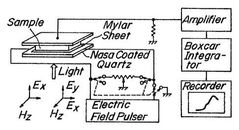
Figs. 2A, 2B and 2C are the schematic diagrams
of circuit and time sequence for the repetitive
measurement of pulse photoconductivit~-b~ blocking
electrodes;
Figs. 3A, 3B and 3C are the sectional view of
a microwave SQUID and the blocking diagrams for the
measurement of static magnetization;
Fig. 4A indicates characteristic data of
wavelength dependence of photoconductive response Q(A,T)
of the basic substance Bi2O3, and Fig. 4B indicates
characteristic data of a wavelength dependence of
photoconductive response Q(A,T) of a specimen of
Bi 2La2ycu2oz;
Fig. 5A is a characteristic plotting to
exemplify the relation between temperature and
photoconductive response Q(A,T) of the basic substance
1~ Bi203(#BO3). Fig. 5B is a characteristic graph showing
the relation between temperature and photoconductive
response Q(A,T) of the basic substance Bi203:M2+(#S213).
Fig. SC is a characteristic graph showing the relation
between temperature and photoconductive response of
2(sr2ca~ x(La2yl)xcu2oz for x=l as photoconductive
substance, and Fig. 5D iS a graph showing the relation
between temperature and resistance in the dark of the
Bi2(sr2cal)l-x(La2yl)xcu2oz for x=O as a superconductive
substance;
Fig. 6 displays characteristic plottings to
indicate the temperature dependence of dark
resistivity p(T) (mQ-cm) in the region of x=0-0.4 of
~55
the Bi2(Sr2Ca~ x(La2Yl)xCu20z system;
Fig. 7 displays characteristic plottings to
indicate the temperature dependence of photoconductive
response Q(T,A) in the region of x=O.9-1.0 of the
0~ Bi2(Sr2Cal)l x(La2Yl)xCu2oz system;
Fig. 8 is a quasi-phase diagram to exhibit the
emergence or step temperature Tps of photoconductivity
and superconductive transition temperature Tsc of the
Bi2(sr2cal)l-x(La2yl)xcu2oz system as a function of x;
Fig. 9 is a similar quasi-phase diagram to
exhibit the superconductive transition temperature Tsc
and the emergence or step temperature Tps of photo-
conductivity of the Bi2-Sr2-Cal_xYx-Cu2-oz system as
a function of x;
16 Fig. lOA is a schematic diagram of the state
density N(E) as a function of energy E of the
Bi2(sr2cal)l-x(La2yl)xcu2oz system in the case of x=l,
and Fig. lOB is a schematic diagram of the state density
N(E) as a function of energy E of the
2(sr2cal)l-x(La2yl)xcu2oz system in the case of x=O;
Fig. 11 is a schematic cross section to
exemplify an embodiment of the construction of the
superconductive optoelectronic element according to the
present invention;
Fig. 12 is a schematic diagram to display
an embodiment of the construction of the superconductive
optoelectronic device according to the present
invention; and
Figs. 13A and 13B are a schematic diagram to
illustrate the construction of the spatial parallel
operation device with the use of the superconductive
optoelectronic element alley according to the present
invention.
The greater part of hitherto known the
Ba-Pb-Bi-O, La-Cu-O, Y-Ba-Cu-O and Bi-Sr-Ca-Cu-O systems
of oxide compounds are usually insulators or semi-
conductors in the ground state, that is, in the dark(i.e. in a dark place condition), particularly with no
irradiation at low temperature. Therefore, it is
possible to create the elementary excitation by giving
a suitable energy with a suitable kinetic momentum above
1~ the ground state of these substances. It has been
presumed that an elementary excitation exceeding
an energy gap merely breaks the ground state of
a superconductor in the BCS theory. However,
an insulative semiconductor has a possibility of
creating an elementary excitation in coherent state in
the conduction and/or valence bands such as a bipolaron
and an exciton above the ground state even in
a thermally non-equilibrium state. These study has been
made in parallel with a study of a superconductor of
a high critical temperature Tc. Apart from a trend of
the study, however, the present invention has been
completed by finding a superconductive conjugate photo-
- 10 -
t'.,J~S~
conductive substance correlative with a superconductive
substance to elicit the photoconductivity Q(A,T) at
photoexcitation of the specified range of optical
wavelength A at temperature below a critical temperature
Tsc outside of the composition of superconductors.
This is a new finding in the fields of fundamental
physics and applied physics from a novel point of view,
that is, from the viewpoint of an elementary excitation
concept.
In the present invention, the reason why the
composition of superconductive conjugate oxide
photoconductive substance is limited to the general
chemical formula
Bi2- ( Sr2Ca~ X ( La2Yl ) x~CUy~Oz
1~ where 0.4_x'1, y=2, and z=9-10.5, is because since the
composition of x=0-0.3 is the condition to be a super-
conductor, so that the composition of superconductor
range x=0-0.3 is as shown in Fig. 6 excluded.
The inventor studied and examined with the region of
substance of 0.4'x_1 having a composition close to
a superconductor and having a temperature dependence of
photoconductivity conjugate with superconductivity
within a range where the substance does not become
a superconductor. There was a discovery of a fact that
the substance of an insulator or a semiconductor for
0.4_x'1.0 in the dark reveals photoconductivity having
a temperature dependence in parallel to or conjugate
- 11 -
with superconductivity at photoexcitation in a specified
wavelength range of 420-670 nm.
The first step of study of the present inven-
tion is based on a fact that since even Bi2O3 has
photoconductivity to visible light of specified
wavelength, Bi2O3 was recognized as the basic substance.
Thus, the inventor examined whether any photoconductive
substance conjugate with superconductivity is obtained
by adding what additional element, and further examined
a system adding Ca, Sr with Cu and the like to Bi2O3.
As a result, the inventor found a system of photo-
conductive substance consisting of the composition
having the above general chemical formula which
composition is close to but outside of a superconductor
1~ and inherently an insulator or a semiconductor in the
dark and having photoconductivity Q(A,T) conjugate with
superconductivity at a temperature (T) of less than the
critical temperature of the superconductor at
photoexcitation in a specified wavelength range A.
The range of 0.4_x'-1, y=2, and z=9-10.5 in the
above general chemical formula
Bi2-(sr2ca~ x(La2yl)x-cuy-oz is a composition for
condition of photoconductive substance conjugate with
superconductivity of the present invention. Here, when
x=l, Bi2-(La2Yl)l-Cuy-Oz, and this composition is most
suitable for the condition of the present invention.
-12-
~J S
[Embodiment]
An embodiment of such photoconductive substance
is described. The present inventor has studied a series
of specimens in the Bi2(Sr2Ca~ x(La2Yl)x-Cuyoz system
where 0.4_x_1, y=2, and z=9-10.5, particularly
a variation of the step temperatures Tps in Q(T,A) and
TSC in p(T) over x, namely, an influence of the
composition of lanthanum (La) and yttrium (Y) to form
a quasi-phase diagram. Here, the present inventor
performed a systematic study not only of a super-
conductive phase but also of a semiconductor phase or
an insulator phase of the said substance. A large
number of specimens of Bi2-(Sr2Cal)l x(La2Yl)x-Cuyoz
system were prepared from the powder of CaCO3, SrCO3,
1~ Bi2~3, CuO, La2O3 and Y2O3. The compositions x and y of
the starting material were thoroughly examined, and
here, it became clear that x can be controlled
particularly at the composition of y=2. An oxygen
content z can also be controlled to some extent by
controlling a secondary sintering temperature and
a cooling rate. Specimen No. S235 (x=l) was prepared by
mixing 1.314 g of Bi2O3, 0.449 g of CuO, 0.918 g of
La2O3 and 0.318 g of Y2O3 and firing the mixture to be
the formula Bi2La2YlCu2Oz. Specimen No. S228 (x=0.1)
was prepared by mixing 1.329 g of Bi2O3, 0.758 g of
SrCO3, 0.257 g of CaCO3 and 0.453 g of CuO, 0.094 g of
La2O3 and 0.033 g of Y2O3 and firing the mixture to be
-13-
" 1~ ~ IQ~C ,~
~f ~J .
the formula Bi2(Sr2Cal)o. 9 (La2Yl)o.lCu2Oz, where z shows
an oxygen amount, and z changes to z=9-10.5 by
controlling the firing temperature and cooling rate,
thereby differing physical properties of a product
obtained.
In the present invention, raw materials were
compounded according to a compounding composition ratio,
thoroughly stirred, ground, thereafter primarily
sintered at 800-840~C, preferably 820~C for 8-15 hours
preferably over 10 hours to carry out a solid phase
reaction, annealed for 8-15 hours, and thereafter the
resulting product was used for preparing pellets by
forming under pressure. Moreover, these pellets were
secondarily sintered at 900-940~C, preferably 920~C for
16 8-lS hours, more preferably over 10 hours, and annealed
to room temperature at 100-200~C/H. In this manner, the
former (x=l) reveals a superconductive conjugate
photoconductive phase of 80 K class, while the latter
(x=0.1) reveals a superconductive phase of 80~110 K
class.
An embodiment of preparing the same specimens
with the other compositions is as shown in Table 1.
Moreover, the informations of their crystal structures
are displayed with performing several X-ray analyses in
Fig. 1.
-14-
Table 1
Bi 2 ( Sr2Ca~ X ( La2Yl ) zCU20Z
Primary sintering Secondary sintering
. temper- temper-
Spec Bi2o3(6N) SrCO3(4.5N) CaCO(3N) Cu0(3N) La2O3(4N) Y2O3(5N) tlme ature tlme ature
x men (g) (g) (g) (g) (g) (g) (hr) (~C) (hr) (~C)
(A) (B) (C) (D) (A) (B) (C) (T)
0.10 S-228 1.329 0.758 0.2570.4530.094 0.033 2, 10, 10(820) 2, 10, 8(920)
0.20 S-229 1.360 0.690 0.2340.4640.190 0.066 2, 10, 10(820) 2, 10, 8(920)
~ 0.30 S-230 1.351 0.599 0.2030.4610.283 0.098 2, 10, 10(820) 2, 10, 8(920)
cn
0.40 S-231 1.347 0.512 0.1780.4600.376 0.131 2, 10, 10(820) 2, 10, 8(920)
0.50 Y-4 1.118 0.354 0.1200.3820.391 0.135 2, 10, 10(820) 2, 10, 8(290)
0.60 S-233 1.336 0.338 0.1150.4560.561 0.195 2, 10, 10(820) 2, 10, 8(920)
0.80 S-234 1.325 0.167 0.0560.4520.741 0.256 2, 10, 10(820) 2, 10, 8(920) ~J
0.90 S-237 1.319 0.084 0.0280.4500.829 0.288 2, 10, 10(820) 2, 10, 8(920)
0.95 S-238 1.316 0.041 0.0140.4500.875 0.302 2, 10, 10(820) 2, 10, 8(920)
C
1.00 S-235 1.314 0 0 0.449 0.918 0.318 2, 10, 10(820) 2, 10, 8(920)
Note) Both primary sintering and secondary sintering were carried out in air.
Moreover, indication of A, B, C and D shows the step of heating A (hour), increasing
a temperature from room temperature to T (~C), keeping the temperature for B
(hour), and thereafter lowering the temperature to room temperature by taking C
(hour).
~a ~ ~ S
A phase diagram of the
Bi2-(sr2ca~ x(La2yl)x-cuy-oz system oxide compound is
a seven-element system, which is not yet complete at
a preliminary stage. Particularly important is control
of z for the oxygen deficiency corresponding to a set of
composition ratios of x and y. In spite of many
scientists' remarkable efforts, it will take some more
time to completes it. The inventor has been interested
in not only a superconductive phase but also a photo-
conductivity in a semiconductor phase and an insulatorphase in the dark. Many specimens of oxide compound in
the Bi-(SrCa)(LaY)-Cu-O system were prepared from powder
of Bi203, SrC03, CaC03, CuO, La203 and Y203.
The inventor has studied the composition of material,
1~ the annealing and quenching processes and the like in
detail, and can control to some extent for oxygen
deficiency.
Since specimens of oxide compound in the
Bi2-(sr2cal)l-x(La2yl)x-cuy-oz system are highly
insulative at certain values of x,y and z or
semiconductive at least at low temperature which are
correlative with or conjugate with superconductivity,
the inventor adopted two types of techniques for
resistivity and/or conductivity measurement in
experiment. First, it turned out that the fast pulse
technique (see Fig. 2A) with blocking electrodes
overcomes several difficult problems in the measurement
QSS
of an insulating specimen (p_108 Q cm), such as
Specimen No. S235 at temperatures down to 4.2 K from
300 K. Moreover, an electrode arrangement of lateral
mode was employed, if circumstances require (see
Fig. 2B). In measurement, an electric field pulse E was
sustained at a certain value up to E~5 KV/cm with
10 msec duration in a repetition rate of 13 Hz.
Photoexcitation by using a dye laser pulse of 3 nsec in
width was synchronized at a suitable time within the
time duration of applied electric field pulse (see
Fig. 2C).
Second, for a specimen having proper conduc-
tivity (p_101 Q-cm) such as Specimen No. S231, the
inventor adopted a usual four terminal method in the
1~ resistance measurement in the dark without photo-
excitation (e.g. installed at a specimen holder in
a cryostat).
Static magnetic susceptibility or magnitude of
magnetization M (T,H) can be measured at a weak field up
to H~500 Oe by using a microwave SQUID at 9 GHz band.
Characteristic features of this measurement are
separately described (see Figs. 3A, 3B and 3C).
In the case of photoconductivity measurement,
a specimen was photoexcited at a wavelength range of
A=420-470 nm with the use of a pulsed dye laser.
Spectral response was carefully examined by paying
strict attention. A number of excited photocarriers is
2~ ~5
of the order of 106~103 but the density can be 10l2 Q/cm3
within a thin layer of 10-3-10-4 cm in the vicinity of
a surface when an absorption coefficient is larger.
Photoconductivity signals were detected by
0~ a synchronized mode with the use of a Boxcar integrator.
A specimen of Bi2(Sr2Cal)lCu2Oz (x=0) such as
Specimen No. S182 looks black, and resistance at room
temperature is usually of the order of p<l0-1 Q cm.
According to the inventor's observation, when repetitive
pulse technique is applied to Specimen No. S235 (x=l,
insulator), a signal of photoconductivity emerges at and
grows below 80-110 K or 40-60 K. Origins of these
emergences are probably different each other.
Fist, the dependence of photoconductivity
1~ Q(A,T,E) on the applied electric field E is almost
linear up to E~4 kV/cm at T=4.2 K. Fig. 4A is the
typical spectra response of pulse photoconductivity
Q(A,T) of Specimen No. BO3 of Bi2O3, and Fig. 4B is the
typical spectra response of pulse photoconductivity
Q(A,T) of Specimen No. S235 (x=l) of Bi2-La2yl-cu2-oz
over a wavelength region of A~420-670 nm. In this
connection, Fig. 4A is new datum of photoconductivity
spectra corresponding to light absorption of Bi2O3 first
observed by the inventor throughout the world and should
be used as a standard.
Secondly, the temperature dependences of
photoconductivity Q(A,T) at the wavelength range
-18-
z'~ s
A=420-680 nm were examined for Specimen No. B03 of Bi2O3
as shown in Fig. 5A, for Specimen No. S213 of Bi2O3:M2+,
as shown in Fig. 5B and for Specimen No. S195 of
an insulator Bi2(La2Yl)Cu2Oz as displayed in Fig. 5C.
It is surprising to recognize that conspicuous
similarities definitely exist among general charac-
teristics of mutually interrelated photoconductivities
Q(A,T) of Specimen Nos. B03, S213 and Specimen
Nos. S195, S235 (x=l in Fig. 7). No one can fail to
recognize that "photoconductive response Q(A,T)" in
specimens of an insulator or a semiconductor emerges at
an absolute temperature below 80-110 K and less than
40-60 K together with the lowering of a temperature
monotonously increases and thereafter further increases
1~ at a temperature of less than 10 K, as if super-
conductivity latently underlies.
Actually, Fig. 5D exemplified the dark
resistivity p(T) of Specimen No. S182 of superconductor
Bi2(Sr2Cal)lCu2-Oz as a function of temperature.
One can immediately note that Specimen No. S182 becomes
superconductor at and below T=80-110 K and T=65-85 K.
With a slight shift in T, the photoconductive response
Q(A,T) displayed in Fig. 5C has a surprisingly well one
to one correspondence thereto.
Figs. 4 and 5 only illustrate the cases for x=0
and x=l as the both ends of the
si2-(sr2ca~ x(La2yl)x-cu2-oz system for the sake of
-19-
~_, I .~J~J~
definiteness. In general, the condition is rather
complicated in 0<x<1.
Specimen No. S182 (x=0) of Bi2Sr2CaCu2O2 is
a known superconductor. When the composition is changed
0~ from x=0 to x=l in the order shown in Table 1, the
crystalline structure varies as shown in Fig. 1, but it
becomes rather simpler in S235 (x=l).
On the other hand, the temperature dependence
of resistance p(T) of these series in the dark
drastically varies as shown in Fig. 6. As the
composition x increases from x=0 to x=0.3, the absolute
value of p(T) becomes large and the superconductive
critical temperature Tsc simultaneously becomes lower.
Further increase of x in the composition does convert
16 the specimen into a semiconductive phase at 0.3<x<0.4.
When x is even further increased, the value of p becomes
larger, the materials in that composition become
insulators. Eventually, it becomes extremely difficult
to measure resistance in the dark by a usual four-probes
method. This difficulty in the measurement results from
conditions peculiar to high resistance substance, such
as non-ohmic properties of contact electrode, formation
of space charge and tiny signal to noise (S/N) ratio due
to a low concentration of carriers.
Therefore, for a conductivity measurement of
specimens in these regions, one has to adopt the
transient technique of pulsed photoconductivity
-20-
~Y~ ~ . .~ 5
measurement with blocking electrodes, the principle of
which is explained in Figs. 2A and 2B. This method is
effective to a measurement of rather high impedance
materials. Actually, as shown in Fig. 7 in case of the
specimens for O.9_x_1, the photoconductivity signal
Q(T,A) at photoexcitation with wavelength A=476~500 nm
becomes observable at and below a certain temperature
Tpc.
It should be noted here that the value of Tsc
once decreases as x increases from x=0 to x=0.3 in the
superconductive region, and revealing photoconductivity
after superconductor insulator transition, the value of
Tpc increases again in the region from x=0.9 to x=lØ
These situations are illustrated in Fig. 8 in a form of
1~ a phase diagram like scheme for the
Bi2-(sr2ca~ x(La2yl)x-cu2oz system.
Fig. 9 displays a similar diagram for the
Bi2-sr2(cal)l-xyx-cu2-oz system in the same manner as in
Fig. 8. In this case, it is known that the lattice
spacing continuously varies by x, but the crystalline
structure never changes. Photoconductivity emerges only
in the vicinity of x=0.
In any case, both superconductive and
photoconductive regions have several values of the
critical temperatures Tsc and the emergence or step
temperatures Tps, respectively. The values of Tsc and
Tps, vary with x. They slightly shift but correspond to
each other across their transition regions.
It is not easy to simply understand these
experimental facts. It must turn out that a heating
effect of the specimen by photoexcitation is
sufficiently small when if we carefully examine and
estimate the effect. Specimen Nos. S195 and 235 of
Bi2-La2Yl-Cu2-Oz (x=l) are a semiconductor or rather
an insulator even at T=300 K. However, one can mainly
conceive that "photoconductivity" observed by using the
transient technique with the arrangement of blocking
electrodes and "superconductivity" in Specimen No. S182
of a superconductor are profoundly correlated.
As illustrated in Figs. 4A, 4B and Figs. 5A, 5B, 5C and
5D, this is probably, due to a potentiality of the
1~ insulator portions within the specimen to be convertible
to superconductor by doping. However, surprising is
an existence of such fact that even in an insulator
Specimen No. S195, there is an "emergence of
superconductive conjugate photoconductive phenomenon" to
reveal an implicit correlation as if superconductivity
latently underlies.
A specimen of the Bi2-(Sr2Ca3)l x~La2Yl)x-Cuy-oz
system in the semiconductor or insulator region is
usually gray in color. A photoconductive spectral
response Q(A,T) shown in Figs. 4A and 4B suggests that
there exists a region similar to Bi203 even not
necessarily in atomic layers but to some extent within
-22-
?~S
the inside of the specimens of the
Bi2-(Sr2Ca~ x(La2Y1)x-Oz system.
Optical absorption and photoconductivity of
Bi2O3 itself have not been sufficiently clarified yet
06 even by an experiment or an exciton theory. However,
an exciton here is considered to be a typical example of
Frenkel exciton due to charge transfer within a cation
shell and neighboring cation cells. The position of
fine structure in photoconductivity Q(A,T) of the above-
mentioned Bi-(SrCa)(LaY)-Cu-O system reasonably
coincides with the fundamental absorption edge
structures of the basic substance Bi2O3. One recognizes
several conspicuous fine structures to be considered due
to excitons. For instance, the spectra of photoconduc-
16 tive response of Bi2-La2yl-cu2-oz are similar to that of
the reference substance Bi2O3. In the vicinity of
A=568-580 nm in this spectra, we recognize a structure
which is considered to correspond to the n=2 state in
an exciton series of Bi2O3. Namely, there exists
a phase similar to Bi2O3 at least in a finite proportion
in the substance of the Bi-(SrCa)(LaY)-Cu-O system,
which no one can ignore. Crystalline structures are
slightly different from each other, but photoexcited
conduction electrons and the holes are dissociated and
26 definitely mobile (see Fig. 10A).
A conduction electron and a hole in the
standard type Bi2O3 crystal are considered to form
-23-
v~5
a rather "small polaron" in terms of the coupling
constant ~. In any case, "an emergence of
photoconductivity Q(A,T)" in insulating specimen clearly
relates to "an emergence of superconductivity", and as
if superconductivity is latently conjugate with
a photoconductive phenomenon. Therefore, the polaron
effect is at least potentially of remarkably importance
as shown in Figs. 4A, 4B and Figs. 5A-D, whether it is
a "large polaron" based on the interaction with LO
(longitudinal optical type) phonon or a "small polaron"
due to the Jahn-Teller effect or an intermediate
coupling region based on both effects as well as the
"polaron effect due to electronic polarization".
Dynamical polaron effects are considered to be effective
1~ in a coherently hybridized form of elementary
excitations. It is necessary to pay special attention
to polarons due to electronic polarization, which are
also referred to as "excitonic polarons". By examining
these experimental results, we recognize a close
relation between polarons and excitons.
As shown in Fig. lOA, these polarons and
excitons had yielded out of the optical interband
transition from the hybridized valence band state of O
(2p) and Bi(6s) or Bi(6p) conduction band (possibly
mixed with the Cu(4s,3d) (not shown) depending on case)
leaving a hole (white circle) in the 0(2p)6Bi(6s)l state
with LO phonon interaction. However, as shown in
-24-
~ 5S
Fig. lOB (x=O), a polaron in the Bi-(SrCa)(LaY)-Cu-O can
be created not by optical excitation but by substitution
of (La2Yl) by Sr2Cal. Here, Fig. lOB shows the case of
a superconductor with x=O, which already has been known.
There has recently been proposed that the hybridized
valence electron state is caused by 0(2p)Bi(6p), and the
conduction band is caused by Bi(6d). Situation here,
however, remains without substantial change.
Holes in the hybridized bands of 0(2p) and
Bi(6s) in Bi2-(sr2cal)l-x(Lay)x-cuy-oz can be created
from the ground state of a many-body system either by
an interband optical transition or by doping additional
element together with interband excitation. But, here,
a correlation effect between electrons is extremely
important in any case. One must pay serious attention
not only to the dynamical valence fluctuation between
Bi3+ and Bi4+ and between CU2+ and Cu3+, but also further
to the dynamical valence fluctuation between Cul+ and
Cu2+, particularly between Bi3+ and Bi5+. Therefore, to
clarify the mechanism of high-Tc superconductivity,
there exists a sufficient reason to consider a potential
role of an ensemble of polarons, whether large or small,
particularly an ensemble of polarons closely associated
with excitons. The ensemble of the united polarons and
excitons here is considered to be a set of bipolarons
and polaronic excitons and/or excitonic polarons due to
the dynamical electron-phonon interaction and the
-25-
dynamical electron correlation, namely, "exciton-
mediated bipolaron". As shown in Fig. 4B, it was
confirmed that the photoconductive responses Q(A,T) of
the Bi-(SrCa)(LaY)-Cu-O system have wavelength
dependence in the region of 420-670 nm similar to the
photoconductive spectra of the basic substance Bi2O3
shown in Fig. 4A. Therefore, by studying the elementary
excitations, we can approach to clarify the nature of
the superconductive ground state, irrespective of
an enormous difference in the carrier densities. To our
knowledge, the present invention based on these
experimental results is the first experimental
confirmation that the Bi-(SrCa)(LaY)-Cu-O oxide system
consists of superconductive conjugate photoconductive
1~ substance with real superconductors. It was exper-
imentally and clearly confirmed that the mechanism due
to the polarons and excitons underlies inherently
commonly over the present substances and the oxide-
series high temperature superconductor.
In case of studying the physical properties of
the Bi-(SrCa)(LaY)-Cu-O superconductive photoconductive
substance according to the present invention, the
inventor has found that the critical temperatures
115 K-105 K (high Tc phase) and 85-65 K (low Tc phase)
for starting superconductivity expected in the known
superconductor well correspond to the temperature for
revealing the superconductivity and the temperature for
-26-
2~
revealing photoresponse in the superconductive conjugate
photoconductive substance according to the present
invention.
The inventor has found for the first time that
the Bi-(SrCa)(LaY)-Cu-O oxide superconductive photo-
conductive substance has profound correlation (to
"superconductivity" at x=0 and "conjugate photoconduc-
tivity" in the proximity of x=l) by the above selection
of x. Therefore, the inventor reconfirmed the existence
of the dynamical mechanism due to polaron and exciton in
high temperature superconductivity, that is, the
dynamical mechanism due to "exciton-mediated
bipolarons".
Fig. 11 is a schematic cross section to
1~ exemplify constructed form of a superconductive opto-
electronic element according to the present invention.
In the present embodiment, we can explain the case to
devise the element as a superconductive phototransistor
(VG~ O ) . On the substrate 1, e.g., made of SrTiO3, is
formed a photoconductive gate region 2. The gate region
2 comprises a superconductive-conjugate photoconductive
Bi-(SrCa)(LaY)CuO layer of 0.2 ~m-1.0 mm in width and
1-10 ~m in thickness. This Bi-(SrCa)(LaY)CuO layer
provides special photoconductivity at and below
a critical temperature of 105-115 K and 65-85 K of
a certain superconductive material consisting of
Bi-(SrCa)(LaY)CuO at photoexcitation in the wavelength
s~s
region of 420-670 nm. On both sides of the gate region
2 are formed a source region 3 and a drain region 4.
These source region 3 and drain region 4 are composed of
a Ba(SrCa)(LaY)CuO superconductive layer showing
superconductivity at and below a critical temperature of
105-115 (K) and 65-85 K. Moreover, on the gate region
2, the source region 3 and the drain region 4 is formed
an SiO2 layer 5 of 1 ~m in thickness with optically
transparent and electrically insulating properties, and
a NESA glass layer 6 with bias electrodes is formed
thereon. Between the bias electrode on the NESA glass
layer and the source region 3 is connected a bias source
VG and between the source region 3 and the drain region
4 are connected a bias source VSD and an output
16 resistance R. In addition, it is possible to construct
the regions 3, 4 of superconductive Ba(SrCa)(LaY)CuO
system from the photoconductive Ba(SrCa)(LaY)CuO region
2 by continuously varying the composition x of (LaY) in
the Ba-(SrCa)(LaY)CuO superconductive photoconductive
substance from x=l to 0.4 and to x=0.
When such a superconductive optoelectronic
element prepared via the above process of construction
is cooled down to and below the critical temperatures of
105-115 (K) of a material layer of Ba-(SrCa)(LaY)CuO and
the temperature below 65-85 K with an incident light of
an excitation wavelength range, photocarriers density in
proportion to the intensity of incident light are
-28-
~ 3;~
realized in the gate region 2. The photocarriers
accelerated by the bias VSD between the source and drain
yield a current and result in an output voltage across
the output resistance R. Moreover, the density of
photocarriers is controlled via the light intensity and
the bias source VG, SO that the bias source VG can be
set appropriately in accordance with a purpose. With
the above construction, it is possible to obtain
an output characteristics in accordance with the
incident light intensity, so as to realize a super-
conductive optical switching element. The source region
and the drain region are particularly made of super-
conductive material, so that a substantially new
superconductive optoelectronic element can be realized
lb without heat dissipation during operation.
Fig. 12 is a schematic diagram showing
an embodiment of integrating the superconductive
optoelectronic elements shown in Fig. 11 in the form of
an alley. When the superconductive optoelectronic
elements according to the present invention are
integrated at high density in the form of one
dimensional or two dimensional alley, it is possible to
materialize a device like a camera by minimizing heat
dissipation during operation with appropriate
superconductive wirings among various elements as
a background. It is also possible to materialize the
main portions for signal detection in an optical
-29-
computer for performing a spatially parallel operation.
There is also a possibility of multi-channel operation
by selecting the wavelength of an incident light source
used.
Figs. 13A and 13B schematically illustrate
an embodiment of optical operation in the projection-
correlation optical system of the spatially parallel
optical computer [see T. Yatagai: OYO BUTSURI (Applied
Physics in Japanese), 57 (1988) p. 1136] with the use of
superconductive optoelectronic elements according to the
present invention. A plurality of optical signals made
in parallel from an alley-like light source 10 are
projected onto an encoded image mask pattern 11.
The image mask pattern 11 carries encoded image
1~ information in a mask fashion. A plurality of light
beams passed through the encoded image mask pattern 11
are incident in parallel to each element corresponding
to a composite mask optical element alley 13 via
a correlation image screen 12. Since an encoded signal
modulated by the mask screen is formed in each optical
element, an operation result is obtained from
photoelectric output signal from each optical element.
If each element of the optical element alley 13 is
constructed with the superconductive optoelectronic
element according to the present invention, it is
possible to carry out a parallel optical operation under
the condition of minimizing heat dissipation during the
-30-
operation.
The embodiment described above represents the
three-terminal element as an example, but a two-terminal
element also can be realized. Thus, the photocarrier
created at VG=O may be influenced by a superconductive
proximity effect irrespective of a small coherence
length via superconductive photoconductivity, so that
the superconductive optoelectronic element can be served
as a superconductive Josephson junction element based on
light irradiation. Such a two-terminal element can hold
a position as "superconductive photoconductive or
optically controlled Josephson junction device".
In this case, it is necessary to appropriately select
gate width and incident light amount.
lG It is possible to arrive at the following
conclusion from these results. As a result of extensive
studies, by applying not only the D.C. 4-probe method
but also method of the repetitive pulse photoconduc-
tivity measurement for studying transport phenomena in
the temperature range of T=4.2 K-300 K, and by using the
microwave SQUID for static magnetization measurement,
the inventor confirmed that "photoconductivity" is
closely correlated and conjugated with "superconduc-
tivity (zero resistance and diamagnetism)" and invented
2G "the superconductive conjugate photoconductive substance
Bi2-(sr2ca~ x(La2yl)x-cuy-oz system", 0.4_x_1, y=2 and
z=9-10.5, and also invented a method for producing the
-31-
~17~55
same. Besides, the inventor invented a superconductive
optoelectronic element and device by using the same.
The present invention has been developed in parallel
with such theoretical consideration that "dynamical
mechanism due to polaron and excitons", namely, the
mechanism due to "exciton-mediated bipolarons", is
proposed for "the high temperature superconductivity",
and these new materials will develop the up-to-date
scientific technical field of "superconductive
lU optoelectronics" which directly controls
superconductivity by light.
Although the invention has been described with
a certain degree of particularity, it is understood that
the present disclosure has been made only by way of
1~ example and that numerous change in details may be
resorted to without departing from the scope of the
invention as hereinafter claimed.
ao
26
-32-