Note: Descriptions are shown in the official language in which they were submitted.
2074 1 1 5
OUTPUT LEVEL CONTROL CIRCUIT
FOR USE IN RF TRANSMITTER
BACKGROUND OF THE INVENTION
The present invention relates to an output level
control circuit for a radio-frequency transmitter, and
more particularly to an output level control circuit
for a radio-frequency transmitter which intermittently
transmits a radio-frequency signal such as a transmitter
in a digital cellular mobile telephone system or the like.
An output level control circuit which maintains
the transmit power of a radio-frequency transmitter at
a predetermined output level comprises a radio-frequency
signal detector (referred to as a signal detector herein-
after) which detects the peak level of a radio-frequency
signal outputted from a variable gain amplifier unit.
The control circuit also comprises a comparator unit which
compares the output of the signal detector and a reference
voltage corresponding to the predetermined output level,
and a control unit which controls the output level of the
variable gain amplifier unit in response to the output of
the comparator unit.
In order to maintain the amplifier's output at a
constant level over a wide range of temperature, the
signal detector is required to be able to detect with
high accuracy the radio-frequency power level over a
2074ll5
_ - 2 -
wide range of temperature. A signal detector of this
type is disclosed in United States Patent No. 4,523,155
(issued on ll June, 1985),-which detector is aimed at
satisfying the above-mentioned requirement. The disclosed
signal detector includes a detecting diode which produces
a detection output in response to the envelope of the
radio-frequency signal, and a temperature compensating
diode which has characteristics substantially the same as
those of the detecting diode and is thermally connected to
the detecting diode. In this signal detector, a forward
- bias voltage is supplied to the detecting diode via a bias
voltage setting resistor from a bias voltage supply source.
The detected a signal is obtained as the superposition
of the detected voltage and the bias voltage via a load
resistor connected to the detecting diode. The forward
bias voltage is also supplied to the temperature
compensating diode from the bias voltage supply source,
wherein the voltage of the bias voltage supply source
is changed accompanying the variations in the forward
voltage of the temperature compensating diode. Since
the bias voltage of the detecting diode is the result of
subtracting the forward voltage of the detecting diode
from the voltage of the bias voltage supply source, it
will be canceled by the temperature variations of the
forward voltage of the temperature compensating diode
even if it contains temperature variations. Accordingly,
2074 1 1 5
_ - 3 -
this signal detector is capable of producing a detected
signal which is not affected by the changes in the
temperature.
The comparator unit compares the reference voltage
that corresponds to a predetermined output level of an
intermittent transmitting signal with the voltage of the
detected signal, and the comparison output is supplied
to the control unit. The control unit controls the gain
of the variable gain amplifier unit so as to bring the
detected signal to conform with the reference voltage.
- When the reference voltage is raised or lowered, the
detected signal, which corresponds to the output level
of the transmitting signal, has to quickly follow the
raised or lowered reference voltage. For example, in
accordance with the recommended standard (EIA Interim
Standard, IS-l9-B, 3.1.3.3, January 1988, U.S.A.) for
the 800 MHz cellular subscriber units of the EIA system,
it is prescribed that the rise and the fall times of the
transmitting signal be less than 2 milliseconds.
Since, however, the above-mentioned output level
control circuit carries out the control of the output
level, at the time of the rise of the transmitting signal,
only when the reference voltage is higher than the signal
detector output, it is not possible to perform the control
of the output level until the reference voltage becomes
higher than the bias voltage of the detecting diode when
20741 1 5
_ - 4 -
a bias voltage is applied to the detecting diode for the
purpose of temperature compensation as mentioned above.
Consequently, at the time of starting transmitting radio
power, the output voltage from the detecting diode does
not change until the reference voltage exceeds the bias
voltage, resulting in a problem that the rise of the
radio transmitting power is delayed by that period, being
unable to satisfy the above-mentioned standard rise time.
A remedy is available to hasten the rise of the
transmitting power by giving an extremely high value to
the control loop gain of the output level control circuit.
However, the adoption of this remedy not only makes the
circuit tend to generate the overshoot of the transmitting
power or the oscillation of the control loop, but also
requires the addition of parts for amplification and
filtering to the control loop.
SUMMARY OF THE INVENTION
An object of the present invention is therefore to
provide an output level control circuit for a radio-
frequency transmitter whose output level can stably bemaintained over a wide range of temperature.
Another object of the present invention is to provide
an output level control circuit for a radio-frequency
transmitter which transmits intermittently radio-frequency
signals at one of selected level among a plurality of
- 2074l~5
~_ - 5
predetermined output levels in accordance with a reference
voltage and whose output level is free from delay in the
rise of the reference voltage.
A further object of the present invention is to
provide an output level control circuit of the afore-
mentioned kind in which the number of components that
constitute the control loop circuit can be reduced as
much as possible.
The output level control circuit of a radio-frequency
transmitter according to this invention comprises a signal
- detector which includes a detecting diode which receives
the application of a bias voltage that is substantially
the same as in the above-mentioned circuit in the prior
art and a temperature compensating diode, and detects the
crest valve of a radio-frequency output from a variable
gain amplifier unit, a comparator unit which compares the
signal detector output corresponding to the detection
output of the signal detector and the reference voltage
corresponding to the predetermined output level, and
control means which controls the output level of the
variable gain amplifier unit in response to an output
of the comparator unit. This output level control circuit
further includes bias voltage detecting means which detects
the bias voltage of the detecting diode and stores the
detected result, and reference voltage control means which
adds the stored bias voltage and an input reference voltage
to designate the result as the reference voltage.
20741 15
-
-- 6
The reference voltage is the sum of the input
reference voltage and the bias voltage of the detecting diode,
which is a voltage invariably higher than the output voltage
(signal detector output) of the detecting diode during the
rise of the input reference voltage. Accordingly, the power
supply control unit which receives the result of comparison of
the reference voltage and the signal detector output is
capable of giving an effective gain controlling signal to the
variable gain amplifier unit even in the initial period of
application of the input reference voltage, and the rise of
the transmitting output and the signal detector output will
never be left behind the change of the input reference
voltage. Furthermore, the output of the comparator unit can
follow the input reference voltage also at the time of fall of
the input reference voltage similar to the case of rise.
According to a first broad aspect, the invention
provides an output level control circuit for use in a radio-
frequency transmitter, comprising:
variable gain amplifier means for amplifying an
intermittently supplied radio-frequency input signal with a
gain corresponding to a control signal to produce an amplified
signal;
detector means having a detecting diode biased by a bias
voltage, said detector means detecting the power level of said
amplified signal to produce a detected voltage, and producing
a detector output which is the sum of the detected voltage and
said bias voltage;
r.''`'~
66446-545
2074 1 1 5
- 6a -
control means responslve to sald detector output for
generatlng sald control slgnal whlch corresponds to a
reference voltage; and
reference voltage control means for generatlng sald
reference voltage by addlng sald blas voltage to an lnput
reference voltage supplled ln synchronlsm wlth the turnlng-on
of sald transmlttlng slgnal.
Accordlng to a second broad aspect, the lnventlon
provides an output level control clrcult for radlo-frequency
0 transmltter, comprlslng,
varlable galn ampllfler means for ampllfylng an
lntermlttently supplled radlo-frequency transmlttlng slgnal ln
response to a control slgnal to produce an ampllfled slgnal~
slgnal detectlon means lncludlng a slgnal coupler whlch
branches off a part of sald ampllfled slgnal, a detectlng
dlode whlch outputs to a load reslstor an added output voltage
of the output of detectlon means and an lnput blas voltage,
and blas means whlch keeps the blas voltage of sald detectlng
dlode at substantlally constant level lrrespectlve of the
0 temperature varlatlons7
comparator means for comparlng a reference voltage and
sald added output voltageS
power control means for generatlng sald control slgnal ln
response to the output of sald comparator means~ and
''~F'
... . .
.- ~ 66446-545
2074 1 1 5
-
- 6b -
reference voltage control means for generatlng sald
reference voltage by addlng the blas voltage of said detectlng
dlode to an lnput reference voltage that ls supplled
synchronlzed wlth the on-state of sald transmlttlng slgnal.
BRIEF DESCRIPTION OF THE DRAWINGS
The above-mentloned and other ob~ects, features and
advantages of the present lnventlon wlll become more apparent
from the followlng detalled descrlptlon when taken ln
con~unctlon wlth the accompanylng drawlngs, whereln:
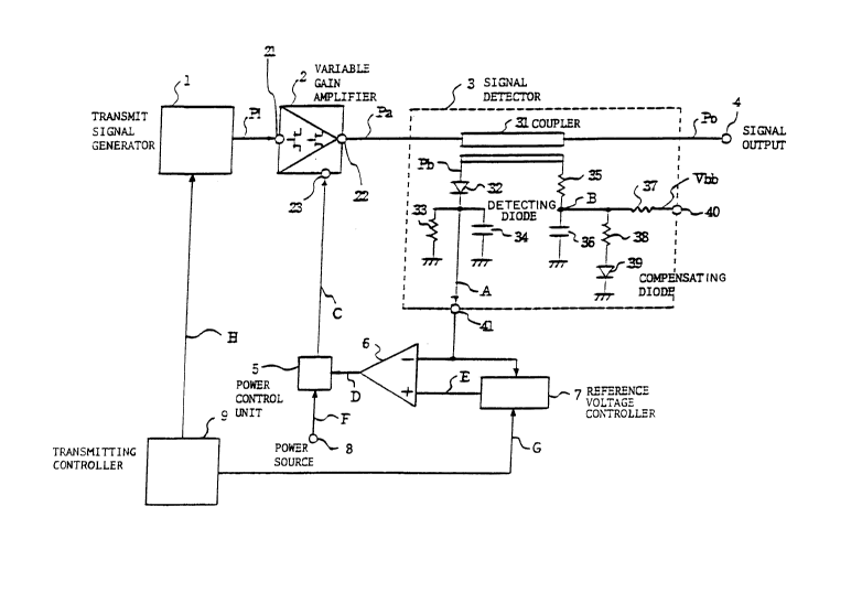
FIG. 1 ls a block dlagram showlng part of radlo-
fre~uency transmltter embodylng the present lnventlon;
,'f~ ' ~
~ 66446-545
20741 1 5
__ - 7 -
FIG. 2 is a waveform diagram showing waveforms
appearing at various points of the transmitter in FIG. 1,
wherein FIG. 2(a) shows the waveform of the transmit
output signal Po, FIG. 2(b) shows the waveform of the
output voltage A of the detectlng diode and FIG. 2(c)
shows the waveforms of the reference voltages E and G;
FIG. 3 is a circuit diagram showing a power control
unit 5 in the FIG. 1 transmitter; and
FIG. 4 is a block diagram showing an operational
amplifier 6 and a reference voltage controller 7 in the
FIG. 1 transmitter.
DETAILED DESCRIPTION OF THE PREFERRED EMBODIMENT
Referring to FIG. 1, a radio-frequency transmitter 100
intermittently outputs a transmitting output signal Po of
radio frequency. The transmitter 100 includes a
transmitting signal generator 1 which generates a burst
input signal Pi under the control of a transmitting
controller 9. The transmitter 100 also includes a
variable gain amplifier unit 2 which generates an
amplified signal Pa by amplifying the input signal Pi,
and a signal detector 3 which generates the transmitting
output signal Po by leading the most part of the amplified
signal Pa to a signal output terminal 4. The supply timing
of the input signal Pi is controlled by a transmission
control signal H from a transmission control unit 9. The
2074 1 1 5
_ - 8
signal detector 3 also supplies a part Pb of the amplified
signal Pa to a detecting diode 32 via a coupler 31, and
the detecting diode 32 generates across a load resistor 33
a signal detector output A which corresponds to the peak
level of the coupler output signal Pb, that is, the peak
level of the transmitting output signal Po. The signal
detector 3 further includes a compensating diode 39 with
substantially the same temperature characteristic as that
of the detecting diode 32. The detecting diode 32 and the
compensating diode 39 receive application of substantially
the same value of bias voltage, and are connected so as
to subtract the bias voltage variation in the compensating
diode 39 from the bias voltage variation in the detecting
diode 32 generated accompanying the temperature variation
in the forward voltage. Accordingly, the signal detector
output A that appears across the load resistor 33 includes
also a fixed bias voltage A0 with compensated temperature
variations along with a detected output corresponding to
the transmitting output signal Po.
The signal detector output A from the signal detector 3
is supplied to the inverting terminal of an operational
amplifier 6, and it is compared with a reference signal E
supplied to the non-inverting terminal of the operational
amplifier 6. A comparison output voltage D from the
operational amplifier 6 is supplied to a power control
unit 5. The power control unit 5 generates a control
2074 1 1 5
g
signal C from a source power voltage F of a source power
input terminal 8 in response to the comparison output
voltage D, namely, a voltage obtained by reducing the
source power voltage F in response to the magnitude of
the comparison output voltage D, and supplies the control
signal C to a control signal input terminal 23 of the
variable gain amplifier unit 2. In response to the control
signal C, the variable gain amplifier unit 2 controls the
source power voltage of the amplifier element, the drain
voltage of a field effect transistor (FET) here, and
- causes the amplification gain to be changed so as to
generate a predetermined transmitting output signal Po
at the signal output terminal 4 corresponding to the
reference voltage E.
-- The transmitting signal generator 1, the variable
gain amplifier unit 2, the signal detector 3, the power
control unit 5, the operational amplifier 6, and the
transmitting controller 9 have the same functions as in
the output level control circuit of the conventional
radio-frequency transmitter. On the other hand, the
output level control circuit according to this invention
further includes, besides the abo~e-mentioned various
components, a reference voltage controller 7 having a
bias voltage detecting circuit which stores the temperature-
compensated bias voltage A0 generated across the loadresistor 33 during the non-input period of the input
2074 1 1 5
-- 10 --
signal Pi and a reference voltage adding circuit which
superposes the stored bias voltage A0 on the input
reference voltage G. The reference voltage G iS supplied
from the transmitting controller 9 in synchronism with
the transmitting control signal H, and hence in synchronism
with the input signal Pi.
Referring simultaneously to FIG. 1 and FIG. 2, the
radio-frequency transmitter 100 is in the off-period of
the transmitting output signal Po for the duration from
the time T0 to the time Tl, and the reference voltage G
synchronized with the input signal Pi will not be supplied
either. During this period the detecting diode 32 does
not detect a coupler output signal Pb so that the output
voltage A of the diode 32 is substantially equal to the
fixed bias voltage A0. The fixed bias voltage A0 during
the off-period of the transmitting output signal Po is
stored in the bias voltage detecting circuit of the
reference voltage controller 7, and the stored bias
voltage A0 is supplied to the reference voltage adding
circuit of the controller 7. Since here the on/off period
of the input signal Pi coincides with the on/off period of
the reference voltage G, the reference voltage controller 7
determines the input time of the bias voltage A0 to be
stored by referring to the reference voltage G. At the
time Tl, the input signal Pi and the reference voltage G
are supplied from the transmitting signal generator 1 to
20741 1 5
-- 11 --
the variable gain amplifier unit 2 and from the transmitting
controller 9 to the reference voltage controller 7,
respectively. Since the transmitting output signal Po
is required to rise to a specified voltage within 2 milli-
seconds, the reference voltage G is raised according toa waveform in which the duration from the time Tl to
the time T3 is set to be less than 2 milliseconds. The
reference voltage controller 7 adds up the stored bias
voltage A0 and the reference voltage G to obtain the
reference voltage E for this output level control circuit.
- The reference voltage E is supplied to the inverting
terminal of the operational amplifier. During the period
from the time Tl to the time T3 the voltage A of the signal
detector output is lower than the reference voltage E, and
the gain control of the variable gain amplifier unit 2 by
the power control unit 5 is put in effect. As a result,
the power level of the transmitting output signal Po and
the signal detector output A of the detecting diode 32
quickly follow the change in the reference voltage E,
and at the time T3 the transmitting output signal Po
reaches a predetermined output corresponding to the
reference voltage G.
Moreover, if the input reference voltage G is supplied
directly to the operational amplifier 6 as in the prior art
(see FIG. 2(c)) instead of carrying out the above-mentioned
reference voltage processing using the bias voltage
20741 1 5
-
- 12 -
detecting circuit and the reference voltage adding circuit
of the reference voltage controller 7, the output voltage Al
of the detecting diode 32 (see FIG. 2(b)) rises delayed by
a time t from the reference voltage G, and correspondingly
the rise of a transmitting output signal Pol is also
delayed by the time t (see FIG. 2(a)). In the conventional
transmitting level control circuit, this time interval t
is as large as about 1 milliseconds, and it is difficult
to reduce the rise time of the transmitting output signal
Pol smaller than the specified rise time (2 milliseconds).
- Since, however, it is possible in this embodiment to make
the delay time t of the rise to zero, it is easy to reduce
the rise time (T3 - Tl) to within 2 milliseconds.
Furthermore, referring to FIG. 1, the power level of
maximum output of the transmitting output signal Po of
this radio-frequency transmitter is 0.6W, and it is possible
to carry out signal transmission by arbitrarily selecting
one of a plurality of output power levels that are separated
by an equal difference of 4 dB.
The variable gain amplifier unit 2 is an amplifier
including an FET as the amplifier element, which amplifies
the input signal Pi from a signal input terminal 21, and
outputs an amplified signal Pa from a signal output
terminal 22. The control signal C from the power control
unit 5 is inputted to a control signal input terminal 23
of the variable gain amplifier unit 2, controls the drain
2074 1 1 5
- 13 -
voltage of the FET, and controls the gain of the variable
gain a~plifier unit 2 by this drain voltage control.
Still further referring to FIG. 1, the signal detector 3
connects the coupling end of a signal coupler 31 to the
anode of the detecting diode 32, connects the cathode of
the diode 32 to a detecting voltage output terminal 41,
and outputs the signal detector output A through the
detecting voltage output terminal 41. The load resistor 33
and a capacitor 34 which forms a bypass circuit of the
radio-frequency signal are connected in parallel between
the cathode of the diode 32 and a grounding potential point.
In addition, the insulated terminal of the signal coupler 31
is connected to a series circuit of a terminal resistor 35
and a bypass capacitor 36 of the radio-frequency signal,
the series circuit terminating the amplified signal Pa.
A bias voltage Vbb is supplied from a bias voltage input
terminal 40, and the bias voltage Vbb gives a forward bias
voltage to the anode of the compensating diode 39 that has
its cathode grounded, via a series circuit of resistors
37 and 38. The junction of the resistors 37 and 38 is
commonly connected to the junction (point B) of the
resistors 35 and 36, and the bias voltage A0 which is
substantially equal to the bias voltage of the compensating
diode 39 is given also to the detecting diode 32. It
should be noted that the voltage of the bias voltage
supply point B is determined principally by the compensating
diode 39 and the circuit on the resistor 38 side.
2074 1 1 ~
- 14 -
When the amplified signal Pa is not inputted, the
load voltage that is produced at the detecting voltage
output terminal 41 or across the resistor 33, that is,
the bias voltage A0 of the diode 32, is lower than the
voltage at the common junction B (referred to as VB) by
the amount of the forward voltage Vf of the diode 32.
Since the forward voltage Vf of the diodes 32 and 39
changes accompanying temperature variations the voltage
at the point B which supplies the bias voltage to the
diodes 32 and 39 changes by the same amount of voltage
- in response to the variations in the forward voltage Vf.
Accordingly, the temperature variations in the forward
voltage Vf due to the diodes 32 and 39 cancel with each
other so that the voltage A0 generated at the detecting
voltage output terminal 41 essentially does not change.
Next, when the amplified signal Pa is applied to the
signal detector 3, the detecting diode 32 detects the
coupler output signal Pb, and generates the signal detector
output A which is the sum of the bias voltage A0 and the
detection output across the load resistor 33, that is,
at the detecting voltage output terminal 41.
Referring to FIG. 3, the power control unit 5 has a
transistor 51 to whose emitter a source power voltage F
from a source power input terminal 8 is applied. The
transistor 51 generates at its collector a control signal C
obtained by lowering the source power voltage F in response
20741 1 5
- 15 -
to its base current. In addition, a comparison output
voltage D from the operational amplifier 6 is supplied
to the base of a transistor 53, and the transistor 53
generates a collector current which corresponds to the
comparison output voltage D. The collector current of the
transistor 53 is supplied to the base of the transistor 51
via a resistor 52 to be served as the base current of
transistor 51. Since the voltage drop due to the
transistor 51 is decreased as the base current of the
transistor 51 is increased, the voltage of the control
signal C supplied to the drain terminal of the FET built
in the variable gain amplifier 2 is raised, increasing
the gain of the variable gain amplifier 2. Accordingly,
if the voltage of the signal detector output A is lower
than the reference voltage E, the comparison output
voltage D from the operational amplifier 6 is raised, and
the raise in the comparison output voltage D elevates the
gain of the variable gain amplifier unit 2. The increase
in the gain of the variable gain amplifier unit 2 causes
voltage of the signal detector output A to be raised
until it agrees with the reference voltage E.
Referring to FIG. 4, the reference voltage controller 7
carries out digital signal processing in response to the
analog signal detector output A from the signal detector 3
and the digital reference voltage G from the transmitting
controller 9, and the reference voltage E which is signal
20741 15
- 16 -
processed is supplied to the non-inverting terminal of
the operational amplifier 6. The signal detector output A
is converted to a digital signal by an analog to digital
(A/D) converter 72, and the obtained digital signal is
inputted to a controller (CONT) 73. This digital signal
is sampled by the controller 73 for every off period of
the reference voltage G. The sampled digital signal is
stored in a memory 75, and updated. The digital signal
stored in the memory 75 corresponds to the bias voltage AO
of the diode 32. On the other hand, the reference voltage
G is directly inputted to the controller 73. When the
reference voltage G is inputted, the controller 73 adds
the reference voltage G and the digital signal stored in
the memory 75, and supplies the added output to a digital
to analog (D/A) converter 71. The D/A converter 71
converts the added output to the analog reference voltage
E, and supplies the reference voltage E to the non-inverting
terminal of the operational amplifier 6.
It should be mentioned that when a high accuracy
setting of the bias voltage AO is not required, it is
unnecessary to update the digital signal for every off
period of the input of the reference voltage G, and may
be substituted by a preliminary storage in a read-only
memory 74 of the bias voltage AO obtained by an experiment
or the like.
Furthermore, the aforementioned operation may be
20741 1 5
-
- 17 -
replaced by the input of a transmission timing signal J
from the transmitting controller 9 to the controller 73
synchronized with the input-signal Pi, by storing in
advance the reference voltage G and the bias voltage A0
in the memory 74. The controller 73 reads the reference
voltage G and the bias voltage A0 from the memory 74
synchronized with the timing signal J to add these two
voltages, and supplies the added signal to the D/A
converter 71.
As described in the above, the output level control
- circuit of the radio-frequency transmitter according to
this invention can stably maintain the output power level
of the transmitting output signal Po over a wide range of
temperature by newly forming the reference voltage E
through addition of the bias voltage A0 of the detecting
diode 32 and the input reference voltage G, and controls
the output power level so as not to be left behind the
rise of the input reference voltage G. Moreover, the
above-mentioned output level control circuit does not
require the construction of a special control loop so
that the reduction of the number of circuit components
can also be accomplished.
Although the invention has been described with
reference to a specific embodiment, this description
is not meant to be construed in a limiting sense. Various
modifications of the disclosed embodiment, as well as other
20741 1 5
-
- 18 -
embodiments of the invention, will become apparent to
persons skilled in the art upon reference to the description
of the invention. It is therefore contemplated that the
appended claims will cover any modifications or.embodiments
as fall within the true scope of the invention.