Note: Descriptions are shown in the official language in which they were submitted.
2~7~8
M13T~IOD OF FORIIIN~ EL~3CTROD8S FOR T~E~NC~I CAPACITORS
FIBI,D OF T~ NVL_..ION
This invention relates to electrodes for trench
capacitor structures, and a method of forming electrodes of
a trench capacitor structure for an integrated circuit.
~ClC~ROUND OF TH13 I~VENTION
Trench capacitors with one or more polysilicon
electrodes for silicon integrated circuits may be fabri-
cated using known methods, and have applications in
structures such as DRAMS (Dynamic Random Access Memories)
and analog circuits. Typically, the number of masking
steps required depends on the number of polysilicon
electrodes. For example, in forming a simple trench capaci-
tor having one polysilicon electrode, in which the silicon
substrate acts as the other electrode, a conventional known
method includes steps of:
1. patterning and etching a trench in a silicon substrate;
2. formation of a capacitor dielectric on trench walls and
bottom, typically silicon dioxide;
3. filling of the trench with polysilicon by a known method
of chemical vapour deposition (CVD) to provide the
polysilicon electrode; and
. planarization by removal of the surface substantially
back to the level of the substrate surface.
The width of the trench polysilicon must be of
such a dimension to allow a contact to be made by a method
known in the industry. The resulting capacitor is formed
between a deposited top polysilicon electrode and the
silicon substrate. One masking step is required for
patterning and etching the trench. Depending on the method
of contact formation, another masking step may be required
for defining a contact area to the substrate.
A known method for providing a capacitor having
two polysilicon electrodes includes the steps of:
1. patterning and etching a trench in a silicon substrate;
2. forming an insulating dielectric layer on sidewalls and
a bottom of the trench;
': ' . , -' ' - - :
' ~ ' ' ' ' " ' . ' -
.. . - .. ~ :. . : . , .
~7Q~8
3. deposition and planarization of a first layer of poly-
silicon within the trench by a known method of CVD;
4. patterning and etching a second trench within the first
polysilicon layer to form sidewalls of the first poly-
silicon layer in the trench to serve as one of the
capacitor electrodes;
5. forming a layer of a capacitor dielectric on the etched
first polysilicon layer;
6. filling the resulting dielectric lined trench inside
the first polysilicon layer with a second polysilicon
layer by a known method of CVD; and
7. planarization of the second polysilicon level with the
substrate and first polysilicon surfaces.
Thus, a first ~k;ng step is required for de-
fining the trench in the substrate (step 1) and a second
masking step is required (step 4) for defining a second
trench within the first polysilicon layer. The width of
the second polysilicon within the second trench must be
such as to allow a contact to be made by methods known in
the industry. Depending on the method of contact forma-
tion, another masking step may be required for formation of
a contact to the second polysilicon layer. Hence a ~ n;
of two masking steps are required for formation of a trench
linear capacitor with two polysilicon electrodes, one each
for the trench and at least one polysilicon electrode.
~U~ARY OF T~ INV~NTION
The present invention seeks to provide electrodes
for a trench capacitor structure for an integrated circuit
and a method of forming electrodes for a trench capacitor
structure in which the nl ~- of -ck; ng stepg is reduced.
Thus, according to the present invention there is
provided a method of forming electrodes of a trench capaci-
tor structure for an integrated circuit, comprising:
providing a sub~trate having a planar surface and defining
therein a trench, the trench having sidew?lls and a bottom;
providing a conformal first dielectric layer extending over
sidewalls and bottom of the trench; providing a conformal
. _, .. ~ , . . .
,
2 ~ 7 ~
first conductive layer overlying the first dielectric layer
within the trench; providing a conformal second dielec~ric
layer overlying the first conductive layer within the
trench; providing an overlying conformal second conductive
5 layer within the trench; and planarizing the resulting
structure by removal of each of said dielectric layers and
conductive layers extending above the planar surface of the
substrate, to expose substantially coplanar surfaces of
each layer within the trench.
lo Thus the present invention provides a method of
forming a plurality of trench isolated electrodes of a
capacitor structure for an integrated circuit which
requires only one mask level for engraving ~he trench. Two
or more self-aligned electrodes are formed from conformal
layers of conductive material and dielectric material
within the trench. Since each layer is conformal and thus
effectively self-aligned within the trench, successive
layers conform to the contour of the trench defining the
first layer, and photomasking steps for defining each
; 20 conductive layer are not required. After filling of the
trench with a selected number of conformal conductive
layers and intervening conformal dielectric layers, a
; single planarization step removes each layer extending
above the substrate surface. Thus contact areas to each
conductive layer are exposed level with the ~urface of the
substrate .
Advantageously, in forming a capacitor structure
having two electrodes, the trench has a first, wide portion
and a narrow portion of smaller lateral dimension, and the
step of providing a first conductive layer fills the narrow
portion of the trench and leaves a cavity within the first
portion of the trench. The second dielectric layer and the
second conductive layer fill the cavity within the first
portion of the trench. Thus two differently filled regions
of the trench are provided, the narrow portion of the
trench providing a contact area for the first conductive
layer which forms a lower electrode, and the wider portion
, ,: . .
- . . ..
:,
,
2~7~8
g
of the trench filled with subsequent layers of dielectric
and conductive layers. After planarization, the exposed
surface of the first conductive layer in the narrow portion
of the trench has a lateral width of twice the thickness of
the first conductive layer, sufficiently large for forma-
tion thereon of a contact, and similarly, a contact area to
the second conductive layer is provided in the wide portion
of the trench. Hence formation of first and second elec-
trodes for a trench linear capacitor is achieved in a
lo maskless process sequence. Furthermore, a resulting
structure which has substantially coplanar contact areas
simplifies the formation of contacts to each electrode by a
conventional known method.
Preferably, the planar surface of the substrate
comprises a protective layer of chemical-mechanical polish
(CMP)resistant material and the step of planarizing
comprises chemical-mechanical polishing to provide a fully
planarized topography, although other suitable planariza-
tion methods may be used. Consequently, coplanar contact
20 areas are provided to each conductive layer, and topography
related problems are reduced in subsequent processing
steps.
According to another aspect of the present
invention there is provided a method of forming trench
isolated electrodes of a capacitor structure for an
integrated circuit, comprising: providing a substrate
having a planar surface defining therein a trench having
sidewalls and a bottom, the trench having a first portion
and a narrower portion of smaller lateral dimension: pro-
viding a conformal layer of dielectric material over side-
walls and the bottom of the trench, the dielectric layer
leaving a cavity within the trench; providing a conformal
layer of a conductive material overlying the dielectric
layer the thickness of the conductive layer being
3s sufficient to completely fill narrow portions of the trench
and a part of said cavity ,~ ~i n 1 ng unfilled in the first
portion of the trench; filling the trench by providing
. ,
- . ' . ,
-
2~7~4~
within the trench subsequent conformal layers comprising at
least an other conformal dielectric layer and an overlying
conformal conductive layer; and planarizing the resulting
structure by removal of material of the dielectric layer
5 and of the conductive layer and subsequent conformal layers
extending above the planar surface of the substrate to
expose surfaces of each of said layers within the trench
substantially coplanar with the substrate surface whereby
each conductive layer forms one of a plurality of trench
lo isolated electrodes.
Thus, in forming a capacitor having a plurality of
electrodes, after providing a second dielectric layer and a
second conductive layer which partially fills the cavity
within the first portion of the trench and before planariz-
ing the resulting structure, another conformal layer ofdielectric and another conformal layer of conductive
material is provided, thereby filling the cavity within
the trench and forming a third trench isolated electrode.
Thus multiple electrodes may be provided within the trench
without additional masking steps, each subsequent conformal
layer of conductive material forming an electrode aligned
within the cavity defined by the underlying conformal
layers.
According to another aspect of the present
invention there is provided a method of forming electrodes
of a trench linear capacitor for an integrated circuit
comprising: providing a substrate having a planar surface
and defining therein a trench having sidewalls and a
bottom, the trench having a first portion and a narrow
portion of smaller lateral dimension; providing a conformal
fir8t dielectric layer extending over sidewalls and the
bottom of the trench; providing a conformal first con-
ductive layer overlying the first dielectric layer, the
first conductive layer being sufficiently thick so that the
narrow portion of the trench is completely filled with the
first conductive layer, and part of said cavity "-. in~ in
the first portion of the trench; providing a conformal
- : ., . , , . . : -
- , - . . . . - , .
' ' ' ' - ' . ', .. . ,, ' ' , , .
-. . : . .. ., , ~ . - . ~ . -
.... . . . :. .. ~ . .
2074~8
second dielectric layer overlying the first conductive
layer in said cavity; providing a conformal second con-
ductive layer over the second dielectric layer, the second
conductive layer being sufficiently thick to fill said
5 cavity r~ ~ln;ng in the trench; and planarizing the result-
ing structure by removal of layers extending above the
planar surface of the substrate, to expose substantially
coplanar surfaces of the first and second conductive
layers, the first and second conductive layers thereby
lo providing trench isolated first and second electrodes, and
the exposed surfaces of the second conductive layer in the
first portion of the trench and of the first conductive
layer in the narrow portion of the trench thereby providing
planarized areas sufficiently large for defining electrical
contacts thereon.
Thus, in forming of a trench linear capacitor
structure with two conductive electrodes, neither of which
are the semiconductor substrate, the requirement for a
masking step to define the electrode structures is avoided
and regions for contacting both conductive electrodes are
provided also without the use of a ~ck; ng step. A single
photoengraving (i.e. photolithographic) step is required
only for defining the area for etching the trench.
Advantageously, a protective layer is provided on
the substrate surface to allow for removing surface layers,
preferably by chemical-mechanical polishing, to provide a
fully planarized surface with coplanar areas exposed on
each conductive layer for formation of first and second
electrode contacts.
According to a further aspect of the present
invention there is provided a trench capacitor structure
for an integrated circuit, comprising: a ~ubstrate having
a planar surface and defining therein a trench region, the
trench region having sidew~11~ and a bottom, the trench
region being filled with a plurality of conformal layers
comprising: a conformal first dielectric layer extending
over sidewalls and bottom of the trench; a conformal first
, . . . . ~ . ~ , . - : , . ............... - . . ~
- . . , , ,: : . .; - - -
,. ,. . ,. ~ . , , -
- :. . : ,- - , , - . . .
2~7~8
conductive layer overlying the first conformal dielectric
layer, and at least an other conformal dielectric layer
overlying the first conductive layer and an overlying
conformal conductive layer within the trench; and each of
the conductive layers and the dielectric layers having
planarized surface areas substantially coplanar with the
substrate surface, the planarized surface area of each of
the conductive layers being sufficiently large for forma-
tion thereon of an electrical contact, the conductive
lo layers thereby forming electrodes isolated from one another
within the trench region by a dielectric layer there-
between.
According to yet another aspect of the present
invention there is provided a trench linear capacitor
structure for an integrated circuit, comprising: a
substrate having a planar surface and defining therein a
trench region, the trench region having sidewalls and a
bottom, the trench region being filled with layers com-
prising: a conformal first dielectric layer extending over
sidewalls and bottom of the trench; a conformal first
conductive layer overlying the first conformal dielectric
layer; a second conformal dielectric layer overlying th~
first conductive layer, and an overlying second conformal
conductive layer; and the first and second conductive
layers and the first and second dielectric layers each
having planari~ed surfaces substantially coplanar with the
substrate surface, the planarized surface areas of each of
the first and second conductive layers being sufficiently
large for formation thereon of an electrical contact, the
first and second conductive layers thereby forming first
and second electrodes isolated from one another within the
trench region by the second dielectric layer therebetween.
Preferably, in a linear trench capacitor structure
having two electrodes, the trench region comprises a first,
wider portion and a narrow portion of smaller lateral
dimension, the narrow portion of the trench region is
filled by layers comprising the first dielectric layer and
~.: . ~, -. .. ... -......... . . :: . . ,.- .. : ,
.' . '' '' '"' ~'-, ' , ' , :' ' .
- . -
., . . - . . ..
-: . : . - ,
2~7~3
first conductive layer only, and the wider first portion of
the trench is filled also with the second conductive layer
and the underlying first dielectric layer. Thus the two
portions of the trench are differently filled and the
planarized surfaces provide sufficiently large coplanar
contact areas for contacts to the first and second elec-
trodes by a conventional known method. Conveniently, a
contact to the first electrode is made in the narrow region
of the trench and a contact area to the second electrode is
lo made in the first portion of the trench. ':
Thus, the present invention provides a method of
forming trench isolated electrodes of a capacitor structure
for an integrated circuit, a method of forming electrodes
of a trench linear capacitor, a capacitor structure, and a
trench linear capacitor structure using a reduced number of
photoengraving or masking steps.
E~RIEF DB8CRIPq!ION OF T~3 DRAWING~
Embodiments of the invention will now be described
by way of example, with reference to the accompanying
drawings, in which:
~ Figure 1 shows schematically a known prior art
polysilicon-to-substrate silicon trench capacitor for a
DRAM;
: Figure 2 shows schematically a known prior art
2s structure of a polysilicon-to-polysilicon trench capacitor
for a DRAM;
Figure 3 shows a structure in plan view; Figures
: 3A and 3B show respectively first and second cross-
sectional views, at a process step in a method of forming a
trench linear capacitor according to a first embodiment of
the invention;
Figures 4 to 7 show the structure as in Figure 3
in plan view: in Figures 4A to 7A a first cross-sectional
view; and in Figures 4B to 7B a second cross-sectional view
at progressive steps in a method of forming a trench linear
capacitor according to the first embodiment; Figure 7C
shows a cross-sectional perspective view of the resulting
- .. :. . . . : ... ..
-.
. . . , - . : .
, : ., , - : . :
.. ~ .
" . . . . - , ~ ,
-
. -,-: . . - . , .
2~7~
structure shown in Figures 7, 7A and 7B;
Figure 8 shows a capacitor divider structure
according to a second embodiment of the invention in plan
view; Figures 8A and 8B cross-sectional views; and Figure
5 8C shows an equivalent circuit diagram; and
Figure 9 shows a plan view and Figures 9A, 9B and
9C show respectively first, second and third cross-
sectional views respectively of a capacitor structure
according to a third embodiment of the present invention;
lo and Figure 9D an equivalent circuit diagram comprising a
biased or grounded isolation capacitor structure; and
Figure 9E an equivalent circuit diagram comprising a
reading or writing electrode for a memory capacitor, as
representative applications of the structure according to a
third embodiment of the present invention.
D138CRIPTION OF THE~ PR~3F13RR13D l~MBODIN2NTS
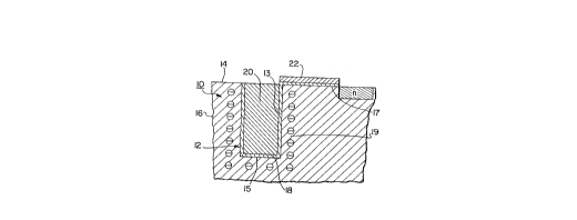
A trench capacitor 10 of known prior art structure
is shown in Figure 1, and comprises a trench 12 defined
within a surface 14 of a part of a semiconductor silicon
wafer 16 which forms a substrate for an integrated circuit.
The trench 12 is formed by selectively masking the surface
14 by a known method, for example, by coating with photo-
resist and patterning, and then etching a trench 12 by a
known method, typically anisotropic reactive ion etching.
The resulting trench 12 has steep sidewalls 13. A di-
electric layer 18, typically of silicon dioxide, is grown
or deposited within the trench 12 so as to extend con-
formally over the sidewalls 13 and bottom 15 of the trench
and over the surface 17 adjacent the trench. A conformal,
conductive layer of polysilicon 20 is provided by chemical
vapour deposition to fill the L~ ~;n;ng volume of the
trench to form the top electrode of the charge storage
capacitor. The silicon substrate acts as the bottom
capacitor electrode, and forms the memory charge storage
node. A second layer of conductive polysilicon is
deposited to extend over the surface 17 adjacent the trench
and is patterned to define a top electrode 22 adjacent the
.
,; ~ -
2~7~
trench. The top electrode 22 electrically connects the N+
diffusion to the substrate capacitor electrode for the
purposes of pumping charge for storage according to the
wordline potential. Therefore, ln the trench to substrate
5 capacitor so formed, stored charge is located as indicated
schematically in Figure 1, at the silicon substrate surface
region 19 surrounding the trench 12.
A trench linear capacitor 30 of known structure,
having two electrodes 40 and 50, buried inside a trench 32
lo and isolated from the substrate 36 is shown in Figure 2.
In a known method of forming a capacitor of this structure,
a steep-sided trench 32 is provided within the surface 34
of the substrate 36 silicon wafer by a known method of
anisotropic ion etching. A first dielectric layer 38 is
grown or deposited to line the trench 32 and then a first
conductive layer 40 of a conductive material, i.e. doped
polysilicon, is deposited overall on the wafer to fill the
entire trench. After planarization and removal of excess
polysilicon extending over the surface 34, the L~- -in;ng
20 first polysilicon layer 40 is contained within the trench
32, which is completely filled, and the exposed surface of
the polysilicon layer 40 is planar with the silicon surface
34. A second trench is defined by photoengraving, i.e. by
coating with photo-resist, patterning photo
lithographically, and then etching the second trench within
the first polysilicon layer 40, thereby removing the centre
region of the first polysilicon, so that only the sidewalls
40 of the original first polysilicon layer r- ~l n in the
trench 32. These sidewalls 40 form the bottom electrode of
the trench capacitor. A second dielectric layer 42 is
grown or deposited over the sidewalls 40 and the bottom 33
of the original trench 32. A second conductive polysilicon ''
layer 50 is deposited to completely fill the trench inside
the first polysilicon layer and also to coat the entire
surface 34 of the substrate 30. After planarization and
removal of the excess second layer polysilicon over the
surface 39, the structure shown in Figure 2 is formed.
. - . . . -- . , , - .. . . . . .
.- , - . . - . . . . ~ - -
. . . ... . . . ., -. . , :
.: . . ., -:. , . .. - - : ~ -:.
- . . . . ...
2~7~8~8
11
Thus, the trench 32 is fllled with layers forming the first
dielectric 38, bottom polysilicon electrode 40, second
dielectric 42 and top polysilicon electrode 50. Electrode
40 forms the storage node of the capacitor. In this
5 process, at least one of the linear capacitor electrodes 40
and 50, as well as the trench, must be defined photo-
lithographically.
In a method of forming a trench linear capacitor
structure 55 (Figure 7C) for an integrated circuit
lo according to a first embodiment of the present invention,
as shown schematically in each part of Figures 3 to 7,
which shows part of a silicon wafer 60 forming a substrate
for an integrated circuit. A coating of a first masking
layer 62, comprising for example silicon nitride, is
lS deposited to serve as a chemical-mechanical polish stop
layer, as will be described below. Then, a coating of a
second masking layer 64, for example silicon dioxide, is
grown or deposited thereon to serve as a trench etch mask.
The two masking layers 62 and 64 are patterned photo-
lithographically and engraved as shown in Figure 3b by amethod known in the industry, so as to expose a selected
area 66 of the underlying surface of the substrate 60 for
defining and etching a trench 70. As shown in Figure 3,
from the top plan view of the area 66, the trench 70 has a
2s first wider portion 72 ànd a second relatively narrow
portion 74. The lateral dimensions of the wider portion 72
and naLlo.~er portion 74 are parameters which influence the
c~p~c;tance of the resulting trench capacitor 55.
The selected area 66 of the substrate 60 is
etched by an anisotropic etching process known in the
industry, to a predetermined depth to form a deep, steep-
sided trench 70. As an example, a trench may be provided
by a known anisotropic etch comprising reactive ion etching
of the silicon wafer substrate in a plasma generated from
CBrF3. The length and depth of the trench is selected
according to the capacitance value required. The lateral
dimension or width of the trench is wide enough to
., ~ . ... . . . . . .
: . . . .
.. . . ..: .. ~
,- .
2~7~ 8
12
accommodate the selected thicknesses of each of the di-
electric and conductive layers to be deposited in the
trench, and in the example described below, the width of
the first port~on 72 is 3.5~m and the width of the narrower
5 portion 74 is 1.5~m (Figure 4).
After formation of a steep-sided trench 70, the
trench is cleaned in an HF solution which simultaneously
removes the r~m~;n;ng trench etch mask layer of silicon
dioxide 64, leaving only the layer 62 of silicon nitride
lo exposed on the wafer surface all around the trench. A
layer of a first dielectric 78 of, for example, ~400nm
thickness of silicon dioxide is grown or deposited con-
formally overall so that the layer 78 of dielectric lines
the sidewalls 73 and bottom 75 of the trench 70 and extends
over the planar surface of the nitride layer 62 around the
trench. A first conductive layer 82, for example, of a
layer of conductive polysilicon is then deposited con-
formally over the substrate by an LPCVD (low pressure CVD)
method known in the industry. The thickness of the poly-
silicon layer 82 is selected so that it completely fillsthe narrower portion 74 of the trench 70, as shown in cross-
section in Figure 5A, and the wider portion 72 of the
trench remains partially unfilled, leaving a cavity 71 as
shown in Figure 5B. In this example, the conductive layer
82 is 350nm thick, phosphorus or boron doped polysilicon,
as is typically used in the indu~try. The conductive layer
82 of polysilicon is, for example, formed by a conventional
method of polysilicon CVD with in situ doping.
After deposition of the first polysilicon layer
82, a second dielectric layer 88, is grown or deposited
conformally overall (Figure 6). The second dielectric 88,
composed of one or more electrically insulating materials
forms the capacitor dielectric, and by way of example, is
30nm of silicon dioxide thermally grown at 950~C by a known
method. A second conductive layer 90, for example, of
doped polysilicon, is deposited conformally over the di-
electric layer 88. The thickness of the second conductive
- .- . . - . .
- - , . . . .~ , . . . .
. .: . - .
~ -: , : . . . : -
2 ~ 8
13
layer is such that it completely fills the r~m~;n;ng cavity
in the wider portion 72 of the trench 70. The conformal
polysilicon layer 90 may leave a depression 92 near the
centre of the trench 70. The contour of this depression is
dependent on the deposition thickness and trench width.
Thus the narrower portion 72 is filled by the first di-
electric layer and the first conductive layer only (Figure
6A). The wider first portion 72 of the trench is filled by
the dielectric layers 78 and 88 and conductive layers 82
o and 90 (Figure 6s). In this example, the wider portion 72
of the trench has a lateral dimension of twice the sum of
the combined thicknesses of the conductive polysilicon and
oxide dielectric layers and the narrow portion is not wider
than twice the combined thicknesses of the first poly-
silicon and first dielectric layers. The first and second
dielectric layers isolate the first and second conductive
electrodes within the trench, each of these layers 78, 88,
82 and 90 extending over the planar surface of the silicon
nitride layer 62 on the substrate 60 around the trench 70.
The resulting structure is then planarized by
removing material of each of the layers of 90, 88, 82 and
78, extending above the planar surface of the protective
! layer 62 of silicon nitride (Figure 7). Thus coplanar
surfaces of each of the dielectric and conductive layers
90, 88, 82 and 78 are exposed substantially coplanar with
the silicon nitride surface layer (Figures 7A and 7B). The
first conductive polysilicon layer 82 forms the bottom
electrode of the linear capacitor 55 (Figure 7C). The
narrow portion of the trench is completely filled with the
first layer of polysilicon and provides a region having asurface cross-sectional area 97 large enough for defining
thereon a contact to the bottom electrode 82. An area 95
for formation of a contact to the top electrode is provided
on the exposed surface of the second polysilicon layer 90
35 (Figure 7C) in the first region 72 of the trench. -
A preferred method of planarization is removal of
the surface layers by chemical-mechanical polish;ng, for
.
.
.
- , . . .
~7~g~
example using a commercially available chemical-mechanical
polishing solution of a silicon based slurry which
selectively removes polysilicon layers 82 and 90 and
silicon dioxide layers 78 and 88 relative to the masking
layer of silicon nitride 62. The latter provides a rela-
tively hard, etch resistant protective layer which
functions as an etch stop. The resulting surface is thus
fully planarized back to the level of the surface of the
thin layer of silicon nitride (Figure 7).
lo A top view of the resulting structure is shown in
Figure 7A. The wider portion of the trench has a central
area of conductive material 90 which forms the top
electrode of the linear capacitor 55. In the plan view of
Figure 7, the top electrode 90 is surrounded by a ring of
dielectric material of layer 88, forming the capacitor
dielectric, and a ring of conductive material of layer 82
forms the bottom electrode of the capacitor. The layer 82
is separated from the substrate 60 by dielectric layer 78.
The narrower portion 74 of the trench contains an area of
conductive material of layer 82 only, separated from the
substrate by dielectric layer 78. Figures 7, 7A and 7B
show a top view and cross-sectional views of the resulting
structure including regions 99 of the conductive layers,
for contacting the top and bottom electrodes. Electrical
contacts to coplanar regions 99 are formed in subsequent
processing steps by a known conventional method.
Thus the method provides for formation of two
electrodes of a trench linear capacitor without the need
for a photolithographic mask. Each electrode is formed
from a conformal layer of polysilicon isolated by conformal
layers of dielectric. Each conformal layer is thus
effectively self-aligned within the trench region and
masking steps for each electrode are not required. The
trench isolated electrodes are formed in a maskless process
and the number of processing steps is reduced. Advan-
tageously, coplanar areas for formation of contacts to each
electrode are provided on a level planar with the surface
:. : . . . . ...................... . . .
- . : , , : : . ~, . - .
. - . , . . . - - - . .
~ 15 2~7~ 8
of the substrate and a single planarization step is used to
planarize each of the conductive and dielectric layers.
Subsequent processing steps in small geometry, i.e. 0.5~m,
device processes are simplified by the fully planarized
s topography.
The method according to the emhodiment is com-
patible with bipolar and MOS processes which utilize trench
isolation in CMOS and BiCMOS technologies.
A capacitor divider structure 120 according to a
o second embodiment of the invention is shown in Figure 8.
Similar reference numerals incremented by 100 are used in
Figure 8 as in Figures 3 to 7 to denote corresponding
elements of the structures of the first and second embodi-
ments. In plan view, Figure 8, the capacitor divider
structure 120 comprises two similar wider portions 171 and
172. Thus the capacitor structure of the second embodiment
is similar in structure to two similar simple capacitor
structures of the first embodiment joined through the
narrow portion 174 extending between the two wider portions
171 and 172. The cross-sectional structures of the wider
portion 171 and narrow portion 174 are shown in Figures 8A
and 8B and are similar to the first and second cross-
sections of the capacitor of the first embodiment (Figures
7A and 7s). It will be clear from the similarity of
elements of the capacitor structures of the first and
second embodiments, that after defining a suitably shaped
trench having wide portions 171 and 172 connected by a
narrow portion 174, the capacitor divider structure
according to the second embodiment is fabricated by a
similar se~uence of process steps as the capacitor of the
first embodiment. The trench 170 is filled with a confor-
mal first dielectric layer 178, a conformal first con-
ductive polysilicon layer 182, filling the narrow portion
and leaving a cavity in each of the wider portions 171 and
172 of the trench. A conformal second dielectric 188 and a
conformal second polysilicon layer 190 are then provided in
the remaining cavities to form an isolated electrode in
' .'' ' ' ' . ~ ' . '
,
,
2~7~8
16
each wide portion 171 and 172 of the trench 170. Thus a
three electrode structure is formed by a maskless process.
A biased or grounded isolation electrode structure
130 according to a third embodiment of the present inven-
5 tion is shown in plan view in Figure 9 and in cross-section
in Figures 9A and 9B. As shown in Figure 9d, the structure
comprises three electrodes. In a method of fabricating the
structure, a trench 270 is defined which, as shown in plan
view in Figure 9, has a stepped structure comprising a
narrow portion 274, an intermediate width portion 273 and a
wide portion 272. In cross-section through narrow and
wider portions 274 and 273, (Figures 9A and 9B
respectively) the structure is similar to that of the
narrow portion 74 and wide portion 72 respectively of the
capacitor structure according to the first embodiment
(Figures 7A and 7B). The structure 130 is provided by a
similar sequence of processing steps to the first and
second embodiments: after photoengraving and etching the
; stepped trench, conformal layers of a first dielectric 278,
first conductive layer 282, second dielectric 288 and
second conductive layer 292 are provided, as described
above, except that the second conductive layer does not
fill the trench 270. After deposition of the second
conductive layer 290, a cavity remains in the wide portion
272 of the trench. A conformal layer of thin third di-
electric 29~ is then deposited to line the remaining cavity
in the wide portion 272 of the trench, and a conformal
third conductive layer, i.e. another layer of conductive
polysilicon 292 is deposited to fill the wide portion 272
of the trench. After planarization of the resulting
structure by a known method, such as chemical-mechanical
polishing as described in the first embodiment, the cross-
section through the wide portion 272 is as shown in Figure
9C. The resulting structure may function, for example, as
an isolation electrode, e.g. as in an equivalent circuit as
illustrated in Figure 9D, or as a reading or writing
electrode for a memory capacitor (RAM, ROM, EPROM) as
. . . . . - . . . - . .: . ... .
.. .. ,,
. . . . . - . ,
- . ~ - : :
.
2Q7~
17
represented in Figure 9E. Thus a three electrode capacitor
structure is provided by a maskless process, a photo-
lithographic process step being required only for defining
the trench.
It will be apparent from the embodiments described
that other trench structures having a plurality of elec-
trodes for capacitors and other integrated circuit devices
may be provided within the scope of the invention by
modifying or varying the process steps of the embodiments.
Since each layer filling the trench is conformal, each
electrode and each inter-electrode dielectric layer is in
effect self-aligned within the trench, and the structure of
each electrode is dependent on the geometry of the trench.
Photo-lithographic steps are not required to define each
electrode, and consequently a single planarization step
only is required after filling the trench with a plurality
of conductive and dielectric layers. The number of mask
levels used for complex analog BiCMos process can be
reduced. Furthermore, the process allows for formation of
a capacitor at the initial stages of processing, while
ret~;n;ng wafer planarity.
In modifications of the embodiments of the inven-
tion, the dielectric layer of silicon dioxide is formed
compositely by thermal oxidation following deposition.
Alternatively, other known insulating materials are used
instead of CVD silicon dioxide, for example, a layer of
silicon nitride or silicon oxynitride formed by a known
method of oxidation, thermal oxidation or an ONO (oxy-
nitride oxide) process; or a metal oxide such as tantalum
3 o pentoxide
Conductive polysilicon is provided alternatively
by deposition of polysilicon followed by ion implantation
of dopant to provide conductive polysilicon of a desired
resistivity. Alternative conductive materials which may be
used to form electrodes include metals which may be
deposited to form a conformal layer, for example CVD
tungsten. In the latter example a suitable dielectric
', ', ' ~. ~',', -
- - ,
2 ~
18
layer may be provided by high pressure oxidation of
tungsten to form tungsten oxide.
The chemical-mechanical polish stop layer alterna-
tively comprises other hard polish resistant materials, for
5 example, silicon carbide. Since the polish stop material
must be more polish resistant than the conductive or insula-
ting layers, silicon carbide is advantageous when the
conductive material is a hard metal, for example, tungsten.
Other conventional etch back methods for planar-
ization, for example, reactive ion etching may be used.However, planarization by chemical-mechanical polishing is
particularly advantageous in providing a fully planarized
~ surface topography. Coplanar contact to two or more
electrodes can then be made thus simplifying subsequent
process steps and reducing topography related photo-
engraving and etch problems in defining conductive inter-
connect structures, particulary for deep submicron (i.e.<
O.5~m) technology.
. .
- . .
' ~ ~ ' .. ', ' .. :'
''
,' ~ ,
, ' - . ', '- .: ', ' ~ '~
, . - .