Note: Descriptions are shown in the official language in which they were submitted.
~ UK9-91-0~4
2 ~ 2
NON-LINEAR INDUCTOR WITH ~AGNETIC FIELD REDUCTION
The present invention generally relates to a non-linear
inductor with magnetic field reduction for use in a
raster-scanned CRT display such as a television receiver or
a computer visual display unit.
.,
A raster-scanned CRT display comprises a line timebase
circuit or generating a sawtooth deflection current in a
pair of el~ctromagnetic line scan coils. The deflection
current energises the coils to produce a time variant
magnetic deflection field. The deflection field scans one or
more electron beams from one side of the CRT screen to the
other side during a line scan period and rapidly returns the
electron beam durin~ a retrace or flyback period to the
start of the next line of -the raster to be scanned. The line
timebase circuit typically comprises an inductor connected
in series with a high volta~e solid state switch such as a
bipolar transistor. During the line scan period, the switch
is closed and current flows through the inductor and switch
from a high voltage DC supply (typically lOOV) to ground.
The current flowing through the inductor and the current
10wing in the scan coils increase at a rate proportional to
the voltage across the inductor. During the flyback period,
the switch is opened. The current in the inductor rapidly
reverses and a back Electromotive Force (EMF) or "flyback
pulse" is generated across the inductor by the collapsing
magnetic field in the inductor. The 1yback pulse is
controlled by a tuning capacitor connected across the
switch. The back EMF dissipates causing the current in the
scan coils to rapidly reverse. The electron beam is thus
deflected rapidly back to the start of the next scan line.
Ideally, the de1ection coils would be pure
inductances. In practise however, the coils have a DC
resistance. The resistance causes an asymmetric
non-llnearity in the sawtooth deflection current. The
non-linearity gives rise to objectionable asymmetric
distortion of an image displayed on the CRT screen. The
asymmetric distortion is a function of the inductance to
UK9-gl-044 2
resis-tance ratio of the deflection coils and therefore
varies proportionally with frequency.
In a typical CRT display, the asymmetric non-linearity
is corrected by connecting a non-linear inductor in series
with the deflection coils. The non-linear inductor typically
comprises a permanent magnet posikioned adjacent an
inductive winding. The inductance of -the non-linear inductor
varies about an operating point as a function of the current
flowing through the winding. Some non-linear inductors
comprise a moveable magnet which can be set in position
during a manufacturing process step. The moveable magnet
permits manual adjustment of the polarity of the magnet
relative to the winding, and therefore changes the operating
point of the inductor. In a colour CRT display, low level
magnetic correction fields are arranged around the neck of
the CRT to optimise electron beam convergence and colour
purity. The magnetic field from the magnet can interfere
with these correction fields and thus degrade picture
quality. To minimise such degradation, the non-linear
inductor i8 usually located as far away from the CRT as
possible. However, because CRT displays are becoming smaller
in size, and CRT resolution is increasing, it is becoming
increasingly difficult to prevent the stray field from the
non linear inductor from interfering with the correction
fialds.
Such interference may be prevented by magnetically
screening the non linear inductor from the CRT. However,
this is both costly and space consuming. Alternatively, as
described later with reference to Figure 7 of the
accompanying drawings, another magnet may be located on in
the vicinity of the non linear inductor to deflect the
magnetic field from the non linear inductor away from the
CRT. However, the deflection provided by the other magnet is
very sensitive to its position relative to the CRT and the
non linear inductor. Therefore, printed circuit board space
must be set aside for accommodating the other magnet.
~ UK9-91-0~ 3 2~ 9~
In accordance with -the present invention, there is now
provided a non-linear inductor comprisiny: a bobbin carrying
an inductive coil; a first permanent magnet adjacent the
coil; and a second permanen-t magnet positioned and oriented
relative to the first magnet in such a manner that the
magnetic field generated by the non-linear inductor is
substantially reduced.
Because the second magnet is oriented to substantially
cancel the magnetic fiel~" no additional maynets are
re~uired for deflecting the magnet fielcl away from the CRT.
'.
Viewing the present invention from a second aspect,
there is provided a non-linear inductor comprising: a bobbin
carrying an inductive coil; a first permanent maynet
ad~acent the coil; and a second permanent magnet positioned
and oriented relative to the first magnet in such a manner
that the magnetic field generated by the first magnet is
opposed to the magnetic field generated by the second
magnet.
,.............................................................. .
Because the second magnet is integral, a non linear
inductor of the present invention occupies the same printed
circuit board area as a conventional non linear inductor.
.,
A preferred embodiment of the present invention will
now be described, by way of example only, with reference to
the accompanying drawings in which:
Figure 1 is a circuit diagram of a line timebase
circuit for a CRT display of the prior art.
Figure 2 is a waveform diagram corresponding to the
line timebase circuit shown in Figure 1.
Figure 3 is a waveform diagram illustrating a
non-linear deflection current and a corresponding image
geometry distortion.
UK9-91-044 4
2~7~.9,~
Figure * ls an isome-tric view of a non linear inductor
of the prior art.
Figure 5 is a graph illustrating the induc-tance of the
non-linear inductor varying as a function of current flowing
through the non-linear inductor.
Figure 6 is a waveform diagram illustrating the
inductance of the non-linear inductor varying as a unction
of a sawtooth deflection current flowing through the
non-linear inductor.
Figure 7 is an isometric view of conventional apparatus
for deflecting the magnetic field generated by the non
linear inductor shown in Figure 4 away from a CRT.
Figure 8 is an isometric view of a non-linear inductor
of the present invention.
Figure 1 shows an example of line timebase or "flyback"
circuit comprising an inductor 10 connected between a high
voltage (lOOV) supply rail ~ and the collector of a bipolar
transistor switch 11. The emitter of transistor 11 is
connected to ground. A capaci-tor 12 is connected between the
collector of transistor 11 and ground and a diode 13 is
connected across capacitor 12 for conducting current from
ground to the collector of transistor 11. A pair of line
deflection coils 14 are also connected to the collector of
transistor 11. The inductance of coils 14 is much smaller
than that of inductor 10. An S correction capacitor 15 is
connected between coils 14 and a non-linear inductor 16.
Capacitor 15 compensates for a symmetrical linearity error
produced by a geometrical relationship between deflection
angle and electron beam displacement on a CRT screen. The
capacitance of capacitor 15 is much larger than that of
capacitor 12. Non-linear inductor 16 is connected between
capacitor 15 and ground.
Referring now to Figure 2, in operation transistor 11
is turned on and off with a fifty per cent duty cycle by an
UK9-9l.-044 5
2 ~
alternating square wave base current 20. When transistor 11
is turned on, current 21 flows from the supply rail through
~ inductor lO to ground through transistor 11. The current
.~ increases at a rate proportional to the voltage V across
inductor 10. When transistor 11 is turned off, current 22
: flows through induc-tor 10 ancl into capacitor 12. Voltage 23
. across capacitor 12 rises as capacitor 12 charges up thus
reversing the voltage across inductor 10. The currenk in
inductor 10 thus falls at a faster rate. Diode 13 prevents
. the voltage across capacitor 12 from going negative at t2 to
. prevent the voltage across capaci-tor 12 from oscillating.
Current 24 now flows from ground through inductor 10 to the
supply rail through diode 13 rather than out of capacitor
12. Therefore, over a full cycle, inductor 10 carries a
sawtooth current 25. A current s:imilar to sawtooth current
25 is therefore drawn through coils 14.
Coils 14 are AC coupled to ground by capacitor 15 to
remove any D~ offset from the current in coils 14.
Furthermore, the deflection current generates a parabolic
voltage across capacitor 15 which is the integral of the
deflection current. The parabolic voltage in turn modulates
the deflection current in coils 14 to provide cancellation
of the symmetrical linearity error.
Re~erring now to Figure 3, the ideal deflection current
with no S correcti.on or lineari-ty correction applied is a
symmetrical, linear sawtooth current 25. However, in
practise, the deflection current is an asymmetrical,
non-linear sawtooth current 30. Asymmetrical non-linearities
are produced in the deflection current by frequency
dependent energy losses from complex parasitic impedances
within the circuit. The asymmetrical deflection current 30
causes an offset, non~linear line deflection of the electron
beam. This produces a distorted image illus-trated by
crosshatch 31.
With reference to Figure 4, an example of non linear
inductor 1~ comprises a dumb-bell shaped ferrite core 40
carrying an inductive coil 41. A permanent magnet 42 is
UK9-91-044 6
.
~,
bonded to the core 40. Magnet 42 cause6 inductance L of
; inductor 16 to vary as a non-linear function of current I
` flowing in coil 41. Figure 5 illustrates graphically the
; non-linear function of inductor 16.
Referring now to Figure 6, waveform 50 illus-trates the
variation of inductance 1. between maximum and minimum ].imits
~ Lmax and Lmin in response ko a sawtooth current I 25 flowing
; in coil 41. Thus, the impedance of inductance 16 at a
particular frequency also varies between maximum and minimum
values. A voltage signal 51 :is therefore dropped across the
inductor.
~, .
; Referring back to Figure 1, coils 14 an~ inductor 16
form a potential divider. In operation, the sawtooth
deflection current flowing through coils 14 gPnerates
voltage signal 51 across inductor 16. Voltage signal 51
amplitude-modulates capacitor voltage 23 in such a way as to
cancel the effects of the parasitic impedances on the
deflection current.
' Referring now -to Figure 7, as hereinbefore mentioned,
i th~ magnetic field from the non-linear inductor 16 may be
deflected away rom the CRT by placing another magnet lOO`on
a ferrite core 110 in the vicinity of the non-linear
inductor. It will however be appreciated from Figure 7 that
the deflection provided by the other magnet is very
sensitive to its position relative to the CRT and the non
linear inductor. It will also be appreciated that printed
circuit board space must be set aside for accommodating the
other magnet.
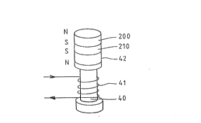
Referring now to Figure 8, an example of a non-linear
inductor of the present invention comprises a dumb-bell
shaped ferrite core or bobbin 40 carrying an inductive coil
41. A first permanent magnet 42 is bonded to one end of the
bobbin 40. Magnet 42 causes inductance L of inductor 16 -to
vary as a non-linear function of current I flowing in coil
41. A second permanent magnet 200 is located above the first
magnet 42 in such a manner that one pole of the s~cond
UK9-9]-04~ 7 ~ 3 ~
magnet 200 faces a like pole of the first mayne-t 16. The
second magnet 200 is spaced from the first magnet 42 by an
insulator 210 of invarian-t thickness. The magnet
characteristics of the first and second magnets are
substantially identical and the thickness of the insulator
is determined so that the magnetic field generated by the
non linaar inductor in use is substantially cancelled by the
second magnet. ~t will however be appreciated that, in other
embodiments of the present invention, the magnetic strength
of the second magnet may be less the magnetic strength of
the first magnet but sufficient to reduce the m~gnetic ~ield
from the non-linear inductor to an acceptable level.