Note: Descriptions are shown in the official language in which they were submitted.
- 1 - 207~
TITLE OF THE INVENTION
Information Processing Apparatus, and Elec-trode Substrate
and Information Recording Medium Used in the Apparatus
BACKGROUND OF THE INVENTION
Field of the Invention
The present invention relates to an information
processing apparatus utilizing the principle of a scanning
tunneling microscope (hereinafter abbreviated as "STM"), and
an electrode substrate and an information recording medium
used in the apparatus.
Description of the Related Art
Nowadays, memory materials are being used in computers
and apparatuses related thereto, video discs, digital audio
discs, etc., equipment constituting the nucleus of the
electronics industry. The development of new materia].s in
this field is being very actively promoted. The
characteristics required of memory material vary in
accordance with the use for which it is intended. The
following are characteristics gene.rally required of memory
material:
~ High density and large recording capacity;
~ High response speed in recording and reproduction;
- 2 - 2~7~
Low power consumption; and
Hlgh productivity and low price.
Conventionally, semiconductor memories and magnetic
memories made of semiconductors and magnetic substances have
been the mainstream of memories for information processing.
However, as a result of recent developments in laser
technology, inexpensive high-density recording mediums have
appeared which consist of optical memories using films of
organic dyes, photopolymersl or the like.
Apart from this, an STM (a scanniny tunneling
microscope) has recently been developed which makes it
possible to directly observe the electronic structure of a
surface atom of a conductor (G.Binning et al., Phys. Rev.
Let., 49,57 (1982)). With this microscope, it is possible
to perform high-resolution measurement on a real image in
space, whether it is monocrystalline or amorphous. Further,
it has an advantage that it allows the specimen to be
observed with low power without being damaged by electric
current Moreover, it can operate even in ambient
atmosphere so that it can be used with respect to various
types of materials. Thus, a wide range of applications are
expected from the STM.
The STM utilizes the fact that a tunnel current flows
when a metal probe (a probe electrode) is brought near a
conductive substance, up to a distance of approximately lnm,
- 3 -
while applying a voltage between them. This current is very
sensitive to changes in the distance between the metal probe
and the conductive substance, and even allows for the
reading of a variety of information regarding the entire
electron cloud in an actual space by performing scanning
with the probe in such a way as to maintain the tunnel
current constant. In that case, the resolution in the in-
plane dimension is approximately 0.lnm.
Thus, by utilizing the principle of the STM, there is a
good possibility that a high-density recording/reproduction
of the atom order (sub-nanometer) can be performed. For
example, in the information processing apparatus disclosed
in Japanese Patent Laid-Open Publication No. 61-80536, an
electron beam or the like is used to wri.te data onto a
recording medium by removing atom parti.cles adhering to the
medium surface, and reproducing the data by means of an STM.
According to the disclosure in the specification of U.S.
Patent No. 4,575,822, the tunnel current flowing between the
recording medium surface and the probe electrode is used to
effect recording by injecting electric charges into a
dielectric layer formed on the medium surface~ I'here has
also been a method proposed in which a laser beam, electron
beam, corpuscular beam or the like is used to perform
recording by utilizing physical or magnetic disruption of
the medium surface.
- 4 - ~ ~7~
According to another proposed rnethod, a rnaterial having
a memory effect wi-th respect to voltage/current swi-tching
characteristics, for example, a -thin-film layer of a ~-
electron-type organic compound, chalcogen compound or the
like, is used as the recording layer to perform recording
and reproduction with an STM ~Japanese Patent Laid-Open
Publication Nos. 63-161552 and 63-161553). Assuming that
the recording bit slze is 10nm, this method makes it
possible to perform recording and reproduction by as much as
1 0 10l2bit/cm2.
Fig. 8 shows a sectional view of a conventional
recording medium together with the tip of a probe electrode
202.
Numeral 101 indicates a substratei numeral 102, an
electrode layer; numeral 103, a recordi.ng layer; numeral
104, a track; numeral 202, the probe electrode; numerai 401,
a data bit recorded on the recording layer 103; and numeral
402, crystal grains generated during the formation of the
electrode layer 102. Assuming that the electrode layer 102
is formed by a usual method, such as vacuum evaporation or
sputtering, the size of the crystal grains 402 ranges from
approximately 30 to 50nm.
The distance between the probe electrode 202 and the
recording layer 103 can be kept constant -through a
conventionally well-known circuit construction. That is, a
- 5 - 2~7~9~
tunnel current flowing between the probe electrode and the
recording layer is detected, and its value is transmitted
through a logarithmic compressor 302 and a low-pass filter
303 and then compared with a reference voltage. A Z-axis
actuator 209 supporting the probe electrode is con-trolled in
such a way that this comparison value approaches zero,
thereby maintaining a constant distance between the probe
electrode and the recording layer.
Further, by driving an XY-stage 201, the surface of the
0 recording medium is traced by the probe electrode 202, and
the high frequency component of a signal at an arbitrary
point P is separated, thereby making it possible to detect
the data of the recording layer ~03. Fig. 9 shows a signal
streng-th spectrum with respect to the signal frequency at
1 5 point P at this time.
Any signals of a frequency component not higher than fo
are due to a gentle rise and fall of the substrate 101
caused by warp, distortion or the like. The signals around
f1 are due to surface irregularities of the electrode layer
103, caused mainly by the crys-tal grains 402 generated
during the formation of the material into an electrode.
Symbol f2 indicates a recording data carrier component, and
numeral 403 indicates a data signal band as shown in Fig. 6.
Symbol f3 indicates a signal component generated from the
atomic/molecular arrangement of the recording layer 103.
- 6 - ~7~
Symbol fT indicates a tracking signal, which enable~s the
probe electrode 202 to trace data arrays. Xt can be
realized by forming a groove on the medium or writing
thereto a signal which enables detection whenever an off-
track condition occurs.
Use of a conventional recording medium based on an
electrode substra-te as described above entails the following
problems:
~ To make use of the high resolution, which features
the STM, and perform high-density recording, the data
frequency component 403 must be between fl and f3. For this
purpose, a high-pass filter of a cut-off frequency of fc is
used for data component separation. However, as shown in
Fig. 9, a foot portion of the fl signal component overlaps
the data band 403. This is attributab:Le to the fact that
the f1 signal component is due to the crystal grains 402 of
the electrode layer 102, with the recording size and bit
interval of the data being in the range of 1 to lOnm, which
is close to the crystal grain size of 30 to 50nm. As a
result, the S/N ratio in data reproduction is deteriorated,
thereby increasing the incidence of error.
~ The tracking signal fT can only be placed in the
vicinity of fo. As a result, the frequency of the tracking
signal is considerably low as compared with the data
frequency, resulting in poor data tracing accuracy in
- 7 - 2~7~
tracking. This causes the incidence of error in data
reading to be lncreasedr thereby deteriorating the
reliability of the information processing apparatus.
~ Further, a track groove corresponding to such a low
tracking frequency is considerably large as compared to the
data bit size, with the result that the data recording
density is significantly low, thereby making i-t impossible
to fully make use of the high resolution featuring the STM.
1 0 SUMMARY OF T~E INVENTION
The present invention has been made in view of the
above problems in the prior art. It is an object of ~his
invention to provide an electrode substrate and a recording
medium which help to realize an unprecedentedly high density
in recording, and high S/N ratio and high-speed reading in
information reproduction, as well as an information
processing apparatus using them.
In accordance with a first aspect of the present
invention, an electrode substrate is provided comprising a
substrate and an electrode layer of a noble metal crystal
formed on the substra-te, the noble metal crystal exhibiting
a substantially linear domain boundary and a plane
orientation dispersion angle in X-ray analysis of 1~or less.
In accordance with a second aspect of the present
- 8 - ~07
invention, an information recording medium is provided
having an electrode layer according -to the above first
aspect, as a recording layer. In accordance with a third
aspect of the present invention, an information recording
medium is provided comprising a substrate, an electrode
layer of a noble metal crystal formed on the substrate, and
a recording layer provided on the electrode layer, the noble
metal crystal exhibiting a substantially linear domain
boundary and a plane orientation dispersion angle in X-ray
analysis of 1~ or less.
In accordance with another aspect of the present
invention, an information processing apparatus comprising:
an information recording medium according to the present
invention as described above; a probe electrode arranged in
close proximity to this medium; and a voltage applying
circuit for applying a pulse voltage between the medium and
the probe electrode, information being written onto the
medium by the application of the pulse voltage;
an information processing apparatus comprising: an
informat.ion recording medium according to the present
invention as described above; a probe electrode arranged in
close proximity to this medium; a first voltage applying
circuit for applying a pulse voltage between the medium and
-the probe electrode, and a second voltage applying circuit
for applying a bias voltage between the medium and the probe
- 9 - 2~
electrode, informat.ion being writ-ten on-to the medium by the
application of the pulse voltage and read from the medium by
the application of the bias voltage; and
an information processing apparatus comprising: an
information recording medium according to the present
invention as described above; a probe electrode arranged in
close proximity to this medium; and a voltage applying
circuit for applying a bias voltage be-tween the medium and
the probe electrode, information being read from the medium
by the application of the bias voltage are provided.
In accordance with a further aspect of the present
invention, an information processing method comprising the
steps of: preparing an information recording medium
according to the present invention as described above;
arranging a probe electrode in close proximity to the
medium; and applying a pulse voltage between the medium and
the probe electrode so as to write information onto the
medium;
an information processing method comprising the steps
of: preparing an information recording medium according to
the present invention as described abovei arranging a probe
electrode in close proximity to the medium; applying a pulse
voltage between the medium and the probe electrode so as to
write information onto the medium; and applying a bias
voltage between the medium and the probe electrode so as to
2~g~ ~
- 10 -
read the information from the medium; and
an information processing method compri.sing the steps
of: preparing an information recording medium according to
the present inven-tion as described above; arranging a probe
electrode in close proximity to the medium; and applying a
bias voltage between -the medium and the probe electrode so
as to read information from the medium are provided.
BRIEF DESCRIPTION OF THE DRAWINGS
1 0
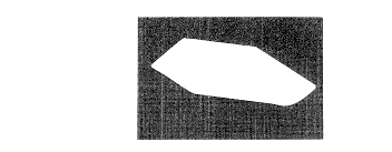
Fig. 1 shows an optical microscope image of an
electrode substrate consisting of a planar gold crystal
formed on a silicon substrate by the production me-thod of
the present invention;
Fig. 2 shows an optical microscope image of an ordinary
gold crystal;
Fig. 3 shows a small-angle X-ray diffraction spectrum
of an electrode substrate according to the present
invention;
Figs. 4(a) and ~(b) are an STM image and a surface
irregularity profile in -the Z-axis direction of the surface
of an electrode substrate according to the present
invention;
Fig. 5 i.s a sectional view of a recording medium
according to the present invention;
- 11 - 2~
Fig. 6 is a diaqram showing a frequency spectrum of a
xeproduction signal when a recording medium according to the
present invention is used;
Fig. 7 is a diagram showing -the construction of an
information processing apparatus utilizing an STMi
Fig. ~ is a sectional view of a conventional recording
medium;
Fig. ~ is a diagram showing a frequency spectrum of a
reproduction signal when a conventional recording medium is
used;
Fig. 10 is a current-voltage charac-teristic graph
according to the present invention;
Figs. ll(a) to ll(c) are sectional views of seed
substrates used in embodiments of the present invention; and
Fig. 12 is a plan view (a schematic view) of an
essential part of the surface of an electrode prepared in
accordance with an embodiment of the present invention.
DETAI~ED DESCRIPTION OF THE PREFERRED EMBODIMENTS
2~
In the present invention, the noble metal crystal of
the electrode subs-trate is preferably a planar crystal
forming a (111) plane orientation facet. Further, it is
desirable that the noble metal crystal be one grown from a
conductive substrate throuqh a hole provided in an
- 12 - 2~7~
insulating layer formed on -the conductive substrate.
Further, in the electrode substrate of the present
invention, the plane orientation dispersion angle of the
planar crystal surface ls preferably 0.6~ or less, the
aspect ratio of the noble metal crystal is 10 or more, and
the maximum surface irregularity in a lO~m square (i.e., a
square area of lO~m x lO~m) is lnm or less. Further, in the
information recording medium (hereinafter referred to simply
as "recording medium") of the present invention, it is
desirable that the maximum surface irregularity in a lO~m be
lnm or less and information be recorded by changes in the
physical conditions of the recording layer, with the
recording layer having an "electrical memory" effect.
Further, it is desirable that the recording medium have a
track, the recording layer consisting of a monomolecular
film of an organic compound or a built-up film thereof, and
the recording layer having an thickness ranging from 5 to
300A, allowing repeated recording and erasing. Further, it
is desirable that .he recording layer be formed by the
Langmuir-Blodgett's technique.
In the present invention, the term "electrical memory
effect" means the following phenomenon:
"When a thin film made of an organic compound is
arranged between a pair of electrodes and a voltage beyond a
threshold is applied to the electrodes, a transition takes
- 13 -
place from a first to a second physical condition, the first
or the second physical condition being maintained as long as
no voltage beyond the threshold is applied to the
electrodes."
Further, in the method of producing an electrode
substrate according to the present invention, it is
desirable that a structure be formed on the substrate
surface which constitutes a seed for normal metal
crystallization, as can be seen in the sectional view of
0 seed substrates in Figs. ll(a) to ll(c).
Still further, apart from using the above preferable
electrode substrate or recording medium, it is desirable, in
a preferred form of the information processing apparatus of
the present invention, tha-t the probe electrode have the
same pattern as the specifiable pattern of the electrode
substrate of the recording medium, and that the probe
electrode be of a multi-probe type.
The present invention provides a substrate electrode
having a smooth surface so as to make it possible to fully
make use of the function of an information processing
apparatus utilizLng the principle of the STM.
The present invention will now be described in detail
with reference to the drawings.
Yig. 1 shows an optical microscope image of a planar
gold crystal formed on a Si crystal substrate by the
- 19 - ~ ~7
electrode substrate producing method of the present
invention. While the gold crystal shown in Fig. 1
substantially exhibits a regular-hexagonal planar
configuration, there is also generally to be observed a
planar crystal having a threefold-symmetry axis (Fig. 2), or
an unsymme-trical deformed crystal out of the configuration
of Fig. 2. However, in the present invention, the gold
crystal clearly forms a facet surface corresponding to each
crystal surface, as shown in Fig. 1, and it has been
confirmed through an electron channeling pattern measurement
by SEM that the planar surface of the gold crystal exhibits
a (111) orientation and is substantially free from any
defects. Further, from the X-ray diffraction data shown in
Fig. 3 (measured by the X-ray diffractlon apparatus RAD3B
1 5 manufactured by Rigaku Denki), the dispersion angle of the
surface of a crystal gold electrode substrate made of a
planar crystal exhibited a (111) plane orientation
dispersion angle of 0.9~. Thus, an electrode substrate of a
very high level of orientation could be obtained. Under a
more preferable condition, an electrode substrate exhibiting
a plane orientation dispersion angle of 0.6 or less can be
obtained. Fur-ther, with a polycrystalline gold electrode
substrate, it is possible to obtain an electrode substrate
of a high level of orientation with respect to various
~5 substrate materials. The crystal domain boundary is formed
- 15 -
substantially linear (Fig. 12), and the dispersion angle in
(111) orientation is small, making it possible to obtain an
electrode substrate having a dispersion angle of 1~ or less.
Also, the ratio of the maximum diameter of the (111) surface
to the height of the planar crystal, i.e., the aspec-t ratio,
of the gold crystal is approximately 3n. Generally
speaking, a gold crystal having an aspect ratio of 10 or
more can be easily obtained, which is preferably used in -the
present inven-tion. Under a still more preferable condition,
0 a crystal having an aspect ratio of 100 or more can be
obtained.
The above planar gold substrate can be formed by the
following processes: First, I2 is dissolved in an oxidizing
solution having the property to dissolve gold, for example,
a KI aqueous solution, in order to obtain an iodine solution
ln which gold is dissolved to obtain a gold-complex aqueous
solution (in which gold is dissolved as a complex having a
structure of (AuIq)-). A substrate is immersed in this gold-
complex aqueous solution, and, to reduce the insolubility of
the gold, -the I2 is removed from the reaction system by
evaporating the same by heating or reducing the I2 to I- by
using a reducing agent, and the gold complex is
disintegrated by heating or the like to cause it to
crystall;.ze on the surface of the substrate. When the rate
of crystallization is high, a grain-cluster-like polycrystal
- 16 - 2~7~
will be generated. In view of this, the planar gold crystal
is grown by an oxidizing dissolution reaction while
balancing the etching rate with the disintegration ra-te of
the complex. This process suggests a similarity to a vapor-
phase epitaxial growth.
Fig. 4 shows an STM image of a (111) surface grown in
the manner described above. As shown in the STM image of a
l~m square (i.e., a square area of l~m x l~m) in the (111)
surface of Fig. 4(a), it may be considered that a
substantially flat smoo-th electrode substrate has been
realized in a l~m square area by using the gold crystal. As
shown in the irregularity profile in the Z-axis direction of
Fig. 4(b), its surface i.rregularities consist of atomic-
step-like long-period steps of lnm or less. With this
planar gold electrode, it is possible to provide an
electrode substrate having a still higher level of
smoothness. That is, it is possible to provide an electrode
substrate in which the difference between the highest crest
and the deepest re~ess (the maximum surface irregularity) in
a lO~m square is lnm or less and the peak value of
irregulari.ty dispersion (the dispersion peak) from the
average value of surface irregularity is 0.5nm or less.
The size of the planar gold crystal under the normal
condition ranges from l~m square to lmm square. Under
optimum conditions, it is possible to obtain a crystal
- 17 ~
having a slze of 10mm square or less, that is, several mm
square. However, it ls also possible for a crystal having a
large size of 10mm square or more to be separated, which is
controllable, though difficult. Further, it is also
possible to prepare an electrode substrate by continuously
forming minute planar crystals. Also, with such an
electrode substrate it is possible to obtain an electrode
substrate in which the (111) plane orientation dispersion
angle is smaller than that of a substrate formed by a usual
vacuum film formation method, thus making it possible to
form an electrode having an excellent orientation property.
Further, in the above production method, any material
can be used for the substrate material as long as it does
not cause a serious corrosion in the gold-complex solution.
1 5 Examples of the substrate material that can be used include:
insulating materials such as mica, ~gO, SiO2, and Si3Ns;
organic high-molecular weight materials; Si substrates
(crystalline or amorphous), which are conductive materials;
graphite (HOPG); and various metal substrates and substrates
of compounds thereof.
However, a difference was observed in the ease with
which the gold crystal was separated depending upon the type
of substrate used. By utilizing such a difference in gold-
crystal separation characteristics between different types
of substrates, it is possible to selectively generate and
- 18 - 2~7~9~
grow the planar gold substrate at desired positions.
Further, although the character.is-tics of the planar
crystal and the production method -thereof have been
described with reference to the case where gold is adopted
as the material, the planar crystal to be grown is not
restricted to a gold crystal. A similar technique is also
applicable to noble metal materials allowing the formation
of a complex halide, such as Pt, Pd, Rh, and Ir. Further,
it is also applicable to a complex cyanide and a complex
sulfite.
Fig. S is a sectional view of a recording medium using
an electrode substrate according to the present invention.
Numeral 101 indicates a substrate; numeral 102, an electrode
layer having a smooth surface; numeral 103, a recording
1 5 layer; numeral 104, a track; numeral 202, a probe electrode;
and numeral 401, a data bit.
The recording layer may be formed of a material capable
of developing a memory-switching phenomenon (an electrical
memory effect) having current-voltage characteristics, as
for example, an organic monomolecular film or a built-up
film thereof, having molecules each including both a group
having a ~.electron level and a group having a 6 electron
level deposited only on the electrode. Due to the
electrical memory effect, it is possible to reversibly
effect transition (switching) between a low-resistance
condition (ON condition) and a high-resistance condition
19- 2~7~
(OFF condition) (the ON and OFF conditions in Fig. 10) by
applying a voltage beyond a threshold which enables
transition, with an organic molecular film as described
above, a built-up film thereof, or the like, being arranged
between a pair of electrodes. Further, each of the
conditions can be maintained ~stored in memory) wi-thout
applying any voltage.
Generally speaking, most organic materials exhibit an
insulating or semi-insulating property. Thus, the organic
materials that can be applied to the presen-t invention,
which contain a group having a ~ electron level, include an
extremely wide range. Examples of a dye having a ~ electron
system which is suitable for the present invention, include:
dyes having a porphyrin skeleton, such as phthalocyanine and
tetraphenylporphyrin; azulene-type dyes having a squalilium
group and a croconic methine group as a bonding chain; dyes
similar to a cyanine type or cyanine dyes in which two
nitrogen-containing complex rings, such as quinoline,
benzothiazole, or benzooxazole, are connected by a
squalilium group and a croconic methine group; condensed
polycyclic aromatic compounds, such as anthracene and
pyrene; chain compounds formed by polymerization of an
aromatic cyclic compound or a complex cyclic compound; a
polymer of a diacetylene group; a derivative of
-tetracyanoquinodimethane or tetrathiafulvalene and an analog
- 20 - ~ ~r~
thereof or a charge-transfer complex thereof; and a metal
complex compound such as ferrocene and trisbipyridine
ruthenium. Further, examples of a polymer material suitable
for the present inven-tion include a condensation polymer of
polyimide, polyamide or the like, and biopolymers such as
protein.
The electrical memory effect of these compounds having
a ~ electron level has been observed on examples having a
film thickness of several tens of nm or less. From the
viewpoint of film formation characteristic and uniformity, a
preferable film thickness is in the range of 5 to 300A.
In another form of the present invention, the recording
layer 103 is not absolutely necessary. As stated in Phys.
Rev ~ett., 65, 2418 (1990) by H.J. Mamin et al., it is
possible to directly cause a perturbation on the surface of
the electrode layer 102 so as to selectively generate a
disturbance thereon, for example, by depositing fine gold
particles on the electrode surface through field evaporation
of gold by using a gold probe electrode. According to the
above reference, this field evaporation of gold varies
somewha-t depending upon the distance between the electrode
surface and the tip of the probe elec-trode. With an
application voltage of 3.2V or less, the probability that
the field evaporation of gold will take place is zero.
2~ However, when a voltage of 3.5V to 4V is applied, the
- 21 - 2Q7~
probability -that the field evaporatlon of gold occurs is
100~. The pulse width which allows recording at this time
is l~m or less, making it possible to cope with high-speed
recording. The pit diameter varies depending upon various
conditions. ~sually, recording with a pit diameter of 100
to 300A is possible, and under more preferable conditions,
recording can be effected with a pit diameter of 30 to lOOA,
and further, 30 to 70A. In the vacuum evaporation of a
noble metal, a grain cluster of 300 to 500A is usually
generated, so that it is rather difficult to clearly
distinguish the recording from the surface irregularities on
the electrode substrate. Therefore, in the present
invention, use of a smooth electrode substrate according to
the present invention is indispensable. The direction of
the field evaporation largely depends upon the surface
condition of the smooth substrate electrode, and the above-
described phenomenon occurs regardless of the polarity of
the application electrode. That is, by making the polarity
on the side of the probe electrode positive, deposition of
~ine gold particles takes place on the substrate electrode
surface, as described above. If, conversely, a positive
application is effected on the substrate electrode side, the
deposltion of gold on the substrate electrode surface takes
place in the same way, although the threshold voltage
thereof increases. However, it is also possible to position
- 22 -
the probe electrode on a minute gold protrusion on the
substrate electrode surface and remove the gold pro-trusion
by applying a voltage (erasable).
Although methods of directly imparting a perturbation
to the electrode layer have been described, it is also
possible, as shown in Fig. 5, to provide the recordi.ng layer
103 on a smooth electrode surface and selectively cause
changes in the conditions of the recording layer, including
changes in the configuration thereof, thereby effecting
recording. Regardi.ng the material to be employed for the
recording layer, it is possible to use an organic com~ound
which allows changes in configuration to take place through
irradiation of various types of energy at low levels as
described below. Further, by effecting recording through
changes in the conditi.on of individual organic molecules, it
is possible to obtain a recording density on a molecular
scale.
1) A method of effecting local changes in the structure
and orientation of a molecular aggregate formed on the
recording layer.
For example, a change i.s caused in the physical
structure of an LB film by using a local current and an ion
current generated through a probe current or an electric
field effect, thereby causing a local variation in the film
thickness of the ~B film so as to effect recording. As
- 23 ~ 7~
described below, to ob-tain an organic thin film having a
high level of orientation, a method using an LB film is -the
optimum one known at present.
Further, as a recording method of this type, a method
is available according to which changes in the orientation
of a liquld crystal ma-terial under an electric field are
utilized.
2) A method of causing local changes in the molecular
or electronic structure of the recording layer using the
above local current and ion curren-t generated through a
probe current or an electric field effect.
Further, it is possible to cause changes in the film
struc-ture as a result of a local oxidation-reduction
reaction, thereby effecting recording.
3) A method of causing changes in an electron condition
accompanying a local polymerization by using the above local
current and ion current generated through a probe current or
an electric field effect.
A monomer used in the method may be:
Rl- (CH2) -n-X-R2 (where 10 < n _ 25,
X = -COO-, -CONH-, -OCO-
Rl = -CH3, -CH = CH2
R2 = -H, -CH = CH2, -C (CH3) = CH2, -CH2CH = C}12
(R2 iS not -H when Rl iS -CH3) )
~) A method of directly effecting recording by virtue
- 2~ - 2~74~1~
of changes in molecular conformation or molecular
configuration using the ahove local current and ion current
generated through a probe current or an electric field
effect.
For example, the following compounds can be used in
this method:
(A) a compound which is a derivative of spiropyran,
fulgide, or azobenzene and which has a photochromic
characteristic; and
(B) a compound in which changes occur because of dye
association, as for example, a melocyanine compound.
In the above-described methods, recording may be
effected separately. Generally, however, it is often
realized in the form of a combination of a number of
effects.
Specifically, the formation of the recording layer 103
may be effected by evaporation, the cluster ion beam method
or the like. However, from the viewpoint of
controllability, facility and reproduclbility, the LB method
is the most suitable of the conventional methods known in
the art. With the LB method, a monomolecular film of an
organic compound having in one molecule a hydrophobic
portion and a hydrophilic portion, or a built-up film
thereof, can be easily formed on a substrate, thereby making
it possi.ble to stably provide an organic ultra-thin film
- 25 - ~ ~7~
which has a thickness of a molecular order and which is
uniform and homogeneous over a wide area. Accordingly, it
is possible to prepare a recording medium which reflects the
surface property oE an under-coat electrode substrate as it
lS.
In accordance with the LB method, a monomolecular film
or a built-~p film thereof is formed by utilizing the fact
that in molecules each having a structure in which
hydrophilic and hydrophobic por-tions exist therein, an
appropriate balance is maintained between them, the
molecules form a monomolecular layer on a water surface,
with the hydrophilic groups facing downwards. Examples of
the group constituting the hydrophobic portion include
various types of hydrophobic groups, such as generally well-
known saturated and unsaturated hydrocarbon groups,condensed polynuclear aromatic groups, and chain polycyclic
phenyl groups. One, or a plurality of types of such groups,
are combined to form the hydrophobic portion. Most typical
examples of the group forming the hydrophilic portion
include various types of hydxophilic groups, such as
carboxyl group, ester group, acid amide group, imide group,
hydroxyl group, and amino group (of first, second, third or
fourth grade). One, or a plurality of types of such groups,
are combined to form -the above-mentioned hydrophilic
portion.
- 26 - 2~7~
With an organic molecule including such hydrophobic and
hydrophilic groups in a well-balanced manner and having an
appropriate size, it is possible to form a rnonornolecular
film on the surface of water, thus providing a material
which is very suitable for the present invention.
In the present in-vention, the tip of the probe
electrode 202 must be as pointed as possible so that the
resolution in recording and reproduction may be improved.
It is generally known that a probe electrode having an
atomic resolution can be prepared by an electrolytic
polishing method, such as the tungsten method. However, in
view of the problem of a surface oxide film or the like, it
is possible to employ a probe electrode prepared by
mechanically polishing the tip of a 10 thick platinum bar
into a cone of 90~ and evaporating the surface atoms through
application of an electric field in an ultra-high vacuum.
It is known that a probe electrode prepared in this way has
an atomic resolution. However, the configuration and
processing method of -the probe electrode are not restricted
to those described above.
Fig. 6 shows the signal frequency spectrum of a signal
at point P in the information processing apparatus of the
present invention shown in Fig. 7.
Fig. 7 shows an example of the construction of an
information processing apparatus utilizing the principle of
- 27 - 2~7~
the STM, which will be described below with reference to the
drawing. Numeral 101 indicates a substrate; numeral 102, a
metal electrode layer; and numeral 103, a recording layer.
Numeral 201 indicates an XY stage; numeral 202, a probe
electrode; numeral 203, a support member for the probe
electrode; numeral 209, a linear actuator for driving the
probe electrode 204 in the Z-directioni numerals 205 and
206, linear actuators for driving the XY stage in the X- and
Y-directions, respectively; and numeral 207, a pulse voltage
circuit.
Numeral 301 indicates an amplifier for de-tecting a
tunnel current flowing from the probe electrode to the
electrode layer 102 by way of the recording layer 103.
Numeral 302 indicates a logarithmic compressor for
1 5 converting a change in the tunnel current into a value which
is proportional to the gap distance of the recording layer;
and numeral 303 indicates a low-pass filter for extracting
surface irregularity components of the recording layer.
Numeral 304 indica-tes an error amplifier for detecting an
error between a reference voltage VREF and the low-pass
filter 303; and numeral 305 indicates a driver for driving
the actuator 204. Numeral 306 indicates a drive circuit for
performing position control of the XY stage. Numeral 307
indicates a high-pass filter for separating data components.
Any signals of a frequency component not higher than fo
- 2~ 9 ~ ~
are due to a gentle rise and fall of the substrate 101 due
to warp, distortion or the like. Symbol f2 indicates a
recording data carrier component, and numeral 403 indica-tes
a data signal band. Symbol f3 indica-tes a signal component
generated from the atomic/molecular arrangement of the
recording layer, and symbol fT indicates a tracking signal.
A signal around f1 is due to a slight irregularity of the
surface of the electrode layer 102, i.e., the (111) surface.
This irregularity is made equal to or smaller than the
recording signal. In recording and reproduction utilizing
the STM, the change in this irregularity approximately
corresponds to five layers of electrode materials (lnm or
less). Further, with a recording medium according to the
present invention, the size of the smooth surface of the
surface of the recording layer 103 is l~m square. Under a
more favorable condition, lO~m or more. This provides the
following advantages:
~ The signal component f1 due to the surface
irregularities of the recording layer 103 and the data
signal component 403 do not overlap each other, and there is
no deterioration in S/N ratio due to the expansion of the f
spectrum. That is, it is possible to reduce the incidence
of error in data reading.
~ It is possible to place -the tracking signal fT in the
vicinity of the data signal component 403. That is, the
2 ~
- 29 -
tracking frequency can be made high, thereby making it
possible to ensure a satisfactory accuracy in tracking.
~ Further, because of the high tracking frequency, a
configurati.on approximately the same as the data bit size
suffices when forming a groove for -tracking on the recording
medium, thus making it possible to effect tracking without
sacrificing the recording densi-ty.
~ Also, since there is no irregularity on the surface
of the recording layer 103, the amount of displacement in
the Z axis direction is srnall when performing XY scanning
while keeping the distance between the surface of the
recording layer 103 and the probe electrode 202 constant.
This makes it possible to drive the XY stage 201 at a very
high speed. As a result, it is possible to perform high-
1~ speed reading and writing of data.
~ Since there is no irregularity on the electrodesubstrate, the position of the tip of the probe electrode,
that is, the position of the tip atom through which the
tunnel current flows, can be selected to attain stability.
A phenomenon in which a tunnel current flows between a
plurality of atoms of the probe electrode and the recording
layer as in the case of an electrode substrate having an
irregularity, i.e., the so-called ghost phenomenon, does no-t
occur, thus enabling a highly reliable reading.
Examples
- 30 - 2~9~
Example 1
An iodine solution was prepared by dissolving 4g of
potassium iodide (KI) and 0.6g of iodine ~I2) in 50ml of
pure water. Then, a 5000~ thick gold film formed by vacuum
evaporation (approximately 0.08g in terms of weight) was
completely dissolved in the iodine solution to obtain a
gold/iodine-complex stock solution. lOml of this stock
solution was pipetted and diluted in 50ml of pure water to
prepare a reaction mother liquor. A silicon substrate whose
natural oxide film had been etched by hydrofluoric acid was
immersed in the mother liquor and heated to 80~C on a hot
plate. When, as a result of sublimation of the iodine, the
solution had become a transparent thin-yellow color, a flat
gold crystal was separated. Upon observation with an
1 5 optical microscope, a flat crystal was observed all over the
substrate. Upon measurement, the plane orientation
dispersion angle of this electrode substrate was found to be
0.9~. Next, upon observation of the surface of the flat
gold crystal with an STM, it was found that the maximum
surface irregularity and dispersion peak in a lO~m square of
this substrate were 0.8nm and 0.4nm, respectively.
Subsequently, a track 104 having a width of O.l~m, a
pitch of l.O~m, and a depth of 50A was formed on the surface
of the flat gold crystal electrode by a focused ion beam.
The focused ion beam process was conducted by using gold
- 31 - ~7~
ions under the following conditions: acceleration voltage:
40KV; ion current: 14pA; dose amount: 1.0 x l.016/cm2.
A four-layered polyimide LB film was :Eormed on the
smooth electrode substrate, prepared in the above-described
manner, as the recording layer 103. The recording layer 103
was formed by uslng the polyimide LB film as follows.
A polyamide acid as shown in formula (1) was dissolved
in an N,N'-dimethylacetamide/benzene mixture solution of 1:1
(V/V) (density in terms of monomer: 1 x 10⁻³M). Then, it
was mixed with a separately prepared 1 x 10⁻³M solution of
N,N'-dimethyloctadecylamine in the same solvent in a
proportion of 1:2 (V/V) to prepare a polyamide-acid-
octadecylamine salt solution as shown in formula ~2).
H O ~ - N ~ ~
N - C - OH Formula (1)
_ H O O _n
H3C (CH2) ,s ~ H (CH3) 2
O O H
O --C ~ ~ ~ > - Formula (2)
----N - C --O HN~ (CH3)2
l 11 11 1
H O O (CH2) ,sCH3 n
25 This solution was developed on a water phase consisting
- 32 -
of pure water at a temperature of 20~C to form a
monomolecular film on the surface of the water. After
removing the solven-t by evaporation, -the surface pressure
was augmented to 25 mN/m. While keeping the surface
pressure constant, the above substrate electrode was gently
immersed in such a way as to traverse the water surface at a
rate of 5 mm/min, and was then pulled up gently at a rate of
5 mm/min to prepare a two-layered Y-type monomolecular
built-up film. By repeating this operation, a four-layered
monomolecular built-up film of polyamide-acid-oc-tadecylamine
salt was formed. Subsequentl.y, this substrate was
calcinated by heating for thirty minutes at 200~C under a
reduced pressure (~ 1 mmHg) to imidize the polyamide-acid-
octadecylamine salt (Formula 3), thereby obtaining a four-
layered polyimide monomolecular built-up film.
H3C (CH2),s - N~ H (C~l3)2
- O O ~1 -
o-c~c~
-- N--C C O HNr (CH3)2
20 H O O (CH2)~sCH3 _ n Formula (3)
O O
- \C~ ~C/
_ O O _ n
Subsequently, the surface configuration of a recording
- 33 - ~ ~7~
medium prepared in the above-described manner was examined
on the information processing apparatus shown in Fig. 7.
Upon examination, it was found that the surface of the
recording medium reflected the smoothness of the electrode
and the track 104. In a lO~m square, the track 109 had been
formed to a depth of 50A, and, outside the track 104, the
maximum surface irregularity was 0.9nm, with the dispersion
peak being 0.4nm. Accordingly, the track 104 could be
clearly distinguished.
1~ Next, a recording/reproduction experiment was
conducted. A platinum/rhodium probe electrode 202 was used
as the probe electrode 202. The probe electrode 202 is used
for the purpose of controlling the distance (Z) between it
and the recording layer 103, and is under a fine current
control to a constant level. Further, the linear actuators
204, 205 and 206 are designed such that they allow fine
control also in the in-plane (X, Y) directions while keeping
the distance Z constant.
Further, the probe electrode 202 is capable of directly
effecting recording, reproduction and erasing.
Addit.ionally, the recording medium is placed on the high-
precision XY stage 201 and can be moved to an arbitrary
position.
The recording layer 103, comprisi.ng a four-layered
polyimide film as described above, was placed on the XY
_ 39 _ 2~7~9~
stage 201. Then, a voltage of +1.5V was applied between the
probe electrode 202 and the electrode layer 102 of the
recording medium, and the distance (Z) between the probe
electrode 202 and the surface of the recording layer 103 was
adjusted while monitoring the current. A-t this time, a
probe current Ip for controlling the dis-tance Z between the
probe electrode 202 and the surface of the recording medium
was set in such a way that 10-1~A _ Ip < 10-11A.
Subsequently, information recording was conducted at a
pitch of 100A while performing scanning with the probe
electrode 202. In conducting the information recording, the
probe electrode 202 was positioned on the + side and the
electrode layer 102 on the - side, applying a rectangular
pulse voltage beyond a threshold voltage VthON causing the
electric memory material (the four-layered polyimide film)
to be changed to a low-resistance cond:Ltion (ON condition).
Afterwards, the probe electrode 202 was brought back to the
recording start point, and was caused to scan the recording
layer 103 again. Here, adjustment was made in such a way
that Z was constant at the time of reading of the recorded
information. As a result, it was shown that in the
re~ording bit, a probe current of approximately 10nA flowed,
under the ON condition.
Further, the probe voltage was set at 10V which is
above the threshold voltage VthOFF causing the electric
9 ~ ~
- 35 -
memory material to change from the ON to the OFF condition.
The recording position was traced again to confirm that this
caused -the entire recording conditions to be erased, thereby
causing the material to be changed to the OFF condition.
Still further, a recording pulse was applied in
accordance with the above recording method to a position
which was in the OFF condition with the recording condition
erased to confir~ that it caused the material to be changed
to the OFF condition. It was also confirmed that the
recording condition could be erased again.
Example 2
Using the mother liquor described in Example l,
eleetrode layers were formed on different types of
substrates, and an experiment similar to tha-t of Example l
was condueted thereon. Table l shows the surface properties
of the electrode layers used in the experiment.
Table l
Substrate Dispersion Surface irre~ularity (in 10~m square)
type angle Maximum surface Dispersion peak
20 . irregularit~
Si (etched) 0.9~ 0.8nm 0.4nm
HOPG 0.6~ 0.7nm 0'.3nm
Au/Si 0.9~ 0.8nm 0.4nm
Cr/Si 0.9~ 0.8nm 0.4nm
25Al/Si 0.9~ 0.9nm 0.4nm
a-Si/SiO2 (thermal 0.9~ 0. 9nm 0.4nm
- 36 - 20~ ~9~ ~
oxidation film)
Glass 1.0~ l.Onm 0.9nm
SiO2/Si (thermal 0.9~ 0.3nm 0. 4nm
oxidation film)
SiN/Si l.. 0~ 0.9nm 0.4nm
MgO 0. 6~ 1. Onm 0.4nm
Polyimide (ca}~ton) 1.0~ 1. lnm O.4nm
Recording mediums prepared by using the electrode
substra-tes of Table 1 were examined for surface
0 configuration on the information processing apparatus shown
in Fig. 7. The surface of each recording mediwn reflected
the smoothness of the electrode and the track 104. In a
lO~m square, the track 104 had been formed 50A deep, and the
maximum surface irregularity outside the track 104 was 0.9nm
or less, with the dispersion peak being 0.4nm or less.
Therefore, as in Example 1, the track 104 could be clearly
distinguished. Next, an experiment was conducted on
recording, reproduction and erasing, and it was confirmed
through the experiment that recording, reproduction and
erasing could be performed as in Example 1.
Example 3
A planar gold crystal like that of Example 1 was formed
under the same experimental conditions as in Example 1
except that instead of taking the iodine out of the reaction
system by sublimation, the iodine was reduced by using
reducing agents. The smoothness of this crystal, too, was
2~743~
substantially the same as that of Example 1. The reducing
agents used in the experiment were sulfite ions and
hydroquinone. The substrate was a silicon substrate and the
crystallization temperature was 60~C.
Example 4
An experiment was conducted in which the gold
concentration of the stock solution of Example 1 and the
crystallization temperature were varied. The results are
summarized in Table 2. The substrate used was a silicon
crystal substrate.
Table 2
Amount of Crystalli- Average Dispersion Average ~;r~1m
gold zation facet angle surface
dissolved temperature diameter irregularity
. (g) ('C) (lO~lm square)
0.08 70 300~m 0.6~ 0.9nm or less
0.08 75 200~m 0.6~ 0.9nm or less
0.1 65 350~m 0.6~ 0.9nm or less
0.1 70 300~m 0.6~ 0.9nm or less
0.1 80 150~m 0.8~ 0.9nm or less
0.12 65 500~m 0.5~ 0.9nm or less
0.12 70 350~m 0.6~ 0.9nm or less
0.12 75 200~m 0.6~ 0.9nm or less
0.17 65 600~m 0.4~ 0.9nm or less
0.17 70 ~50~m 0.5~ 0.9nm or less
Ø17 75 200~m 0.7~ 0.9nm or less.
- 38 - 2~7~
Example 5
A silicon substrate and a glass (SiO2) substrate which
had been surface-processed by various well-known methods in
such a manner that the matrix intersections at intervals of
500~m were made l~m to 2~m square were immersed in the
mother liquor used in Example 1 to observe how
crystallization took place under the same conditions as in
Example 1.
Each of the seed substrates for selective deposition
0 used in the experiment was prepared in the following manner:
~ A silicon substrate having a thermal oxidation film
(having a thickness of 500 to lOOOA) was prepared and the
thermal oxidation film was etched by HF by using AZ1370
(manufactured by Hoechst) as a photoresist to form a seed
1 5 pattern.
~ A 1OOOA thick silicon nitride film was formed by the
low-pressure CVD method on the silicon substrate from which
the surface na-tural-oxidation film had been removed by
etchi.ng. Then, a CF4 reactive ion etching was performed
thereon by using AZ1370 as a photoresist to form a seed
pattern.
~ A lOOA thick photosensitive polyimide LB film was
formed on the silicon substrate from which the natural-
oxidation film had been removed by etching, and an etching
pattern was formed thereon as a seed pattern.
- 39 -
~ A resist pa-ttern of AZl370 was formed on the silicon
substrate from which -the surface natural~oxidation film had
been removed by etching. Then, gold was deposited to a
depth of lOOA by resistance heating vacuum evaporation, wi.th
a 30A thick chromium film being used as an under-coat layer,
to form a seed pattern through li.ft-off.
~ Using a silicon substrate having a lOOOA thick
thermal oxidation film, a seed pattern was formed in the
same way as in ~.
~ An amorphous silicon film was formed to a thickness
of lOOOA by the GD method on a well-cleaned coning #705g
glass substrate. Etching was performed thereon by CF~
reactive ion etching by using AZl370 as a photoresis-t to
form a seed pattern.
~ A seed pattern was formed on the si~icon substrate
by ion implantation of Au++ ions accelerated at 40kV, using
JIBL-lOOA (manufactured by Nippon Denshi) as the FIB
apparatus, under the following conditions:
ion current value: 30pA; and
ion implantation amount.: l x lO1s ions/cm2.
The results o~ the experiment on the seed substrates
are summarized in Table 3.
- 40 - ~ ~7~91~
Table 3
Surface configuration & material Grystallization
Fig. ll~a) SiO2/Si Selective deposition observed
SiN/Si Selective deposition observed
Slight crystal growth
observed on a part of SiN
surface
Polyimide/Si Selective deposition observed
Eig. ll(b) Au(/Cr)/Si Selective deposition observed
~0 Very slight crystal growth
also observed on Si surface
Au(/Cr)/S io2 Selective deposition observed
. a-Si/SiO2 Selective deposition observed
Fig. ll(c) Si. substrate Selective deposition observed
Au-ion-beam- Very slight crystal growth
processed also observed on Si surface .
Next, as in Example 1, four layers of polyimide
monomolecular films were accumulated on an electrode
substrate prepared by the method ~ to form a recording
medium, which was examined for surface configuration on the
information processing apparatus shown in Fig. 7. The
surface of the recording medium reflected the smoothness of
the electrode, and the maximum surface irregularity in a
10~m square was 0.9nm or less, with the dispersion peak
being 0.4nm or less.
- 41 -
The planar gold crystal selectively deposited formed a
(111) plane orientation facet, which was in the same pattern
as the seed pattern used. Further, the edges of the facet
reflected the characteristics of the crystal surface so as
to provide a -track of a very hiqh degree of linearity (see
Fig. 12). The track groove formed was deep, so that the
track could be clearly distinguished as in Example 1.
Next, an experiment was performed on recording,
reproduction and erasing, and it was confirmed that
recording, reproduction and erasing could be performed as in
Example 1 with an electrode substrate prepared in the above-
described manner. Further, it was also confirmed tha-t
recording, reproduction and erasing could be performed with
electrode substrates prepared by other methods as described
above.
Example 6
1 normal sodium hydroxide was added to a commercial
gold sulfite plating liquid (Newtronex 309 manufactured by
Nippon Retroplating Engineers Kabushiki Kaisha) to adjust
the solution to a pH of 13. Then, a silicon crystal
substrate, a glass substrate, and gold and aluminum
deposition substra-tes were separately immersed therein and
observed for crystallization. Growth of a planar gold
crystal was observed on the silicon crystal substrate and
the aluminum deposition substrate.
2 ~
- 42 -
It is to be assumed that regarding the s~bstrate
selectivity in this case, the formation of a local cell as a
result of the dissolution of the substrate is predominant,
and a material having a higher degree of ionization tendency
than that of gold allows selective deposition. Therefore, a
selective deposition of gold as shown in Example 6 is also
possible with a combination of the selective deposition
according to the method of Example 5 and the crys-tal growth
process shown in Example l.
Example 7
l.4g of potassium iodide and 0.6g of iodine I2 were
dissolved in 50ml of pure water to prepare an iodine
solution. Then, a 5000A thick gold film (about 0.08g in
terms of weight) formed by vacuum evaporation was completely
dissolved in the iodine solution to prepare a gold/iodine-
complex solution as a stock solution, lOml of which was
pipetted and diluted in 50ml of pure water to prepare a
reaction mother liquor~ A silicon substrate whose natural
oxidation film had been etched with hydrofluoric acid was
immersed in the mother liquor and was hea-ted on a hot plate
at 80 C. When the iodine had been sublimed and the solution
became a transparent thin yellow, a planar gold crystal was
separated. Upon examination with an optical microscope, a
planar crystal was observed all over the substrate surface.
Upon measurement, the plane ori.entation dispersion angle of
- 93 -
this electrode substrate was 0.9~. Next, upon observation
with an STM of the surface of the planar crystal, it was
found tha-t the maximum surface irregularity in a lO~m square
was 0.8nm and the dispersion peak was 0.4nm.
Subsequently, a track 104 having a width oE O.l~m, a
pitch of l.O~m and a dep-th of 5.0A was formed on the surface
of the planar gold crystal electrode by a focused ion beam,
using gold ions under the following conditions:
acceleration voltage: 40KV; ion current: 14p~; nd dose
10 amount: 1.0 x 10l6/cm2.
Then, using the gold electrode substrate which had been
prepared by the above-described method, an examina-tion was
made to evaluate surface configuration on the information
processing apparatus shown in Fig. 7. The surface of the
recording medium reflected the smoothness of the electrode
and the track 104, which had been formed to a depth of 50A
in a lO~m square, exhibiting a maximum surface irregularity
of 0.9nm and a dispersion peak of 0.4nm. Accordingly, the
track 104 could be clearly distinguished. Next, a gold wire
having a diameter of 250~m was formed into a gold chip
through electrolytic polishing in concentrated hydrochloric
acid (1.5 to 2 Vdc), thereby preparing a gold probe
electrode 202, which was used in an experiment on recording
and reproduction. The probe electrode 202 is intended for
the control of the distance (Z) between it and the recording
- ~4 - ~ 91~
layer 103, and is under a fine current control to at-tain a
constant level. Further, the linear actuators 204, 205 and
206 are so designed as to allow fine motion control in the
in-plane directions (X, Y) while rnaintaining the distance Z
constant.
Further, the probe electrode 202 is capable of directly
performing recording, reproduction and erasing. Moreover,
the recording medium is placed on the high-precision XY
stage 201 and can be moved to an arbitrary position.
The above-mentioned gold substrate electrode was placed
on the XY stage 201. Then, a voltage of +1.5V was applied
between the probe electrode 202 and the gold substrate
electrode 102, and the distance (Z) between the probe
electrode 202 and the recording medium 103 was adjusted
while monitoring the current. Here, a setting was made in
such a manner that the probe current Ip for controlling the
distance Z between the probe electrode 202 and the surface
of the recording medium 103 was kept in the range: 10-1~A _
Ip _ 1O~1lA.
Next, information recording was conducted at a pitch of
loOA while performing scanning with the probe electrode 202.
The information recording was effected by applying a
rectangular pulse voltage equal to or higher than the
threshold voltage Vt~lON of field evaporation of gold
(Usually, vol-tage: 4V; and width: 350ns), with the probe
- ~5 - 2~7~
electrode 202 placed on the -~ side and the gold substrate
electrode 102 on the - side. Afterwards, the probe
electrode 202 was brought back to the recording start polnt,
and was made to scan the recording layer 103 again. Here,
adjustment was made so that Z is constant at the -time of
information reading. As a result, it was shown that in a
recording bit, a probe current of approximately 10 nA flows,
with fine particles of gold being accumulated.
Example 8
A gold substrate electrode was formed in the same
manner as in Example 7. A two-layered spiropyran LB film
was formed on the prepared gold substrate electrode, thereby
preparing the recording layer 103. In the following, a
description will be given on how the recording layer 103
using the spiropyran LB film was formed.
A mixture solution of a spiropyran derivative with an
octadecyl group introduced therein and arachidic acid in the
proportion of 1 : 2 (solvent: chloroform in a concentration
of 1 x 10⁻³M) was developed on a water phase consisting of an
aqueous solution of CdCl2 (concentration: 1 x 10⁻⁹M) at a
temperature of 20~C to form a monomolecular film on the
water surface. After removing the solvent by evaporation,
the surface pressure was raised up to 30 mN/m. While
keeping the surface pressure constant, the above substrate
electrode was gently immersed in such a way as to traverse
- ~6 - 2~7~
the water surface at a rate of 5 mm/rnin. Then, it was
gently pulled up, thereby forming a two layered Y-type
monomolecular built-up film.
Next, using the recordlng medlum prepared by the method
descrlbed above, an examlna-tlon for surface conflguration
was conducted on -the lnformatlon processlng apparatus shown
ln Flg. 7. It was found -that the surface of the recordlng
medlum reflected the smoothness of the electrode and the
track 104, whlch had been formed to a depth of 50A ln a lO~m
square, and the maximum surface irregularlty outslde the
track 104 was 0.9nm or less, wlth the dispersion peak belng
0.4nm or less. Accordlngly, the track 104 could be clearly
dlstlngulshed as in Example 7. Next, an experlment on
recording and reproductlon was conduc-ted, and lt was
confirmed that recordlng and reproductlon could be performed
as ln Example 7. As to the recordlng blt dlameter,
measurements ranglng from approxlmately lOA to 50A could be
ascertalned (recordlng voltage: 3.2V; wldth: 350 nsec). It
was found that the average bit diameter taking into account
the incidence of occurrence was approximately 16A~.
Example 9
Uslng the mother llquor descrlbed ln Example 7,
electrode layers were formed on varlous types of substrates,
and an experlment slmllar to that of Example 7 was
conducted. The surface propertles of the electrode layers
_ 47 - 2~7~91~
used i.n the experiment are summarized in Table 1 (shown
above).
As shown in Table 1, the surface of each recording
medium reflected the smoothness of the electrode and the
track 104. In a lO~m square, the -track 104 had been formed
50A deep, and the maximum surface irregularity outside the
track 104 was 0.9nm or less, with the dispersion peak being
0 4nm or less. Therefore, as in Example 7, the track 104
could be clearly distinguished. Next, an experiment was
conducted on recording, reproduction and erasing. It was
confirmed that recording, reproduction and erasing could be
performed as in Example 7.
Further, a recording/reproduction experiment similar to
that of Example 7 was performed using a spiropyran LB film
as the recording layer, as in Example 8, and it was
confirmed that recording and reproduction could be performed
as in Example 7. Also, the average bit diameter was
substantially the same value.
Example 10
~0 A sil.icon substrate and a glass (SiO2) substrate which
had been surface~processed by various well-known methods in
such a way as to make the matrix intersections at intervals
of 500~m l~m to 2~m square were immersed in the mother
liquor used in Example 7 to observe how crystallization
occurred under the same conditions as in Example 7.
- 48 -
~7~
Each of the seed substrates for selective deposition
used in the experiment was prepared in the following manner:
~ A silicon substrate having a thermal oxidation film
(having a thickness of 500 to loOOA) was prepared and the
thermal oxidation film was etched by HF by using AZ1370
(manufactured by Hoechst) as a photoresis-t to form a seed
pattern.
~ A lOOOA thick silicon nitride film was formed by the
low-pressure CVD rnethod on the silicon substrate from which
the surface natural-oxidation film had been removed by
etching. Then, a CF4 reactive ion etching was performed
-thereon by using AZ1370 as a photoresist to forrn a seed
pattern.
~ A lOOA thick photosensitive polyimide LB film was
1 5 formed on the silicon substrate from which the natural-
oxidation film had been removed by etching, and an etching
pattern was formed thereon as a seed pattern.
~ A resist pattern of AZ1370 was formed on the silicon
substrate from which the surface natural-oxidation film had
been removed by etching. Then, gold was deposited to a
depth of lOOA by resistance heating vacuum evaporation, with
chromium being used in the form of a 30A thick under-coat
layer, -to form a seed pattern through lift-off.
~ ~sing a si.licon substrate having a lOOOA thick
thermal oxidation film, a seed pattern was formed i.n the
- 49 -
same way as in ~.
~ An amorphous silicon film was formed to a thickness
of lOOOA by the GD method on a well-cleaned coning ~7059
glass substrate. Etching was performed thereon by CF4
reactive ion etching using AZl370 as a photoresist so as to
form a seed pattern.
~ A seed pattern was formed on the silicon substrate
by ion implantation of Au~ ions accelerated at 40kV, using
JIBL-lOOA (manufactured by Nippon Denshi) as the FIB
apparatus, under the following conditions:
ion curren-t value: 30pA; and
ion implantation amount: l x 1015 ions/cm2.
The results of the experiment on the seed substrates
are summari~ed in Table 3 (shown above).
Next, an electrode subs-trate prepared by the method
was examined for surface configuration on the information
processing apparatus shown in Fig. 7. The maximum surface
irregularity in a lO~m square was 0.9nm or less, with the
dispersion peak being 0.4nm or less.
It was found that the edges of the facet of the planar
gold crys-tal selectively deposited reflected the
characteristics of the crystal surface so as to provide a
track of a very high degree of linearity. The track groove
formed was deep, so that the track could be clearly
distinguished as in Example 7.
- so -
2~7~
Next, an experiment was performed on recording,
reproduction and erasing, and it was confirmed tha-t
recording, reproduction and erasing could be performed as in
Example 7. Further, it was also confirmed that recording,
reproduction and erasing could be performed with electrode
substrates prepared by other methods as described above.
As described above, the present invention provides the
following advantages:
~ It is possible to form a recording medium having a
smooth surface of a surface irregularity of lnm in a l~m
square and, further, in a lO~m square.
~ Since a smooth electrode can be formed without
depending upon the substrate material, adaptation is
possible in a recording medium to any system. Further, it
can be used not only as a recording medium but also as an
electrode substrate for an electronic device.
In the case, for example, of a recording medium, an
electrode substrate according to the present invention is
formed by using an Si chip as a substrate which is prepared
by incorporating therein a writing/reading control circuit,
whereby it is possible to provide a memory medium comprising
a writing/reading control circuit and a recording medium,
which are formed as one integral unit.
Further, it is also possible to make use of the latest
micromechanics technique to incorporate a drive actuator
- 51 -
onto an Si chip and provide an electrode layer according to
the present invention on this actuator, thereby reali~ing a
recording medium equipped with a fine motion control
mechanism. Such an application of the present invention is
not restricted to recording mediums. It is naturally also
applicable with respect to various types of devices, such as
sensors, memories, and displays.
~ The crystal surface of the gold electrode forms a
clear facet. The lines of intersection on the crystal
surface are straight lines which are uniform in the atomic
order, so that when using the gold electrode for a recording
medlum, the lines of intersection can be used as tracks,
and, by virtue oE their uniformity of the atomic order, an
improvement can be achieved in terms of controllability in
recording and reproduction.
~ The electrode substrate producing method of the
present invention utilizes differences in substrate material
and configuration effect with respect to the gold
crystalli.zation characteristics so as to provide an
advantage that a planar gold crystal can be formed at a
desired position on a substrate. Further, in the case of a
reproducing apparatus having a probe electrode as used in
the present invention, such a selective deposition control
makes it possible to form, for e~ample, an independent
smooth electrode corresponding to each individual probe
- 52 -
electrode, to meet the recent tendency toward multiple
probes, thus providing, combined with the effect described
in ~, a superiority in the prepara-tion of recording
mediums.
~ ~urther, by using such a recording medium, it is
possible to reduce the incidence of error in data reading.
In addition, an improvement can be achieved in terms of
tracing accuracy in trackiny, -thus enabling high-speed
reproduction.
~ It is possible to record through chanyes including
configuration changes in one molecule or changes in surface
configuration of several atoms, so that high-density
recording with recording bits on a molecular scale can be
performed.
1~ While the present invention has been described with
respect to what is presently considered to be the preferred
embodiments, it is to be understood that the invention is
not limited to the disclosed embodiments. The present
invention is intended to cover the various modifications and
equivalent arrangements included within the spirit and scope
of the appended claims.