Note: Descriptions are shown in the official language in which they were submitted.
~7~2fi
METHOD AND APPARATUS FOR PAl~ERNING AN IMAGING MEMBER
RELATED APPLI ATIONS
This case is related "Method and Apparatus for Patterning an Imaging
Member", IJ.S. Serial No. 453,022, which has been continued to U.S. Serial No.
7~0,511.
TECHNICAL FIELD OF THE INVENTION
This invention relates in general to techniques for forming integrated circuits
or printed circuit boards, and in particular to a method and apparatus for patterning
a pr~nted circuit board or an imaging member using a spatial light modulator.
BACKGROUND OF ~1~; INVENTION
In one standard process for manufacturing printed circuit boards (PCBs), a
master reticle is generated by a computerized system that expo6es a one-to-one image
of the desired PCB pattern on a film or other substrate. Subsequently, masks arecreated for contact printing of metallized PCB substrates that have a photoresist
coating. When the resist is developed, the metal is etched to reveal the orig~nal
interconnect pattern of the master reticle. The board will then be laminated together
with the other boards representing the different levels of a finished PCB. I hen the
fillished PCB is tested. If a design flaw, as opposed to a process flaw, is found, the
entire process must be redone.
Creation of the master reticle is expensive. Af'cer the master reticle is
completed, it must be transferred to a working film, which is also costly. With many
flaws, this can become extremely expensive, not to mention time consuming. There
TI-16346 1
2~7~26
,
is a need for a method of manufacturing PCBs that does not involve repetitive
manufacture of master reticles, or periodic replacement of working reticles.
Tl-16346 2
207~026
SUMMARY OF THE ~ENTION
The present invention disclosed herein comprises a method and apparatus for
patterning an imag~ng member which substantially eliminates or reduces steps
associated w~th prior patterning methods and devices. The present invention allows
5 the patterning of an imaging member without the time consuming creation of an
expensive set of reticles.
An embodiment of the invention would be in the printed circuit board (PCB)
manufacturing process. A linear or area array device could be utilized, depending on
the scale, or process speed requirement of the system. In this embodiment, a line of
10 data introduced serially to the device would be moved in parallel through the area
array one line at a time, while maintaining synchronization with the area to be
exposed on the imaging member. The result is a greatly reduced exposure time forthe photolithography process, compared to the use of a linear array, and a similar
improvement in process speed for the PCB generation.
15 The pattern to be imaged is fed to a spatial light modulator, which images the
pattern directly onto a resist coated PCB, eliminating the need for reticles andworking films.
TI-16346 3
2~7~0~6
BRIEF DESCRIPTION OF THE DRAWINGS
For a more complete tLnderstanding of the present invention and for further
advantages thereof, reference is now made to the following Detailed Description taken
in conjunction with the accompanying Drawings in which:
FIGURE 1 is a perspective view of a prior art system for patterning a PCB.
FIGURE 2 is a perspective view of an apparatus for patterning a PCB in
accordance with the present invention.
FIGURE 3 i9 a prior art cut away view of a deformable mirror device.
FIGURE 4 is a plan view of a deformable mirror device array.
FIGURE 5 shows the movement of the data and the board relative to each
other.
TI-18346 4
, I
~. . ,
20750~6
DETAILED DESCRIPIION OF THE INVENTION
In Figure 1, a prior art system for making a PCB working film is shown. Not
shown in this system is the layout done on a workstation to create the necessary data
for the generation of the original pattern nor the step of creating the reticle.Reticle 20 is made by a 1-to-1 exposure of the image generated in the work
station. It is then positioned under a light source 12, which is focused on the reticle
by lens 16. The pattern on the reticle 20 is then passed via a Diazo process to a piece
of working film 22. The film i9 then exposed onto a copper clad blank PCB that is
coated with resist. The pattem on the board is developed, and the board is etched.
To make the well-known layered boards that have several different levels of
circ utry, the above process is done separately for each level. After the boards are all
completed, they are laminated together into one board. Then the board are tested to
ensure the proper circuitry is on the board.
If there is a problem with a board that requires it to be altered and
manufactured, the entire process must be repeated. Obviously, this is an expensive
and time consuIning process.
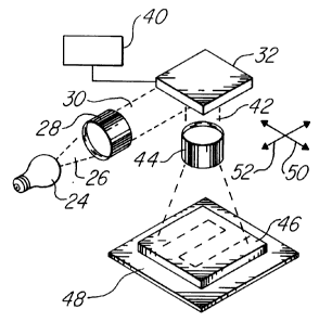
The present embodiment of the culTent invention is shown in Figure 2. The
layout data is entered into computer 40. Light source 24, which as an example may
be ultraviolet, produces rays 26 which are collected by lens 28, directed onto a spatial
light modulator 32 and generally brough to focsu at the aperture of imaging lens 44.
The spatial light modualtor by selectively addressing pixel elements, causes
TI-16846 5
2075026
individual portions of the illuminating beam 30 to be reflected into the lens 44 along
path 42. The spatial light modulator, in this embodiment, comprises individuallycontrolled elements, such as deformable mirror devices, as an example, or liquidcrystals may be used in embodimènts using light at other frequencies.
The selection of the individual elements of the array to reflect light is
completed by the computer 40 using the layout data. The computer cause~ the array
to form an image of the desired circuitry upon the member 46, which is a board
coated with resist, or a reticle substrate. In the fonner case, this accomplishes the
same step~ as discussed above, but eliminates the need for a master reticle and the
working film. The computer data file of the desired layout basically replaces the
master reticle as the source of the desired image. In the latter case, it is possible to
pattern reticle substrates in this manner also, for manufac~urers whose equipment
requires the use of reticles.
The member 46 rests upon a movable stage 48 or moving platform that can be
shifted in the x direction shown by arrow 50, and, independently in the y direction
shown by arrow 62. This allows the member to be aligned and passed under the
array to image the member correctly. The member is imaged in a mosaic fashion, as
opposed to a linearly scanned fashion, as is typically used with a laser scanner. The
member is repeatedly stepped by the computer controlled x-y stage, exposing one
block of the mosaic at a time, to the light from the spatial light modulator.
The board then undergoe~ the same processes as discussed above. If a problem
is found in the finished board, rather than redesigning the layout, manufacturing a
TI-16346 6
2075026
new master reticle and a new working film, all that is required i8 to correct the
design file and rerun the PCB. The new board can be made directly from the
corrected layout data, as it is used to control the spatial light modulator.
The spatial light modulator could be one of many types. In this embodiment
5 of the present invention, a deformable mirror device (DMD) i8 used. A side view of
one mirror element is shown in Figure 3. The DMD is typically manufactured
monolithically in ~ilicon as a linear or an area array, but only one element is shown
here. A substrate 54 is covered with metal and patterned to form the address
electrodes, not shown. A spacer layer 56 is then coated on the electrode layer. A
10 layer of thin reflective metal is then deposited on top of the spacer, followed by a
thick layer of the same or ~imilar metal 60. To define the mirror element 64, the
thick layer 60 is patterned and etched to leave the thick metal eve~rwhere but in thè
gaps 66 and over hinges 68. Holes 62 are left in the thick layer to allow undercutting
of the spacer layer 56. The resultant structure compnse~ mirror element 64
15 suspended over the air ~ap on hinges 68. When the electrode to either side of the
hinge centerline of the mirror on substrata 54 is addressed, the torque rotates the
mirror about the hinge, causing the light being directed onto the mirror to be
deflected along a different optical path. This architecture i~ know a~ the bistable
torsion beam DMD. Other configurations of the DMD could be used, including linear
20 and area arrays, and pixel element~ of differing sizes and geometric configurations.
Combinations of DMD~ could be used as well, to speed the proces~, or simply the
step-and-repeat patterns.
TI-16346 7
2075D26
Figure 4 shows an area array of the DMD device~. The substrate 54 show~
many reproductions of the nirror element, or cell, 64. The data can be loaded in any
number of ways to coincide with the desired pattern to be projected upon the imaging
member. One of those ways is sh`own by the arrows 70 and 72 in Figure 5.
The data is loaded serially into a row of cells, conceptually shown by arrow 70
. The line of cells containing mirror 64a corresponds to the line of image data 76 on
the member 46 in its initial star~ing place. A~ the data is passed in parallel down
the array in the direction of arrow 72 to the row of cells with 64b, the member moves
in synchronization with the line of data. The line of data 76 moves with the member
along direction to what had been position 78. Similarly, a~ the data move~ to the row
of mirrors with 64c, the board would move to force the line of data to be at what had
been position 80. The given line of information would expcse the same area on the
board for as many lines as the area array contains. By this method, a flow of the old
data acros~ the face of the chip is mirrored at the board at a constant location. The
result is a greatly improved exposure time for the photolithography proces~, and a
similar improvement in process speed.
The number of lines available in the ~patial light modulator array could exceed
the number of sequential exposure~ required to fully expose the photoreo.ist layer on
the PCB or the reticle substrate. The option then exists to te~ninate the parallel
flow of a particular line of data across the spatial light modulator array and reduce
the total light energy level impinging on the PCB or reticle. By controlling the total
number of exposure lineR actually utili~ed, the exposure process can be tailored to
TI-16346 8
, j
2075~26
accomrnodate process equipment and photoresist chemistry variables.
TI~