Note: Descriptions are shown in the official language in which they were submitted.
-1- 2075097
RECORDING APPARATUS,
RECORDING HEAD AND SUBSTRATE THEREFOR
FIELD OF THE INVENTION AND RELATED ART
The present invention relates to a recording
apparatus, a recording head usable therewith, and a
substrate for a recording head. The recording
apparatus is used as an output machine for a copying
machine, a facsimile machine, a word processor, a host
computer or the like. More particularly, it relates
to the same in which a plurality of recording elements
are used, which are selectively driven by integrated
circuit for the driving.
Various types of recording machines are
known. Among them, a liquid ejection recording
apparatus in which ink is ejected through ejection
outlets provided for the respective recording
elements, are desired because of the advantages of the
low noise non-impact recording operation, capability
of high density recording, capability of high speed
recording. The recent demands for such apparatus
includes the compactness and low cost.
Among the liquid jet recording apparatus, a
type using electromechanical converters (piezoelectric
elements, for example), a type using electrothermal
transducers and a type using pairs of electrodes
supplied with a voltage to eject liquid droplets, are
-2- 2075097
known. Further among them, an ink jet recording
apparatus of a type in which the recording liquid is
ejected using thermal energy, has been commercialized
because of its advantages that the liquid ejection
outlets (orifices) can be arranged at high density
with the result of capability of high resolution
recording and that the multi-nozzle (orifice).
arrangement is relatively easy with the result of
capability of the high speed printing.
In a known recording head used with the
recording apparatus of this type, a plurality of
recording elements are arranged in a line, and the
record~.ng elements are divided into plural blocks each
having several tens recording elements, and several or
several tens driving circuits for the respective
blocks, are formed on one substrate as integrated
circuits. The recording elements are selectively
driven in accordance with image data by the driving
circuits, so that the recording is effected on the
recording material such as paper.
These recording heads are particularly noted
because of its high resolution and high speed
recording. However, further reduction of the cost and
the size and the improvement of the performance, color
printing function, or the like are desired. Referring
to Figure 29, there is shown a conventional substrate
(heater board) having recording elements thereon and a
-3- 2075097
schematic sectional view of the ink jet recording head
using the substrate.
In Figure 29, (d), reference numeral 1
designates a heater board having thermal energy
generating means in the form of an electrothermal
transducers 2 a top plate 17 is provided with grooves
constituting a part of passages for ink 3. The ink 3
is supplied through the passages formed by the heater
board 1 and the top plate 17, as indicated by an arrow
A. The ink is then heated by the electrothermal
transducers 2 on the heater board 1 so that the ink is
ejected through the ejection outlets 5 in the
direction indicated by an arrow B. In Figure 29, (a)
- (c), show arrangements of various elements in the
heater board 1. It includes electrical leads for
electrically connecting various elements, diode arrays
7, and pads 8 for external electrical connection. In
the arrangement of Figure 29, (a), the electrothermal
transducers 2, the electrical leads 6, the diode
arrays 7 and the pads 8, are disposed in the order
named from the ejection outlet 5 side.
In Figure 29, (b), the electrical connection
between various elements are the same as in Figure 29,
(a), but the electrical leads 6 portion and the diode
array 7 portions are mixed. In Figure 29, (c), the
electrothermal transducers and the pads 8 are arranged
with one-to-one relation therebetween.
-4- 2075097
In an arrangement of Figure 30, (a), (b) and
{c), an ink supply port 9 is formed in the heater
board 1 having the electrothermal transducer, as
contrasted to the case of Figure 29. In this case,
the ink is supplied from the backside of the substrate
cover as indicated by an arrow A, and the ink is
ejected in a direction substantially perpendicular to
the surface of the substrate 1, as indicated by an
arrow B.
As for the wiring in the heater board shown
in Figure 29 or 30, two types are known. In one of
them, as shown in Figure 29, (c), and Figure 30, {a) -
(c), and Figure 31 designating the equivalent circuit,
the electric signals are supplied from the pads 8 to
the electrothermal transducers in one-to-one relation
(direct drive type). In the other type, as shown in
Figure 29, {a) and (b) and Figure 32 showing an
equivalent circuit, a matrix arrangement using diodes
are used, in which the electrothermal transducers are
selectively driven by selective drive voltage
application between segment pads SEG and common pads
(matrix drive type).
In the direct type shown in Figure 31, n pads
8 are required for n ejection heaters (electrothermal
transducers) 2. In addition, VH pad is required, and
therefore, (n+1) pads are required in total. Since
the pads 8 are directly connected to the ejection
2075097
-5-
heaters 2, a large current such as approx. 150 mA.
With a pulse width of 7 uS in a 360 dpi recording head
for plain paper according to an example of experiments
by the inventors, flows therethrough.- In addition,
the same current multiplied by n, flows through the VH
pad. Thus, all the electrical leads have to be
designed for large current. Because of the number and
large size of the pads, a large area is required for
the wiring with the result of bulky substrate and
recording head and high manufacturing cost. From the
standpoint of the main assembly of the recording
apparatus, the connecting portion and the wiring
therein are complicated due to the large number of the
pads.
Figure 32 shows another type of matrix drive
system. The number of electrical leads and the pads
is decreased as compared with the above-described
direct type. However, when n ejection heaters 2 are
used, the minimum number of pads is 2~ (when 2~ is
not an integer, the value is rounded, and added by 1)
are required at minimum. The electric current flowing
through the common electrode (COM) pad is the electric
current per one ejection heater multiplied by the
number of ejection heaters connected with the matrix,
as the case may be, and therefore, the electrical
leads 12 have to be designed for the large current.
Generally, in an ink jet recording head,
_6_ 2075097
there is a liability that the pressure wave at the
time of bubble formation is transmitted toward
upstream (toward a common liquid chamber) in the form
of a back wave, with the result of fluid cross-talk
among nozzles. Therefore, simultaneous drives of
adjacent nozzles may result in instable ejection due
to the back wave. In view of this, it is desirable
that the simultaneous drives are effected for nozzles
which are spaced greatly, from the standpoint of
stabilized ejection and high image quality. However,
in the case of the above-described matrix drive
circuit, if the common electrode simultaneously drives
a large number of different driving elements (COM),
large current flows through the thin segment (SEG)
leads with the result of potential difference within
the leads. If this occurs, the electrothermal
transducers are not supplied with proper electric
energy. For this reason, there is a problem that the
large number of elements are not driven.
The problem of the large number of pads and
the complicated wiring in the heater board, is more
significant in the case of color recording.
In order to accomplish the color recording,
the recording apparatus is provided with a plurality
of recording head for the respective colors.
Figure 33 is a block diagram of a circuit
structure for a conventional liquid jet recording
2075097
apparatus for color recording. Designated by
references 2C, 2Y and 2M are recording elements
(electrothermal transducers) for cyan, yellow and
magenta recording. Several tens of such elements are
used. Function elements 10 are for controlling power
supply to the recording elements. A shift register
circuit 11 aligns the image data, corresponding to the
recording elements. It is directly connected with a
latching circuit 12 storing data for the recording
elements. By using an output of an AND gate receiving
as inputs an output of the latching circuit and an
output of another AND gate connected at the input to
the signal lines 14 and 15 for controlling the power
supply period to the recording elements, the recording
element can be supplied with the power during the
output period of the first mentioned AND gate. In the
Figure, the zone indicated by the broken line is
formed on the substrate, and therefore, the
electrothermal transducers 2, function element array
(transistor array 10 in this embodiment) for
selectively driving the electrothermal transducers 2,
are formed on the substrate.
With this structure, however, the number of
contacts between the recording head carriage (main
assembly) and the electrical leads is still large with
the result of complicated driving circuit. Therefore,
the design and productions are still difficult.
2075097
_8_
U.S. Patent No. 5,030,971 discloses that in
order to reduce the size of the color recording
apparatus, the substrates for the different color are
made integral. In the U.S. Patent, the elements for
the four colors are formed on the same substrate. The
driving circuit in this patent is in the diode matrix
type, and therefore, the number of electrical.leads is
small as compared with the case of the direct driving
system, and therefore, the size of the recording head
itself can be reduced. This will be satisfactory if
the number of electrothermal transducers is small.
However, if the number is increased to meet the demand
for the high speed recording, for example, the number
of electrical leads and the pads increases
accordingly, with the result that the above-described
problem arises.
As regards the manufacturing of the
substrate, the yield decreases with increase of the
number of recording elements (electrothermal
transducers), since the number of diodes and
transistors also increases. Also, the yield in the
formation of the ink ejection outlets or the like by
connection with the substrate, and therefor, it has
been difficult to manufacture the substrate having a
large number of recording elements.
In the case of the substrate having the
supply port as shown in Figure 30, the utilization
2075097
_g_
factor of the silicone wafer constituting the
substrate can not be increased with the result of high
cost.
SUN~lARY OF THE I NVENT I ON
Accordingly, it is a principal object of the
present invention to provide a substrate, a recording
head using the same and a recording apparatus using
the same, in which the wiring on the substrate is
simplified.
It is another object of the present invention
to provide a substrate, a recording head using the
same and a recording apparatus using the same in which
a number of pads on the substrate is reduced, so that
a larger number of recording elements can be formed on
the substrate.
It is a further object of the present
invention to provide a substrate, a recording head
using the same and a recording apparatus using the
same, wherein even when a large current is used, the
current is not concentrated locally on thin electrical
leads.
It is a yet further object of the present
invention to provide a substrate, a recording head
using the same and the recording apparatus using the
same in which a number of electrical connection pads
is increased, so that the wiring can be simplified and
-10- 2075097
that the manufacturing is easy, the size is reduced
and the cost is reduced.
According to an embodiment of the present
invention, there is provided a substrate having plural
recording elements and electrical leads for supplying
electric signals to the recording elements,
comprising: electrical contacts for external
electrical connection for reception of image signals
used for driving the recording elements; and a
processing circuit for converting signals which are
serially supplied to the connecting contact to
parallel signals to be applied to the recording
elements.
According to another embodiment of the
present invention, there is provided an ink jet
recording head having a substrate with plural
recording elements and passages for supplying liquid
to a neighborhood of the recording elements, the
improvement residing in the substrate, comprising:
electrical contacts for external electrical connection
for reception of image signals used for driving the
recording elements; and a processing circuit for
converting signals which are serially supplied to the
connecting contact to parallel signals to be applied
to the recording elements.
According to a further embodiment of the
present invention, there is provided a recording
-11- 20~509~
apparatus for effecting recording operation with ink
droplets ejected, comprising: a recording head having
a structure defined above; and electrical signal
contact connected with the recording head to supply
the signal thereto.
These and other objects, features and
advantages of the present invention will become more
apparent upon a consideration of the following
description of the preferred embodiments of the
present invention taken in conjunction with the
accompanying drawings.
BRIEF DESCRIPTION OF THE DRAWINGS
Figure 1 is a top plan view illustrating an
example of layout on a substrate, according to an
embodiment of the present invention.
Figuxe 2 is a circuit diagram of an
equivalent circuit, according to an embodiment of the
present invention.
Figure 3 is a circuit diagram of an
equivalent circuit on a substrate, according to the
embodiment of the present invention.
Figure 4 is a drive timing chart according to
an embodiment of the present invention.
Figure 5 is a perspective view of a substrate
according to an embodiment of the present invention.
Figure 6 illustrates manufacturing process
-12- 2075097
for the substrate, according to an embodiment of the
present invention.
Figure 7 illustrates manufacturing process
for the substrate, according to an embodiment of the
present invention.
Figure 8 illustrates manufacturing process
for the substrate, according to an embodiment.of the
present invention.
Figure 9 illustrates manufacturing process
for the substrate, according to an embodiment of the
present invention.
Figure 10 is an exploded perspective view of
a recording head cartridge using the substrate of
Figure 1.
Figure 11 is a sectional view of the
substrate of Figure 10 around a nozzle.
Figure 12 is a sectional view of the
substrate of Figure 10 around a nozzle.
Figure 13 is a sectional view of a recording
head using the substrate of Figure 1.
Figure 14 is a sectional view of a recording
head using the substrate of Figure 1.
Figure 15 is a circuit diagram in a
conventional color recording apparatus.
Figure 16 is a drive timing chart for a color
recording apparatus to which the present invention is
applicable.
2075097
-13-
Figure 17 is a exploded perspective view of a
color liquid jet recording apparatus to which the
present invention is applicable.
Figure 18 is a circuit diagram of an
equivalent circuit capable of cascade connection,
according to an embodiment of the present invention.
Figure 19 is a top plan view of a substrate
capable of cascade connection, according to an
embodiment of the present invention.
Figure 20 is a perspective view of
semiconductor chips for a recording apparatus which
have been cascade-connected, according to an
embodiment of the present invention.
Figure 21 is a circuit diagram illustrating
the cascade connection in a color recording apparatus
to which the present invention is applicable.
Figure 22 is a timing chart for the circuit
of Figure 21.
Figure 23 is a perspective view of an
elongated semiconductor chip of a recording apparatus
according to an embodiment of the present invention.
Figure 24 is a perspective view of a
recording apparatus according to an embodiment of the
present invention, in which semiconductor chips are
cascade-connected in staggered manner.
Figure 25 is a perspective view of a
recording head using the substrate of Figure 24.
2075097
-14-
Figure 26 is top plan views of substrates
according to other embodiments of the present
invention.
Figure 27 is a perspective view of a
recording apparatus to which the present invention is
applicable.
Figure 28 is a perspective view of a.
recording apparatus to which the present invention is
applicable.
Figures 29 and 30 are top plan view of
conventional substrates.
Figures 31 and 32 are circuit diagram of
equivalent circuits thereof.
Figure 33 is a circuit diagram of an
equivalent circuit in a conventional color recording
apparatus.
DESCRIPTION OF THE PREFERRED EMBODIMENTS
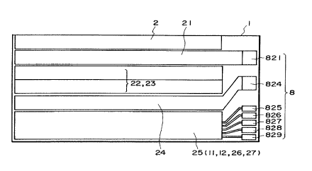
Referring to Figure 1, there is shown a
semiconductor chip 1, according to an embodiment of
the present invention. Recording elements are
arranged in the longitudinal direction of a substrate
1 in a recording element zone 2. Each of the
recording elements are connected to a common electrode
21 at the power supply side, by through hole.
Designated by reference numeral 821 is a power supply
pad {VH) for the recording elements. Function element
2075097
-15-
arrays 22 and 23 control the power supply to the
recording elements, and are arranged so as to permit
high density printing. Designated by reference
numeral 24 is common grounded electrode (GND) for the
recording current for the recording elements. The
area thereof is determined depending on the current
level supplied to the recording elements. Designated
by a reference numeral 824 is a grounding pad. One of
the features of the present invention is in a logic
circuit zone 25 in which there are provided a logic
gate zone 26, a latching circuit 12, shift registers
11 and 27 are formed on the surface of the
semiconductor chip in the form of a driving integrated
circuit. The logic circuit 25 functions tQ control
the function element arrays connected to the recording
elements (thermal transducer elements).
Figure 2 shows an example of an equivalent
circuit of the substrate having the structure as shown
in Figure 1. The recording element 2 is connected
with a transistor 23 for selecting the recording
element 2. There is shown an enabling leads (EI) for
actuating the recording element at a given timing, a
latch 12 for latching the printing data corresponding
to the recording elements, input leads (SI) for
receiving serial data and a shift register 11 for
shifting the serial data with predetermined timing.
Figure 3 is a further equivalent circuit of
20~g097
-16-
the equivalent circuit of Figure 2. The fundamental
circuit structure is the same as that shown in Figure
2, but in this circuit, the two enabling signal leads
are replaced by one lead.
Figure 4 is an operating timing chart of the
circuit of Figure 3. In Figures 3 and 4, recording
elements are indicated as n heaters R1 - Rn, as an
example. The circuit comprises a transistors 22,
logic gates 13, a latching circuit 12 and a shift
register 11. It further comprises pads 821 - 829
including the VH pad 821, GND pad 824, a strobe pad
825, a latch pad 826, a data pad 827, a clock pad 828
and logic power source VDD pad 829.
Referring to Figure 4, the operation of the
circuit of Figure 3 will be described.
Clock signals 18 and serial data signals 18
synchronized therewith are supplied to the shift
register circuit 11 at the timing shown in Figure 4.
When all of n data are set, a latch signal (negative
logic) 16 shown in Figure 4 is supplied to the latch
circuit 12, by which the supplied data are stored.
The data are kept stored until the next latching
signal is supplied. Then, an AND-output of the strobe
signal 14 and the latch output provided by the logic
gate 13 is supplied to the transistors 22 and 23, so
that the driving signals for the heaters R1 - Rn
(output signals of the transistors) are produced. In
2075097
-17-
this embodiment, the driving signal wave form is
determined by the input wave form of the strobe signal
13 (enabling signal (EI), in the case of Figure 2
example).
In the circuit of Figure 3, the output timing
of the driving signals for the heaters R1 - Rn, are
simultaneous in synchronism with the strobe signals
14. In the case of the timing chart of Figure 4, the
different timing is usable, when a delay circuit is
used as shown in Figure 18 which will be described
hereinafter.
As will be understood from Figures 1 - 4, the
minimum required number of pads for the heater board
is seven, irrespective of the number of recording
elements 2, in this embodiment. Therefore, the
complication of the electric wiring attributable to
the high density nozzle arrangement, can be avoided.
The following Table 1 gives the minimum
required pad numbers on the heater board in relation
to the number of ejection heaters, in various driving
systems.
_18_ 2075097
Table 1
No. of Min. Required No.
Heaters
(m)
Direct Drive Matrix Drive This Embodiment 1
8 9 6 7
16 17 8 7
64 65 16 7
4736 4737 138 7
As will be understood from Table 1, when the
number of ejection heaters 2 is larger than 16, the
number of pads is smaller in this embodiment than in
the direct driving system or in the matrix driving
system. The advantageous effect is even more
remarkable when the number of the heaters increases.
When a line head (covering A4 size with 400 dpi) is
considered, the number of nozzles is as large as 4736,
and therefore, the number difference between the prior
art system and the present embodiment system is
greatly significant.
Furthermore, in this embodiment, four pads,
namely the strobe pad 825, the latch pad 826, the data
pad 827 and the clock pad 828 among the seven pads,
deal with logic signals, and not in the power supply
line, and therefore, the large current does not flow
205097
-19-
therethrough. For this reason, the size of the
electrical leads may be small. The electrical leads
therefor can be arranged in smaller space. This
permits a larger size electrical leads for the power
supply for the heater. Accordingly, even upon the
electric current concentration occurred, the electric
power loss hardly occurs.
Referring to Figure 5, there is shown a
structure of the substrate of Figure 1 according to an
embodiment of the present invention. The basic
material of the substrate is usually silicon, but it
may be another material if a semiconductor can be
formed thereon. The substrate 1 comprises a basic
semiconductor layer 1029, and the semiconductive
element has been formed through known ion implantation
or the like. The semiconductive elements are
designated b~y reference numerals 1015, 1016, 1023,
1024, 1025 and 1026. On the semiconductor layer 1029,
a first electric insulating layer 1028 is formed, and
an electric conductive layer is patterned on the
insulative layer. The conductive layer is properly
contacted to the semiconductive layer 102 for
establishment of the circuit structure of Figures 2
and 3 via through holes (not shown).
The first conductor on the insulating layer
1028 includes VH leads 21 for supplying the electric
energy required for bubble creation of the liquid, GND
2075097
-20-
leads 24 for the electric grounding of the leads 21,
enabling leads 1019 for actuating the electrothermal
transducers 2 at given timing, latch leads 1020 for
latching the print data, serial data leads 1021 for
supplying the serial data and clock leads 1022 for
shifting the serial data at predetermined timing. On
the first conductor, there is provided a second
insulating layer 1027, and a second conductive layer
is provided thereon which is properly contacted via
through holes. To the ejection heater 2, the electric
energy is supplied through VH-heater lead 32 via a
through hole contact. The other end of the heater is
connected to a collector of a transistor 10 via
through hole of the first insulating layer and through
a heater-transistor lead 33. The first transistors 10
and the second transistors 10 are arranged in two
lines, but they are staggered to improve the area
factor.
When, for example, the heater arrangement
pitch is small, the transistor are arranged in plural
lines since the area factor is better if the
configuration of the transistor is close to right
square. The other end of the transistor 10 (base) is
connected to the logic gate 1023 via transistor base
line 28. The transistor base lead 28 is made of
polysilicon or the like. As for the first and second
conductive layer material, aluminum or other low
-21- 2075097
resistance material is used. The other end (emitter)
of the transistor 10 is connected to the GND lead 48
via through hole and through the transistor-GND line.
The logic gate 1023 selectively transmits ON-signal to
the transistor through the enabling line 1019.
Because of the driving nature of the enabling
line 1019, the electrothermal transducer elements 2
are independently actuatable. The current flowing
through the enabling line 1019 is very small, and
therefore, the power loss is small even if the wiring
thereof is complicated, and therefore, the ejection
heaters 2, can be selectively actuated.
Referring to Figure 6, an example of
manufacturing process of the substrate 1 shown in
Figure 5, will be described. This Figure illustrates
the process steps after the latching circuit 12, the
shift register circuit 11 and the transistors 10 and
the like have been manufactured through ion
implantation or diffusion. In Figure 6, designated by
(a) is a top plan view, and (b) is a partial sectional
view.
In this embodiment, the signal line for
actuating or deactuating the transistor by application
of logic signals from the shift register 11 to the
transistor 10, are provided by the semiconductive
layer. This is permitted because the electric current
between the shift register 11 and the transistor 10 is
207509 7
-22-
very small, and therefore, there is no need of
providing electric lines for this purpose.
Further, in the structure of the substrate of
this embodiment, the transistors 10 are staggeredly
arranged as shown in Figure 6(a) with alternatingly
different distances from the shift register, thus
increasing the pattern integration. In the case of
the substrate for the ink jet recording head or
apparatus, the electric current flowing to the
recording element through the transistor is large,
which requires large area transistors. However, from
the standpoint of high resolution recording, the
distance between adjacent recording element is desired
to be small. The staggered arrangement permits both
requirements. In this embodiment, the distances from
the shift register to the transistor is changed in two
steps, but a~larger number of steps is usable.
Figures 7, 8 and 9 show the manufacturing
steps, and the manufacturing steps proceeds in the
order of (a), (b) of Figure 7, Figure 8, Figure 9, (c)
and (d) of Figure 7.
In Figure 7, (a), Si02, SiN or the like
between-layers insulating film 29 is formed on the
substrate shown in Figure 6, and through holes have
been formed for the electric connection with the upper
layer.
In Figure 7, (b), the first lines are formed
2075097
-23-
with aluminum or the like for the VH common electrode
21, the grounding line 24, the logic line 31, for the
contact 30 or the like.
As shown in Figure 8 by (a),-(b), a second
Si02 or SiN (Si3N4) or the like between-layers
insulating film is formed on the first wiring layer,
and through holes are formed therein. On the. second
insulating film, a second aluminum layer is formed,
and is patterned, so that the electric connections
between the electrothermal transducers 2 and the VH
electrode and the transistors, and the pads, are
formed (Figure 9).
Subsequently, in order to avoid the short
circuit between electrodes through the ink, a
protection layer 36 is formed, as shown in Figure 7,
(c). On the protection layer, an anti-cavitation
layer 37 made of Ta or the like may be formed, as
shown in Figure 7, (d). The anti-cavitation layer 37
functions to protect the electrodes and the other
layers from cavitation liable to occur bubble creation
and collapse in the ink.
Referring to Figure 10, the description will
be made as to the structure of the ink jet head using
the heater board 1 described above. A top plate 4
includes n orifices 5 and grooves in communication
therewith, respectively, although not shown in the
Figure. When the top plate 4 is combined with the
2075097
-24-
heater board 1, n recording elements 2 correspond to
the respective grooves, and therefore, the respective
orifices, and in addition, the ink chamber is formed.
The electrical pads 8 are disposed in marginal
portions of two sides of the heater board 1. They are
connected to the external lines for reception of the
electric energy, and are connected therewith through
wire bonding, gang bonding, bumping, clamping or the
like.
The member constituted by the top plate 4 and
the heater board 1 is mounted on an ink container
cover 38. The ink container cover is combined with an
ink container case to constitute an ink container for
accommodating the ink therein. In the ink container,
an ink absorbing material may be contained to retain
the ink therein, although not shown. The ink is
supplied to the nozzle through an ink supply passage
of the ink container cover 39 through a bottom portion
of the recording element array 2 of the heater board
1. This is best seen in Figure 11 which is a
sectional view. The ink is supplied to the backside
of the heater board 1 adjacent the position where the
recording elements 2 are arranged, through the supply
passage formed in the ink container cover 39. Then,
the ink reaches to the surfaces of the individual
recording elements through the nozzles of the top
plate 4. Here, the ink is heated by the ejection
2075097
-25-
heater 2 so that a bubble is created. By the pressure
of the bubble creation, the ink is ejected out through
the orifices 5 onto the recording material to form
dots. As shown in Figure 12, the ink-is supplied to
the surface of the ejection heater 2, the droplet of
the ink 42 is ejected by the pressure resulting from
the bubble creation 41.
The ink supply around the backside of the
substrate at the position having the recording
elements, the non-uniform temperature distribution of
the substrate is decreased, thus stabilizing the
recording action. In addition, the distance between
the recording element position and the ink supply
chamber 43 can be decreased to the minimum, and
therefore, the ink refilling speed can be increased,
thus accomplishing the high speed response of the ink
ejection.
The back wave described hereinbefore can be
diffused firstly because the distance is short between
the bubble creating position {recording element
position) and the common chamber 43 position and
secondly because the diffusing rate of the
configuration of the passage to the liquid chamber 43
can be increased. Thus, the cross-talk attributable
to the production of the back wave between nozzles,
can be minimized. In order to assure these
advantageous effects, the recording elements are
2075097
-26-
preferably disposed within 1000 microns from an edge
of the substrate, and further preferably, it is within
300 microns. Here, the position of the recording
element is determined on the basis of -the distance
from an end of the common liquid chamber to the center
of the recording element in the direction along the
liquid passage.
In the foregoing embodiments shown in Figures
- 12, the ink jet recording head using the
10 substrate is of the type wherein the ink is ejected in
the direction substantially perpendicular to the
surface of the recording element.
Referring to Figures 13 and 14, there is
shown an example of the recording head in which the
ink is ejected in the direction parallel to the
surface of the recording element. Figure 13 is a
partial sectional view thereof, and Figure 14 is a
sectional view.
In the Figure, a top plate 4 having grooves
for constituting liquid passages 47 is joined with the
substrate 1. The ink is supplied to the liquid
passages 47 from the common liquid chamber 43, and the
ink is supplied to the orifice by capillary force.
The electric signals are applied to the recording
elements corresponding to the liquid passages 47, and
heat is generated by the corresponding recording
elements. Then, the ink is heated, and a bubble 41 is
2075097
-27-
created. Hy the pressure caused by the bubble
creation, the ink is ejected through the ejection
outlet 5. To the substrate according to this
embodiment, having the shift register, recording
electric signals are supplied through the wire bonding
pads 45 from a print board 46.
Figure 15 is a circuit diagram of the
recording head element substrate capable of color
recording, according to an embodiment of the present
invention. The recording elements 2C, 2Y and 2M are
for cyan, yellow and magenta recording actions.
Several tens of the recording elements are used.
Function element 10 are the same as described in the
foregoing. A shift register circuit 11 functions to
align the image data in relation to the recording
elements. It is directly connected with a latching
circuit 12 for holding the data for the recording
elements the strobe signal 14 is capable of
controlling the on-period for the recording element.
The signals 1034C, 1034Y and 1034M is capable of
activating independently the respective color function
element blocks. An output is provided from an AND
gate receiving the strobe signal 14 and the signal
1034C, 1034Y, 1034M. The output of the AND gate is
supplied to an additional AND gate, which also
receives an output of the latching circuit. The
output of the additional AND gate permits electric
-2$- 2075097
power supply to the recording element for the period
during the outputting time. According to this
embodiment, a small and low cost recording apparatus
can be achieved by forming plural color recording
elements on the semiconductor chip (substrate).
Figure 16 is a drive timing chart of a
recording apparatus according to the embodiment of the
present invention. One of the features of this
embodiment is that the image data for plural colors
are serially supplied at the time of the image data
signal (SI) supply. In other words, the image data
for plural colors are not separately supplied, but is
sequentially and serially supplied to a single image
data signal input terminal 17 for the cyan, yellow,
magenta (black may be added) colors. The serial image
data for plural colors are sequentially transferred in
the shift register 11 with the aid of transfer clock
{SCK), so that the image data for the plural colors
are aligned for one line of the recording elements for
the respective recording heads. The shift register 11
shown in Figure 15 is electrically connected with the
latching circuit 12 to permit electric power supply to
the recording elements in relation to the image data
for the one period of the latch pulse signal (LAT) 16.
Actually, the recording elements are driven
dividedly for the respective colors, in the periodical
time duration capable of driving the recording
ao~509
elements. The dividing operation is carried out in
response to enabling signals 1034C, 1034Y and 1034M.
By the use of this signal and the strobe signal 14 for
determining the driving period which i-s proper for the
respective colors (the actuating pulse widths matching
the respective recording elements), the recording
element blocks divided for the plural colors, can be
selectively driven with constant pulse widths during
the periodical time duration determined by the
latching pulses.
Because of the use of the drive timing
described above, even if the recording operation is
carried out in plural colors, there is no need of
providing respective signal lines for the colors, so
that the number of electrical leads and the number of
pads can be reduced. Therefore, the size and cost of
the recording head substrate and the recording head,
can be provided. In the foregoing description, the
case of three color recording is taken. However, the
similar driving method can be used for a larger number
of colors, or for mono-color recording.
In the case of the monochromatic recording,
the same structure as in the color recording is
usable. By doing so, both of the color recording
.operation and the monochromatic recording operation
are enabled only if the recording head is exchanged.
As regards the discrimination between the color
-30- 2075097
recording and the monochromatic recording, a
discriminating code may be provided in the serial
data, and the data is fed back from the recording
apparatus to the printer. It is a possible
alternative that the recording head may be provided
with a cut-away portion which is detected by the
printer.
Figure 17 shows an embodiment in the form of
a color recording head cartridge, in which the
advantageous effects of the present invention are best
used. A top plate 4 is provided with ejection outlets
5M, 5Y and 5C for magenta, yellow and cyan colors,
respectively and with grooves for constituting
passages connected therewith. A semiconductor chip
(substrate) 1 has plural recording elements, function
elements and driving integrated circuits integrally on
the surface thereof. The surface thereof is provided
with electric pads 8 for connection with the
respective color recording elements 2M, 2Y and 2C and
for connection with power source. The common chamber
39 for supplying the ink materials to the respective
ejection outlets, are divided in this example into the
common chambers 39M, 39Y and 39C, for the respective
colors. The ink supplying common chambers 39M, 39Y
and 39C are ink supply containers 40M, 40Y and 40C,
respectively. In this embodiment, the size and cost
are reduced. The fundamental mechanism and the
2075097
-31-
operation of the recording head of this embodiment is
the same as those of Figure 10 embodiment, and
therefore, the detailed description thereof is omitted
for simplicity. -
Here, an example of the recording head in
which the ink is ejected in the direction
substantially perpendicular to the surface of. the
recording element, is taken. However, this embodiment
is applicable to the recording head of the type shown
in Figures 13 and 14, in which the ink supply system
is divided for the respective ink colors.
In the embodiment, the elements for the
respective colors are formed on a single substrate for
the color recording head. However, plural substrates
may be cascade-connected to meet the color demand the
long recording head demand.
Figure 18 shows an equivalent circuit in the
wiring of the substrate which is cascade-connected
with another substrate. Figure 19 shows a substrate
having such a circuit.
As contrasted to the case of Figure 3, output
contacts 831 - 833 are provided for the cascade
connection for the latching circuit 12 and the shift
register 11, as contrasted to Figure 3 embodiment.
The substrate is connected with another substrate
through the output contacts. By doing so, plural
substrates may be driven by a data input signal
2p~5097
-32-
required for driving one element substrate. In this
case, to the driving operation is substantially the
same as in the foregoing embodiment.
Conventionally, in the case of the substrate
or recording head having a large number of recording
elements, the manufacturing cost is quite increased
for the purpose of increasing the yield. However,
according to this embodiment, the number of connecting
lines can be reduced even when plural substrates are
connected to increase the number of recording elements
into an elongated recording head as in a full-line
recording head, and the manufacturing cost and the
design and manufacturing easiness, can be maintained.
In Figure 19 embodiment, the number of output
contacts is larger than that in the equivalent circuit
of Figure 18. However, this results from having made
the strobe signal lines or the like common with the
other substrate. As to how many lines are made
common, it is determined in consideration of the
entire design of the recording head by one skilled in
the art.
Figure 20 shows an embodiment in which the
semiconductor chips or substrates as described
hereinbefore are cascade-connected in relation to the
colors, and still the high speed printing is possible.
THe connecting pads 8 of the semiconductor chips 1M,
lY and 1C for the respective colors, are cascade-
2075097
-33-
connected with connecting elements (or wire bonding or
the like) 49. Figure 21 shows a circuit diagram of
this structure. Basically the contacts for the power
supply are made common, and the signal-line contacts
are cascade-connected. The equivalent circuit for the
respective colors in this embodiment is substantially
the same as in Figure 15 embodiment, and therefore,
the detailed description thereof are omitted for
simplicity. When the cascade-connection is made, the
image data corresponding to the total number of
recording elements, are serially supplied for the
respective colors in the case of the color recording,
and in the case of the monochromatic recording, the
monochromatic data corresponding to the total number
of recording elements are serially supplied. Figure
22 is a drive timing chart for driving the recording
apparatus of~this embodiment.
When the semiconductor chip recording
elements are arranged in the staggered manner, a
higher speed and a higher density printing becomes
possible, as shown in Figure 20. The relaying member
or substrate is mounted on the substrate for
supporting the semiconductor chip. This structure is
advantageous in that when the recording element or the
semiconductor chip is damaged for one reason or
another, the semiconductor chip may be exchanged as a
unit.
2075097
-34-
With this structure, the maintenance free use
is possible. Since the recording elements
corresponding to a recording width for one line and
the function elements therefor and also the driving
integration circuit, are structurally formed on the
same substrate, so that the full-line recording
apparatus capable of high reliability, high density
and high speed, can be provided.
Figure 25 shows a recording head unit
provided by the connection of the substrates shown in
Figure 24.
Figure 23 shows non-full-line type recording
head, in which the recording elements corresponding to
several tens semiconductor chips, the function
elements and the drive integration circuits are formed
on the same substrate, and the recording elements are
grouped for the respective colors, and the respective
liquid chambers 43M, 43Y and 43C are formed. By doing
so, a color liquid ejection recording apparatus of
high reliability, high density and high speed
printing, can be provided. Designated by references
51M, 51Y and 51C are ink supply pipes for the magenta,
yellow and cyan ink materials. As described
hereinbefore, the liquid chamber may be separated for
the respective colors in the case where the plural
substrates are cascade-connected in a color recording
head. Although not shown the liquid chamber is not
2075097
-35-
divided and a monochromatic full-line liquid jet
recording apparatus may be provided.
Referring back to Figure 18 showing an
equivalent circuit capable of the cascade connection,
it is different from the circuit of Figure 3 in that
the Figure 18 circuit includes a delay circuit 48.
The delay circuit of Figure 18 will be described,
referring also to the timing chart of Figure 4.
Similarly to the foregoing embodiments, the
clock signals 18 and the serial data signals 17
synchronized therewith, are supplied to the shift
register circuit 11. When the plural heater boards 1
are cascade-connected. The number of clock signals 18
and the data 17 is the number of cascade connection m
multiplied by the number n of the heater on the heater
board. When all the data are set, the latching signal
16 is supplied to the latching circuit 12, so that the
data is held.
With this state, a strobe signal 14 is
supplied to the delay circuit 48. In the delay
circuit 48, the delay time can be set for the
respective heaters in relation to the input wave form
of the strobe signal 14. It produces logical product
of the delay wave form and the latching data signal.
The ejection heater receives the logical product
signal of the delay output and the enabling signal 15.
Where the plural substrates 1 are cascade-connected,
2p~5p97
-36-
the enabling signal is effective to select the
substrate 1 to be actuated by the signal, when only a
selected substrate is to be actuated.
In this embodiment, any delay can be selected
for the respective heaters by the addition of the
delay circuit 48. This produces the following
advantageous effects:
(1) Since the instantaneous current flow
decreases due to the decrease of the number of
simultaneously driven heaters, and therefore the
voltage drops through the VH and GND lines can be
minimized: and
(2) It is possible to provide such a delay as to
prevent the simultaneous actuation of adjacent
heaters, in consideration of the problem that when the
adjacent heaters are simultaneously driven in the ink
jet recording head, the fluid cross-talk problem or
the temperature rise might arise.
In this embodiment, the substrate 1 has a
built in delay circuit for determining the drive
timing, but the same advantageous effects can be
provided by using plural strobe signal contacts.
Referring to Figure 26, another embodiment of.
the circuit arrangement on the element substrate will
be described. In Figure 26, (a), the VH lines 54 and
the GND lines are disposed immediately behind the
electrothermal transducer element array 2, and they
2075097
-37-
are connected with minimum distance therebetween, and
therefore, the electric loss is minimum.
In the structure shown in Figure 26 by (b), a
top plate having passage constituting grooves is
bonded to the substrate, as described hereinbefore,
since the element substrate of this invention is
mainly used for ink jet recording head. In order to
enhance the contactness between the top plate and the
substrate, it is preferable that the flatness of the
surface of the substrate is high. In Figure 26, (b),
the intersection between first and second lines, occur
at a position away from the recording elements where
the high flatness is particularly desired. In the
arrangement shown in Figure 26 by (c), the VH line 21
is disposed closer to the substrate edge than the
recording element array, and therefore, the circuit
wiring is possible without necessity for the multi-
layer structure of the wiring. Therefore, the cost is
reduced. In addition, there is no fold-back wiring,
so that the arrangements around the recording elements
are more free, so that the width of the heater can be
increased. In the arrangement shown in Figure 26, by
(d), the GND line 5 is disposed adjacent the recording
element array 2 with the result of lower electric
loss .
Figure 27 is a perspective view of a liquid
jet recording apparatus IJRA to which the present
_38_ Zp75097
invention is applicable. It comprises a lead screw
5005 which is rotatable by the forward and backward
rotation of the driving motor 5013 through drive
transmission gears 5011 and 5009. A carriage HC is
engaged with the screw 5004 of the lead screw 5005.
The carriage HC is provided with an unshown pin. The
carriage is reciprocated in the directions a and b. A
sheet confining plate 5002 urges the sheet to a platen
5000 over the carriage movable range. A photo-coupler
constituted by elements 5007 and 5008 is effective to
detect a lever 5006 of the carriage HC in the range to
switch the rotational direction of the motor 5013.
The position detected by the photocoupler is a home
position. A supporting member 5016 supports a capping
member 5022 for capping the front side of the
recording head. A sucking means 5015 functions to
suck the air in the cap to suck out the ink from the
recording head through the ejection outlets and
through an opening 5023 of the cap. A cleaning blade
5017 is movable toward and away from the recording
head. These elements are supported on a supporting
plate 5018. Other forms of cleaning members are
applicable. A lever 5012 moves together with movement
of a cam 5020 engaged with the carriage to start the
sucking recovery operation. The driving force from
the driving motor is transmitted by way of known
transmitting means such as clutch or the like.
-39- 2 O , 5 ~ 9 7
In this structure, the capping, cleaning and
sucking operations are enabled when the carriage cams
to the home position zone by the operation of the lead
screw 5005. However, such operations may be carried
out at different timing.
In this embodiment, the recording head
cartridge is carried on the carriage HC. The.
recording head 5030 is separable from the ink
container 5031. As will be understood from the
foregoing description, the size of the recording head
can be reduced according to the present invention, and
therefore, the recording head can be easily mounted on
the carriage or the like. Since the function of
converting the recording signal from the serial signal
to the parallel signal, which has been allotted to the
main assembly of the printer, is now assigned to the
substrate of~the recording head, the recording
apparatus may have a simple structure. Since the
number of contacts for the signal supply in the
recording head is small, the wiring is simplified, and
the manufacturing steps are simplified. In addition,
the compact and low cost recording apparatus can be
provided.
In the recording head used with such an ink
jet recording apparatus, the recording head may be
exchangeable by the user or may not be exchangeable by
the user. With the embodiments of the present
-40- 2075097
invention, the number of electric contacts is small,
and the area occupied by the contacts is small. For
these reasons, the embodiments are particularly
advantageous in the case of the recording heads
capable of being exchanged by the users.
Figure 28 shows a full-line type liquid jet ,
recording apparatus. In this embodiment, the. number
of recording elements corresponding to several tens
semiconductor chips, the function elements and the
driving integrated circuits are formed on one
substrate. Four of such line recording devices are
used, corresponding to cyan, yellow, magenta and black
color printings. It is possible to effect high
quality full-color recording. A pair of rollers 201A
and 2018 are provided for feeding the recording
material R in the sub-scan direction Vs. Full-line
type recording means 202BK, 202Y, 202M and 202C have
ink ejecting nozzles over a range corresponding to the
entire width of the recording material R. They are
arranged in the order of black, yellow, magenta and
cyan from the upstream side of the recording material
feed. An ejection recovery means 200 is faced to the
recording means in place of the recording material R
during the ejection recovery operation, and it
includes a cap, ink absorbing material, a wiping blade
or the like.
The typical structure and the operational
-41- 20~509~
principle are preferably the ones disclosed in U.S.
Patent Nos. 4,723,129 and 4,740,796. The principle and
structure are applicable to a so-called on-demand type
recording system and a continuous type recording
system. Particularly, however, it is suitable for the
on-demand type because the principle is such that at
least one driving signal is applied to an
electrothermal transducer disposed on a liquid (ink)
retaining sheet or liquid passage, the driving signal
being enough to provide such a quick temperature rise
beyond a departure from nucleation boiling point, by
which the thermal energy is provided by the
electrothermal transducer to produce film boiling on
the heating portion of the recording head, whereby a
bubble can be formed in the liquid (ink) corresponding
to each of the driving signals. By the production,
development and contraction of the the bubble, the
liquid (ink) is ejected through an ejection outlet to
produce at least one droplet. The driving signal is
preferably in the form of a pulse, because the
development and contraction of the bubble can be
effected instantaneously, and therefore, the liquid
(ink) is ejected with quick response. The driving
signal in the form of the pulse is preferably such as
disclosed in U.S. Patents Nos. 4,463,359 and 4,345,262.
In addition, the temperature increasing rate of the
heating surface is preferably such as disclosed in U.S.
-42- ~ 7 5 ~ 9 7
Patent No. 4,313,124.
The structure of the recording head may be as
shown in U.S. Patent Nos. 4,558,333 and 4,459,600
wherein the heating portion is disposed at a bent
portion, as well as the structure of the combination of
the ejection outlet, liquid passage and the
electrothermal transducer as disclosed in the.above-
mentioned patents. In addition, the present invention
is applicable to the structure disclosed in Japanese
Laid-Open Patent Application No. 123670/1984 wherein a
common slit is used as the ejection outlet for plural
electrothermal transducer, and to the structure
disclosed in Japanese Laid-Open Patent Application No.
138461/1984 wherein an opening for absorbing pressure
wave of the thermal energy is formed corresponding to
the ejecting portion. This is because the present
invention is~effective to perform the recording
operation with certainty and at high efficiency
irrespective of the type of the recording head.
The present invention is effectively
applicable to a so-called full-line type recording head
having a length corresponding to the maximum recording
width. Such a recording head may comprise a single
recording head and plural recording head combined to
cover the maximum width.
In addition, the present invention is
applicable to a serial type recording head wherein the
d 7 5 ~ 9 7
recording head is fixed on the main assembly, to a
replaceable chip type recording head which is connected
electrically with the main apparatus and can be
supplied with the ink when it is mounted in the main
assembly, or to a cartridge type recording head having
an integral ink container.
The provisions of the recovery means, and/or
the auxiliary means for the preliminary operation are
preferable, because they can further stabilize the
effects of the present invention. As for such means,
there are capping means for the recording head,
cleaning means therefor, pressing or sucking means,
preliminary heating means which may be the
electrothermal transducer, an additional heating
element or a combination thereof. Also, means for
effecting preliminary ejection (not for the recording
operation) can stabilize the recording operation.
As regards the variation of the recording head
mountable, it may be a single corresponding to a single
color ink, or may be plural corresponding to the
plurality of ink materials having different recording
color or density. The present invention is effectively
applicable to an apparatus having at least one of a
monochromatic mode mainly with black, a multi-color
mode with different color ink materials and/or a full-
color mode using the mixture of the colors, which may
be an integrally formed recording unit or a combination
-44- ~ 7 5 ~ 9 7
of plural recording heads.
Furthermore, in the foregoing embodiment, the
ink has been liquid. It may be, however, an ink
material which is solidified below the room temperature
but liquefied at the room temperature. Since the ink
is controlled within the temperature not lower than 30
°C and not higher than 70 °C to stabilize the. viscosity
of the ink to provide the stabilized ejection in usual
recording apparatus of this type, the ink may be such
that it is liquid within the temperature range when the
recording signal is the present invention is applicable
to other types of ink. In one of them, the temperature
rise due to the thermal energy is positively prevented
by consuming it for the state change of the ink from
the solid state to the liquid state. Another ink
material is solidified when it is left, to prevent the
evaporation ~of the ink. In either of the cases, the
application of the recording signal producing thermal
energy, the ink is liquefied, and the liquefied ink may
2~ be ejected. Another ink material may start to be
solidified at the time when it reaches the recording
material. The present invention is also applicable to
such an ink material as is liquefied by the application
of the thermal energy. Such an ink material may be
retained as a liquid or solid material in through holes
or recesses formed in a porous sheet as disclosed in
Japanese Laid-Open Patent Application No. 56847/1979
-45- ~ 7 5 ~ 9 7
and Japanese Laid-Open Patent Application No.
71260/1985. The sheet is faced to the electrothermal
transducers. The most effective one for the ink
materials described above is the film boiling system.
The ink jet recording apparatus may be used as
an output terminal of an information processing
apparatus such as computer or the like, as a copying
apparatus combined with an image reader or the like, or
as a facsimile machine having information sending and
receiving function.
As described in the foregoing, the ejection
heaters, function elements and integrated circuits for
selectively driving the function elements in response
to the serial image data, and electric contacts for
the external electric connection, are formed on one
and the same substrate, and therefore, the electrical
lead arrangement is not complicated even in a high
density multi-nozzle structure. Because of the small
number of contacts, the size of the head is reduced,
and the reliability is increased. Also, it becomes
easier to mount the substrate on the recording means
or apparatus, and therefore, the cost is reduced.
In the recording head of the type which can
be exchanged by the users, the advantages of the small
size and the mounting or demounting reliabilities, are
significant. According to the embodiments of the
present invention, the fluid loss is reduced, and the
-46-
utilization factor of the chip area is improved. In
addition, the reliability of the electric contacts in
the structure of using plural chips, is enhanced.
Furthermore, the time series drive control for the
purpose of avoiding fluid cross-talk peculiar to the
ink jet printing, can be made easier.
According to the present invention, a great
number of nozzles such as 18 - several 1000 nozzles
can be driven with the small number of electric
contacts (8 at minimum), and there is no limit for the
time shared drive. By the cascade connection of
plural chips arranged in the longitudinal direction of
the nozzle arrangement, the density of the recording
elements can be enhanced significantly. Since the
electric contacts do not obstruct the other
arrangement, the chip may be disposed close to the
electrotherm~l transducer element side or the opposite
side therefrom. Since the electric contacts may be
disposed at the opposite sides of the electrothermal
transducer elements, and the wiring resistance can be
minimized.
Since the shift register and or the driver
transistor or the like which have been disposed
conventionally away from the substrate, may be built
in the substrate, by which the resistance of the leads
can be minimized. Thus, the energy loss can be
reduced. Particularly in the case of the ink jet
2075097
-47-
system, the driving current is as large as several
hundred mA due to the principle of the bubble ejection
requiring bubble creation, the present invention is
advantageous. When the apparatus is driven by
buttery, the advantageous effects of the present
invention are also significant.
While the invention has been described with
reference to the structures disclosed herein, it is
not confined to the details set forth and this
application is intended to cover such modifications or
changes as may come within the purposes of the
improvements or the scope of the following claims.
20