Note: Descriptions are shown in the official language in which they were submitted.
~7~
I/O CONTROLLER APPARATUS AND METHOD FOR TRANSFERRING
DATA ~ETWEEN A HOST ~ROCESSOR AND MULTIPLE I/O UNITS
L~Q~n~
This invention relates to a computer method
and apparatus or transferring data ~etween a
processor section, i.e. a hos~ processor, and an I/O
section, i.e. one or more peripheral units or
input/output units.
More particularly, this invention provides
an I/O controller that can transfer multiple-byte
blocks of data, in what is known as a direct memory
access (DMA) transfer, and that can execute a
processor commanded transfer, designated a PIO
transfer, with high time efficiency.
I/O controllers are known for providing both
processor commanded transfers, i.e. PIO transfers,
and multiple-byte block transfers, i.e. DMA
transfers. Xn general, a PIO transfer is executed in
response to a command from the local processor in the
I/O controller and transfers a word or other unit of
information between the local processor and a
designated I~O unit. The esecution of a PIO transfer
typically i~ brief, for ezample requiring
appro~imately five microsecRnds ;n a ~ys~em~
operating with a si~teen megahertz clock. A direct
memory access transfer, on the other hand, transfers
a significantly larger quantity of data, typically
designated as a block having a specified number of
bytes, between the main storaqe unit of the host
~ 2 2~7~ 9
processor and a designated I~O unit. DMA transfer
rates are appro~imately our megabytes per second in
systems operating with a si~teen megahertz clock.
It is desirable, for time-wise efficient
operation, i.e., a high system speed, that DMA
tran~fers be e~ecuted promptly. It likewise is
desirable that PIO transfers be executed promptly.
In addition, ~t is preferflble that PIO transfers are
e~ecuted immediately, without waiting for the
completion of dn in-process DMA transfer, which could
take several milli~econds. For esample, if a DMA
transfer were underway to one disk drive address,
this could hold up a pending PIO to another disk
drive address. For e~ample, if the main system
directed an I/O controller to send a command to
another di~k drive, the ~/O controller would have to
wait until the end of the DMA transfer. At the same
time, however, it is inefficient to abort a DMA
tran~fer in order to accommodate a PIO transfer and
then require restarting of the same DMA transfer.
Among thea known I/O controllers that handle
both DMA transfers and RIO transfers are the model
XA2000 computer systems of Stratus Computer, Inc.,
and the techniques disclosed in U.S. Patents Nos.
4,926,315; No. 4,~09,754; and No. 4,371,932. The
noted U.S. Patent No. 4,371,932 provides an
interleaving mechanism that enable host processor
dir~ct program control data transfers to be performed
on a cycle steal basis when the I/O controller is
executing data transfers for a block of data. The
patent describes ~ ~ual port random access storaqe
mechanism to provide temporary storage in e~ecuting
the DMA and the PIO data transfers.
- : , .
,. ~
2 ~ 7 ~
--3--
It i~ an object of this invention to provide
an improved method and apparatus for the transfer,
between a ho6t processor and multiple I/O units in a
digital data processing system, of data on both a
direct memory access basis and a processor command
basis with high time-wise effic~ency.
Another object is to provide such a method
and apparatus for providing both DMA and PIO
trans~ers with minimal wait for PIO transfers and
minimal delay for DMA transfers.
It is a further object of the invention to
provide an I/O controller that interleaves PIO-type
trans~ers with DM~-type transfers with minimal delay
for both kinds of transfers.
Other objects of the invention will in part
be obvious and will in part appear hereinafter.
Summary Of the InventiQn
An I/O controller according to the invention
responds to a request or a processor commanded data
(PIO) transfer, during the execution of a direct
memory access-type (DMA-type~ transfer, ~y idling the
DMA transfer without a change in its active status,
executing the PIO transfer and then resuming th~ DMA
transfer at the same point it was idled.
The controller employs control and status
hardware to attain the idling and subsequent
resumption of the DMA transer with minimal added
operational time.
~::
-4- 2~7~
The 1/0 controller attains this operation in
part by the storage of ~ta~us information regarding
the DMA transfer in process, and the updating of that
status information, and further by maintaining the
system components involved in the DMA transfer in the
same ~tate of readiness to perform a DMA transfer
both during the idling for an intervening PIO
transfer as during the actual execution of the DMA
transfer.
An I~O controller according to the invention
has a local processor operating wi~h a local storage
unit, i.e. addressable memory, and transfers data
between a host processor having a host memory and a
peripheral device, i.e. an I/O device, on both a
direct memory access (DMA) basis and on a processor
command (PIO) basis. The I/O controller also can
scan the status of each of multiple peripheral
devices for interrupts. The I/O controller provides
these transfers and the scan operation with a high
level of ~ime effiGiency.
~ he I/O controller has a ~irst data-transfer
circuitry -- for e~ample a DMA Engine -- and has a
second data-transfer circuitry - ~or e~ample an I/O
bus control unit - that together move data during DMA
transfers without control by the local processor,
after being initialized and enabled for execution of
a DMA instruction. The local processor accordingly
is available to perform other tasks during ~MA
transfess.
., ~
.. . .
.. ..
.: . . : : :
` 2~37~9
'The local processor can suspend a DMA
operation to e~ecute a PIO operation, thereby
avoiding operating delays that would otherwise result
by requiring the PIO operation to wait. Moreover,
the DMA Engine can r~sume a suspended DMA operation
at the p~int of suspension, thereby avoidinq
operating delays that otherwise would result from
having to re-initlate the DMA operation.
In ~ccordance with another aspect of the
invention, the DMA Engine operates with a table for
storing information associated with a DMA instruction
and for countin~ the bytes of in-process DMA
transfers. The DMA ~able is undisturbed when the DMA
operation is suspended, thereby ma;ntaining intact
the contents of the DMA table.
The DMA table directs the DMA Engine for
each byte to be transferred, in a manner that enables
the DMA Engine to be ~u~pended and be resumed, i.e.
re-enabled or re-selected, repeatedly during a DMA
operation with a minimum of restart or other
house-keeping or overhead operations.
In another aspect, the DMA Engine contains a
countPr or the DMA byte~ beinq transferred during a
DMA operation. The counter i~ inactive during a
de-select of the DMA ~ngine, and active during DMA
tran~fers. ~ DMA Engine can, in this aspect, be
stopped in the midst of a DMA transfer and then
restatted at the point at which it was stopped. The
data moved for a qiven D~A tr~nsfer can then be
fini~hed without redundant or other repeated
maneuvers.
- , ,
,.
2~7~
. .
In another aspect, the DMA Engine can store
selective in~ormation to execute a DMA transfer. In
an illustrative instance, it can designate the
completion state of a given DMA transfer, for example
whether or not the DMA transer was completed or
whether an error exists in the ~ata that was
transferred.
According to further a~pects of the
invention, the I~O controller stores a li~t of
potentially ~ecut~ble, or candidate, DMA
instructionæ. The DMA Engine accesses the list
through a pointer set by local processor. The DMA
Engine monitors, in a ROLL state, a DMA instruction
as inde~ed by the pointer, If the DMA instruction is
executable, the DMA Engine processes the DMA
instruction and increments the pointer to the ne~t
DMA instruction within the list. I~ the DMA
instruction is not e~ecutable, the DMA Engine
continues to scan that DMA instruction through
successive IDLE and POLL states, until the DMA
instruction becomes esecutable. At the end of the
DMA Instruction List, the DMA Engine is incremented
to loop to the ~sginnin~ of the list to POLL the
~ir~t DMA instruction.
The DMA instru~tions in the list are written
from the local processor, which in addition specifies
with a GO code that a DMA instruction is ready for
~ecution. The GO code can be written to a DMA
instruction ~ven while the DMA Engine scans the entry.
:
. ~
2 ~ 7 ~
--7--
If, at any point in the DMA Instruction
List, ~he ~MA Eng~ne has returned to the same
instruction and does not PO~L an executable entry,
the DMA Engine waits at that location within the list
until the local processor makes another entry ~nto
the DMA Instruction List. When the local proce~sor
makes another ~ntry ~nto the list, the DMA Engine
again enters the POLL/IDLE ~tates, and resumes
~canning the DMA instruction.
In another aspec~, the I/O controller of the
invention provides a ~ual port storage ram to receive
and ~tor~ information rom the local processor, and
to store the list of candidate DMA instructions. The
storage ram is co~pled to a clocking arranQement
which prevents access conflicts, and in particular
Write conflicts, between the local processor and the
DMA Engine.
In yet another aspect, the I/O controller
employs a WRITEPIPE buffer arrangement between the
local processor and the data writing operations of
the I/O processor. This loqic arrangement removes
the inherent delays present in the host bus due to
the overhead operations of the local processor and of
Write operations associated with the DMA Engine.
In still another aspect, the I/O controller
employs a CHECKSUM ~torage operation, which is
selectable through the I/O controller, and which
stores the arithmetic sum of the bytes transferred
across the I/O bus. CHECKSUM operations are useful
in monitorin~ the byte content during multiple
transfers of data, ensuring that all bytes are moved.
:, ,,
2~7~
-B-
.
According to still another aspect of the
invention, di~ital logic apparatus is provided for
transferrinq multiple bytes of information, and for
communication with a host processor and a host
memory. The apparatus includes storage for a DMA
Instruction List, and DMA Engine logic circuitry to
interface with the DMA Instruction List. During
~uccessive IDL~/POLL states, the DMA Engine scans a
candidate DMA instruction within the list for a code
indicating an executable DMA instruction. If an
esecutable DMA instruction is found, the DMA Engine
processes the instruct~on and scans the next entry
within the list. ~he DMA Engine loops to the start
of the list after e~ecuting the last entry in the DMA
Instruction ~ist. If the DMA Engine overtakes the
list and does not find an e~ecutable ~ntry, the DMA
Engine waits for the local processor to write into
the list of candidate DMA instructions. Once an
entry is made, the DMA En~ine resumes its scan of the
DMA instruction.
The digital logic apparatus has another
aspect including sequence control logic. When the
DMA Engine i~ in successive I~LE and POLL states, the
DMA Engine scans a DMA instruction for a code
indication an e~ecuta~le in~truction. After an
executable DMA ~nstruction ig ~elected, the DMA
Engine loads ~ertain information about the DMA
instruction into the DMA Engins counters. In one
illu~trative ~mbodiment, this i~formation includes:
PKADR, 6pecifying the bus slot and the
~ource/destination address on the I/O side of the DMA
transfer; BCOUNT, ~pecifying the data type and bytP
count of the DMA tran~fer; and MEMADR, specifying a
location in system memory for the DMA transfer.
- - ~
9 2~7~
In add;tion, the DMA logic circuitry begins
a logical data-move operation for the selPcted DMA
instruction. If the DMA Engine is writing to an I/O
device, the DMA Engine reads data from the host
memory. If, on the other hand, the DMA Engine is
reading ~ata, the DMA ~ngine fills an available
buffer. When the bu~fer ~s full, the data is written
to the host memory until tha byte count is zero.
According to this aspect, a completion
status is written into the DMA Instruction List
denoting that either the DMA transfer was completed
or that an incorrect type of data or memory address
was specified. At that point, the latest DMA
transfer i5 cleared, the pointer which points to the
current location in the DMA Instruction List is
incremented, and the DMh Engine resumes operation in
its IDLE and POLL states.
In a further ~spect of the invention, the
digital logic apparatus includes CHECKSUM logic.
Thi logic, when ~elected, writes information
regarding the data bytes of a DMA transfer into the
current DMA transfer instruction.
According to another aspect of the
invention, a DMA Engine contains a counter that is
selectively deartivated by a priority operation of an
I/O controller. Upon the completio~ of A pri4rity
operation, the DMA Engine and counter resume - at the
point of interruption ~ the DMA transfer.
, ~
,
2~7~
--10--
The advantages of an I/0 controller having
th~ ~oregoing features are several. First, such a
DMA Engine can be temporarily stoppe~ and restarted
without redundant data transfers or losses of DMA
status. In addition, the rslatively small data
transfers of PI0 commands can be ~fficiently
prioritized over DMA transfers, which can involve the
time-consuming transfer of large blocks of data.
Further, the operations performed by the CPU, the DMA
Engine, and the Scanner remain uninhibited even with
the as~ertion o~ a PI0 command. Each continues to be
rea~y to operate as thouqh no priority assertion had
occurred.
These and other aspects of the invention are
evident in the drawings and in the description which
follows.
~rief_PescriDtion of ~he Drawi~g~
The foregoing and other objects of the
invention, the various features thereof, as well as
the invention itsel, may be more fully understood
from the following description, when read together
with the accompanying drawings in which:
FIGURE 1 is a schematic block diagram of a
digital data processing system utilizing an I~0
controller constructed in accordance with the
invention;
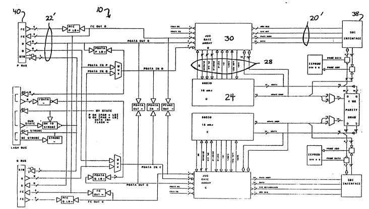
- FIGURE 2 illustrates an I/0 controll~r for
use in thP system of FIGURE 1, and showing various
data paths;
. : .,-. : ,
.
2 ~
~ IGURE 3 shows Gate-Array logic for u~e in
the I/O controller of FIGUR~ 2;
FIGURE 4 shows a DMA Engine for use in the
I/0 controller of FIGURE 2;
FIGU~E 5 shows a flow diagram illustrating
operation of the DMA ~ngine of FIGURE 4;
FI~URE 6 ~hows a flow diagram illustrating
operation of the PBUS Controller logic shown in
F I GURE l;
FIGURE 7 shows a flow chart illustrating
operation of the Scanner depicted in FIGURE 1: and
FIGURE 8 shows a cycle interleave chart
illustrating operation of the PBUS Controller logic
shown in FIGURE l.
Description of Illu~ated Embodiments
FIGURE 1 shows a block diagram of a digital
data processing system utilizing an I/O controller 10
in accordance with the invention. The system
depicted includes a host processor 12 coupled to a
host memory 14, an I/O controller 10, ana a multitude
of I/O units 15-18. The host processor 12
commun;cates to the ~everal I~O units 15-18 through a
host bu~ 20 that is ~onnected to the I~O controller
10, and through an I~O ~us 22 that is connected
between the controller 10 and the various I/O uni~s
15-lR. The I/O controller has a host bus estension
20' and an I/O bus e~tension 22~.
The I~O co~troller 10 operates with a local
processor 24~ such as a Motorola MC63030 32-bit
microprocessor, and a local random access memory 26.
: ~ ~ ,. " . ' . . ,
.... . .
-12- ~7~9
The microprocessor 24 communicates between the host
processor 12 and the ~everal I/O devices 15-18
through a local processor bus 28. The Gate-Array 30
in the controller 10 provides the interface path
between the local processor bus 28, the host bus 20
and the extension 20', and the I/O bus 22 and
extension 22'. There are two mechanisms for
transferring data through the I/O bus, a DMA (direct
memory access) transfer, consiæting of large bloc~s
of data, and a PIO (peripheral I/O command) transfer,
consisting of relati~ely small amounts of data, for
example one to four bytes per access.
The illustrated Gate-Array 30 has a first
data-transfer co-processor 32, for example a DMA
Engine, for transferring DMA ~ata between the I~O bus
22 and the estension 22', and either the local
processor bus 28, or the host processor bus 20 and
the e~tension 20'. The Gate-Array 30 has a second
data-transfer co-processor 34, namely, a P~US
Controller, for enabling the transfer of PIO data by
the local processor 24 through the I/O bus 22 and the
extension 22'.
.
The first data-transfer logic circuitry 32
is hereinafter referred to as a ~DMA Engine~, for
clarity of the description. Although certain
features o~ the Gate-Array 30 can be attained with a
conventional DMA Eng;ne, a DMA Enqine 32 as ~escribed
below ~mbodies ~urther features of the invention and
is preferred.
;
: : . ;, ' ~ ,. ~ : .
.,
. . .
~ ~7~
-13-
The I/O controller 10 thus provides
substantially separate logic circuits for DMA
transfers and ~or PIO transfers. The DMA Engine 32
provides the former and the local processor 24
provides the latter. Both the local processor 24 and
the DMA Engine 32 communicate with other elements of
the controller 10 and with the buses 20 ~nd 22
through the PBUS Controller 34 within the Gate-Array
30.
Other logic circuitry in the Gate-Array 30
and associated with the PBUS Controller 34 provides a
de-selection and re-selection capability of the DMA
Engine, whereby the logic circuits of the DMA Engine
32 can be temporarily frozen in the midst of a ~MA
transfer. This suspension of the DMA ~ngine allows
the PBUS Controller 34 to process a priority data
transfer, e.g., a PIO data transfer. The I~O
controller 10 thu~ enables the local processor 24 to
give priority to PIO data trans ers in favor of DMA
transfers. In this operation, the ~ate-Array 30
suspends and thereby stops any DMA transers in
progress, performs the PIO access, and then resumes
the ~MA transfer where it left off, with no loss of
data and with only few redundant or repeated
operations.
In addition, the illustrated I/O controller
10 has a Scanner 36, which is also linked to the PBUS
Controller 34. The illu trated Scanner 36 is a
separate logic unit for seanning the several I~O
units 15-18 for pending interrupts. The illustrated
Scanner 36 contains a register of four long-words for
~toring the interrupt ~tatus information ~f the
several I/O uni~s during a scan. In a preferred
.
,...
~7~
-19-
embodiment, as $11ustra~ed, the Scanner 36 does not
acce~s the I/O bus 22 for conducting a Scanner cycle
~f either a DMA transfer or a PIO transfer is in
progress.
The I~O controller 10 thsrefore dictates
priority acces~ r~que~ts, giving highest priority to
the local processor 24 and related PIO transfers,
ne~t priority to DMA Engine 32 accesses, and lowest
priority to 8c~nner 36 cycles. Accordingly, the
local processor 24, the DMA Engine 32, and the
Scanner 36 access the ~/O bu~ 22 as though each were
non-interruptable. The DMA Engine, however, is
suspended or frozen during higher priority operations.
Scanner 36 cycles are released only when they do not
conflict with PIO transfers and with DMA transfers.
A more complete operational understanding of
the I/O Controller 10 may be obtained by the
following description, together with reference to
U.S. Pat. No. 4,926,315, the teachings of which are
incorporated herein by reference. That patent
discloses a prior I/O controller of the assignee
hereof. For e~ample, a preferred embodiment of the
I/O bus 22 is a fault-tolerant, multiplexed and
burst-mode bus providing (n) datums ~or only one
address transfer, where (n) is a positi~e integer, as
described in U.S. Pat. No. 4,926,315.
FIGURE 2 ~hows urther detail of the I/O
controller 10 and ~hows data paths and control
connections between the several major components.
The illustrated local processor 24 is an MC68030 chip
operating ~t 16MHz. The processor 24 is linked to
, ~ ~
~ 2~7~9
-15-
the Gate-Array 30 vla the local processor bus 28,
which contains ~everal control lines. The ~ate-Array
30 is the $nterface element between the host
processor 12 (FIGURE 1~, connected ~ia the host bus
e~tension ~0' and thc ho8t bus 20 (FIGUREl), the
several I/O units, connecte~ through the I/O bus
e~tension 22' and the I/O ~us 22 (FIGURE 1), and the
local processor 24, connected through the local
processor bus 28. An interface ~tage 38 connec~s to
the host bus 20 and the ho~t bus extension 20', which
connects to the Gate-Array 30. An interface ~tage 40
connects to the I/O bus 22 and the I/O bus estension
22', which connects to the Gate-Array 30.
The controller 10 is shown in FIGURE 2
connected with an identical controller, in the same
manner set forth in the above-noted U.S. Patent No.
4,926,315, for fault toleran~ operation with that
second controller. Data comparison circuits are
connected between the two processors, for
error-checking purpoæes. Further, as also known, the
two processors are connected with a ~lash bus. This
showing in FIGURE 2 is illustrative of a specific
preferred embodiment, and the invention is not ~o
limited,
FIGURE 3 shows the Gate-Array ~0 of FIGURE 1
and several data paths within. The DMA Engine 32,
the PBUS Controller 34, and the Scanner 36 ~unction
within the ~ate-Array 30. The left side 41 of ~IGURE
3 shows data paths of the loc~l processor hus 28,
which conn~ct~ to the local processor 24. The lower
right portio~ 42 o~ FIGURE 3 ~hows data paths o the
,
',: ~ :
~ .
~ 2~7~9
-16-
I/O bus estension 22~. The upper right portion 43 of
FI~URE 3 shows data paths of the host bus e~tension
20 ' .
The DMA Eng~ne 32 is a data-moving
co-processor that resldes within the Gate-Array 30.
It processes DMA instructions as indexed by a pointer
receive~ from the local processor. This pointer is
Read/Write accessible by the local processor. The
~llustrated DMA Instruction List 44 is a memory
element within the Cate-Array 30 that stores a
32-entry circular list of ~ransfer Control Blocks
(TC9). The local processor 24 sets ~he DMA pointer
to an address o~ the DMA Instruction List 44,
whareafter the DMA ~ngine 32 scans a DMA instruction
for a GO code indicating that the DMA instruction is
ready for esecution. The local processor writes the
GO code into the DMA instruct~on.
Each TCB entry is four long-words,
consisting of PRADR (an I/O bus slot and start
transfer address), MEMADR (an address in memory),
BCOUNT (providing the byte count and the data type of
the transfer), and STATUS ~denoting the completion
status of a given DMA transfer and the CHECXSUM byte
count, or a GO code). CHECKSUM is calculated ~or all
DMA transfers and is stored along with the completion
status in the STATUS long-word. The CHECRSUM can be
appended to a DMA transfer automatically during DMA
Write operations and is used as a comparator during a
Read operation when the CHECXSUM DMA types are
~elected. The CHECKSUM count is useful in magnetic
media transers, ~or e~am~le, where it can be used to
check th~t the appropriate byte count was transerred.
.
-17-
The ~ATUS ~ntry ~llows the DMA ~ngine 32 to
select valid or esecutable entries from the list 44.
If a given T Q entry is not valid, the DMA Engine
scans that ~CB sntry through successive POLL and IDLE
states until a valid GO code is entered by ~he local
processor. Once a valid GO code is read, the DMA
Engine 3~ loads the other three entries from the DMA
instruction into the DMA Engine 32 counters, i.e.,
PKADR, MEMADR, and BCOUNT. ~he PBUS Controll~ 34
then ~elect~ the appropriate I/O address for the
transfer, based o~ the PKADR field which includes the
I/O bus slot and th ~ta~t transfer address.
When ths DMA Engine 32 finds a valid entry
within the DMA ~nætruction List 44, the DMA ~ngine 32
asserts the DMA transfer request to the PBUS
Controller 34 logic ~low. During the DMA transfer,
the DMA Engine 32 updates the counters so that if the
DMA is suspended, it can be restarted at the same
transfer position. If the DMA Enqine 32 i~ in fact
suspended, it is transparent to the Engine, sin~e it
simply continues the interrupted DMA transfer after
the intervening re~uest is completed. The counter is
not incremented during the interruption and no loss
of data or corruption of the CHECKSUM occur~. Once
the DMA transfer is complet~d, the completion tates
are written into the S~ATUS entry by the DMA Engine
32, and ~he DMA pointer is ~bumped,~ i.e.,
incremented, to the ne~t entry. The DMA Engine 32
knows that the write operations of a ~MA transfer are
complete when the byte counter is zero and the write
buffers are empty.
.
. ~
2~7~9
The DMA ~ngine ~2 follows through the DMA
Instruction ~ist 44 and marks the completion 6tatus
in ~he STATUS long-word of each e~ecuted ~C3. When
entry #31 is completed, the next entry checked is
#0. If the DMA Engine overta~es the list at any
point an~ does not read a valid STA~US lon~-word,
i.e., the entry within the liRt 44 is not executable,
the DMA Engine waits until the local processor 24
makes another entry into the DMA Instruction List
44. Whe~ such an entry is made, the DMA Engine
re~umes checking th~ entry ~ithin the list 44 for a
~alid DMA ~nstruct~on, i.e. a GO code. Valid DMA
instruction entriss are in the last long-word of a
TCB, and, in a preferred practice, are denoted by
0000474F for a ~O entry. ThP local processor 24
writes the first three long-words entries into the
TCB before writin~ a valid en~ry in~o the STATUS
long-word. When a given DMA transfer is completed,
or aborted, the completion status is non-zero and the
CHECKSUM is that of the transferred data. Therefore,
when the DMA Engine enters a STATUS long-word, i.e.,
CHECKSUM and completion status, the entry is
di~ferent from a GO code.
DMA transfers utilizing CHEC~SUM information
are similar to other DMA transfers. When the DMA
Engine writes to an I/O address and the byte count
goes to zero, two bytes of generated CHECKSUM are
appended to the transfer before the I/O address is
de-selected. CHECKSUM is appended to the STATUS
long-word in the TC~ entry.
, :
: ~ ; .1
,. ~ ,:
2 ~ 7 ~
19-
When reading from an I/O address, the
Gate-Array 30 continues to read bytes of data until
the byte count goes to zero. If the DMA-type
specifies that it ~ncludes a CHECKSUM, the ~ate-Array
30 in addition reads the nest two bytes from the I/O
address and compares this to the generated CHECXSUM.
Should the two values not compare, an appropriate
entry is placed ~nto the STATUS completion entry of
the TC~. If, on the other hand, the DMA-type does
not ~peci~y a CHECKSUM, no comparison is processed.
The DMA Engine 32 issues an interrupt to the
local processor 24, upon the completion of a DMA
transfer, when that is specified by the DMA-type.
The DMA Instruction List 44 is stored within
a dual port storage RAM by the local processor 24.
The arrangement avoids the Write access conflicts
which would occur between the lo~al processor 24 and
the DM~ Engine 32 by using the different clocking
edges on a common 8MHz clock. This clock is a phased
version of the 16MHz system clock of the local
processor and is creatPd by the ~YNCH Clock 45. The
DMA Engine 32 beqins operation on the starting edge
of an 8MHz clock, and takes information, in its POLL
state, on the ~alling edge. When the local processor
writes information into the DMA Instruction List 44,
it starts 30ns after the falling edge of the 8MHz
clock and completes the Write operation at the rising
~dge, i.e., where the DNA Engine 32 begins its access
for a Read.
.~
~`
:
:
` -20- 2~7~ 9
With regard ~o avoiding Read access
conflicts of the RAM that ætores the list 44, while
the DMA Engine 32 writes the completion status and
the CHECKSUM into the TCB entry within the list 44,
the DMA Engine 32 controls the local processor bus
~28 of FIGURE 1), and thereby prevents conflicting
Read access to the bus by the local processor.
The Gate-Array 30 has other operational
controls and circuitry, including:
A. A SYNCH CLOCK 45 that is the clock
distribution system. For instance, the
SYNCH CLOCK 45 qenerates the 8MHz clock
utilized by the 5ate-Array 30 for the access
avoidance scheme within the dual port
storage ~AM containing the DMA Instruction
List 44.
B. A Priority Interrupt Controller 46 that
programmably assi~ns interrupt priority
levels to the low-lsvel devices sending
interrupts to the local processor. The
local processor processes interrupts
according to ~he priority level a~signed to
a particular device. For eYample, when
several interrupts are pending, the Scanner
36 request can be ~elected in favor of a
Timer 47 request, provided the controller ~6
is programmed to provide hi9her relative
priority to the Scanner 3b.
'
- ,
.
;
2~7~
-21-
C. A Timer 47 that contains two items, a
forty-eight bit DELTA timer, which uses a
15.259 microsecon~ JIFFY clock 48 interval
to count t;me monotomically, and a
twenty-four bit interval timer, which ~ets
, the interrupt interval by and for the local
processor. These ~unctions are primarily
for measuring event process times.
D. A JIFFY clock 48 that processes the 16MHz
clock from the local processor to ~enerate
the ~imer 47 JIFFY cloc~ interval.
~. A DM~ Entry Counter 49 that is a five-bit
counter set by the local processor. ~he
counter 49 is incremented by the DMA Engine
32 and provides five of the seven bits for
the address for the DMA entry within the DMA
Instruction list 44.
` '
F. An XBUS Controller 50 that contains a
series of multiplexers which handle the
arbitration between the local processor bus :
28 and the DMA Engine 32.
G. A wRITEPIPE unit 51 that is 3 pipelining
mechanism used whenever the I/O controller
10 needs to write to a host bus 20 address.
The WRITEPIPE 51 provides a buffer between
th~ local processor 24 and the host bus 20
and e~tension 20' (FIGURE 1), thereb~
removing ;nherent delays in the host ~us
operation ~rom the overhead of the local
`:
: ,
,`
2~ 2~
.
processor and from DMA Write operations.
The WRITEPIPE 51 is a one-level operation
buffer that buffers one operation at a time.
H. A DECODE Control unit 52 that decodes the
access reque~ts from the local processor for
the Write enabled devices within the
~3~te-Array 30.
I. A DMA Bus Control unit 53 that
determines whether addresses from the DMA
Engine are or the I~O bus or for local
processor bus 28.
,.
J. A PI~ Control unit 54 that ta~es PIO
requests from the local processor and passes
the PIO request to the PBUS Controller 3~ to
perform the transfer.
FIGU~E 4 shows the DMA Engine 32 that is
:~ part of the Gate-Array 30. FIGURE 4 shows, more
specifically, data paths and counters of the DMA
Engine 32. For instance, the PXADR long-word, from
the DMA Instruction List 44 of FIGURE 3, is ~tored in
the PKADR counter 55. The MEM~DR long-word is
similarly stored in the counter ~ection 56. The DMA
~ type and byte counter is stored at the BCOUNT ~ounter
.: 57. The STATUS lonq-word is formed by the merger of
~`~ two si~teen bit words. The CHECKSUM ~enerator 58
provides half of the long word in a CHECKS~M, and the
DMA State Error Handler 59 provides the other half in
~; a Completion Status . In addition, FIGURE 4 sho~s a
:, . :
,
` `: : ` `
-23-
four long-word Read buffer 60 and a Write buffer 61
in ~ommunication with the PBUS Controller 34 (FIGURES
3 and 1).
FIGVRE 5 illustrates the DMA Engine
operatin~ 10w diagram and state table 62. At the
beginning of the flow diagram, the DMA Engine scans a
TC~ entry in the DM~ Instruction List through
successive states, IDLE 63 and POLL 64. During these
states, the DMA Engine scans a DMA instruction as
indexed by a pointer from the local processor. Once
; a valid entry is found and the POLL state yields an
affirmative result - i.e., once the STATVS long-word
of the TCB indicates a ~O/STATUS - the DMA Engine
begins loading the other three long words: PKADR,
BCOUNT, and MEMADR, as indicated with action boxes
66, 68 and 70, respectively. If the DMA Engine loads
an incorrect data type, the operation follows a
branch 72 and the DMA Engine ma~es an entry
indicating this. The entry is made at action box 74
by entering into the STATUS entry of the current TCB
the appropriate values ~or both the completion status
and the CHECKSUM. A similar branch operation 76
occurs if a bad memory address is specified. When
the DMA Engine writes into the STATUS long-word, it
no longer indicates a GO code.
;
The DMA Engine logic enters a data ~ove
state 78 aft~r successful loading of the above
long-words. ~f the current DMA transfer is without
CHECKSUN ~tatus, or the DMA transfer has an error,
the DMA Engine does not move CHECKSUM, per operation
80, but proceeds along a branch operation 82 to write
correspon~ing information into the STATUS entry 74.
",
,
.
-2~- 2 ~ 7 ~
~he TCB i8 marked at the STATUS entry 74 with an
error status and a CHECKSUM value, even if the
CHECXSUM operation i6 not specified. A valid DMA
transfer with the CHECKSUM operation does e~ecute the
move CHECKSUM operation 80, and proceeds to operation
74 to write into the STATUS entry. The completion
8tatu~ is written into the STATUS long-word of the
TCB.
If the DMA transfer failed or encounters an
error, the operation enters a DMA NOT OX (NOK) ~tate
84, and by-passes the Bump Entry operation 86 so that
the pointer to the DMA entry within the candidate DMA
Instruction List is not incremented. The TCB pointed
to is no longer valid. It follows that the pointer
needs to remain at the same position. If, however,
the DMA transfer i5 successful, the counter is
incremented, by operation 86, to point to the ne~t
DMA instruction in the DMA Instruction List. The
internal statu~ of the pointer dictate~ which
CHECKSUM and DMA in progress (DIP) i8 cleared at the
state position 88, ~o that the DMA Engine can resume
its IDLE state 63 and POLL state 64.
FIGURE 6 shows the PBUS Control flow diagram
and state table. The interleave of PIO and DMA
operation is controlled by the PBUS Controller 34
logic (FIGURES 1 and 3). The DMA Engine itself has
no logic31 awareness (i.e., has no change in a signal
level within the Engi~e) that a PIO interleave has
occurred. When the PBUS Controller is enabled, it
starts in an IDLE ~tate 92. F~om the IDLE state 92,
~he PBUS Controller can switch to a SELECT state in
response to commands from either the local processor,
-25- 2~7~9
~he DMA Engin~, or the ~canner, and in that order of
priority.
More particularly, decision box 96 shows
that the local processor request for a PI0 command,
which i8 a high priority command ~or the PBUS
Controller, causes the PBUS Controller to switch to a
Select PI0 state 9~. The Controller ne~t performs
the PI0 transfer, per action bos 100, and returns to
the IDLE state 92.
,
When there is no request of a PI0 transfer,
so that decision bo~ 96 yields a negative re~ult, the
Contrvller operation can respond to a command for a
DMA transfer, with decision bos 102, and switch to a
SELECT Por DMA ætate 107. However, since a request
for PI0 transfer is of higher priority than the DMA
transfer, decision bo~ 104 shows that the former
request will return the PBUS Controller to the lDLE
state 92, from which it proceeds via decision box ~6
to e~ecute that PI0 transfer, per action bo~es 90 and
100. When a DMA operation is not interrupted, so
decision bo~ 104 has a negative result, the
Controller operation poceeds to move a byte of data
for the D~A operation, per action bo~ 108.
The DMA transfer operation continues through
decision bo~ 110 to repeat the operations of ~ecision
bos 104, with interleaved execution of any PI0
transfer, and of action box 108 to transfer
successive data bytes. When the la~t byte is
transferred, the operation per decision ~o~ 110
returns the Controller to the IDLE state 92.
.. ..
-26-
FIGU~E 6 ~lso ~hows that in the absence of
both a PIO request ~nd a DMA request, the operation
of the PBUS Controller proceeds fom decision bos 102
to determine whether a scan opera~ion is requested,
per decision bos 111. If affirmative, the Controller
esecutes ~ scan cycle, per act~on bos 106. If not,
the Controller returns to the IDLE state 92.
If a SCAN operation is in progress when a
DMA REQ is posted, the scan cycle of operation 106
terminates normally, and the DMA REQ, per decision
bos 102, proceeds until completion, unless
interrupted by the local processor, per decision box
104. No scan cycles of operation 106 interrupt a DMA
operation, although scan cycles do occur during the
time interval between ad;acent DMA reguests.
When a CPU REQ is asserted, see decision box
96, the PBUS Controller state logic waits until the
return to IDLE state 92, if not already there, and
then proceeds to a SELECT state. Durin~ a SELECT
state, the SELECT unction code iæ asserted to the
PBUS Controller from the local processor, which also
asserts the slot number of the I/O address to be
selected. At this point, the status information
about the I/0 address is stored and decoded. The
next three operations ar2 WRITE ADDRESS BYTES HI,
MID, and LO with a write function for each. The
actual read or write operations requested by the
local processor are then processed, e.g., per action
bos 100. This sequence terminates with an IDLE
function code, where ths PBUS Controller stats logic
returns to IDLE, awaiti~g for the ne~t request.
.
2~7~
-27-
S~milarly, ~ DMA REQ command, per decision
box 102, causes the ~ame SELECT sequence as the CPU
~EQ, except that the I/O address, cycle type, and
slot number come from the DMA Engine instead of the
local processor. Once selected for a DMA transfer
per action bo~ 107, the DMA Engine mo~es DMA data,
per action box 108, acros~ the P~US Controller until
the byte count of the DMA transfer is zero, as
determined per decision box 110, when the cycle
terminates and the state machine returns to the IDLE
state 92. When a CPU REQ occurs in ~he midst of a
~`` DMA transfer, as indicated with decision bo~ 104,
this occurrence appears as a large delay between
cycles on the PBUS Controller, although the DMA
Engine remains unaware of the interrupt. All the same
information for a DMA select comes from the DMA
Engine, even the restart information.
. .
The PBUS Controller processes a Scanner REQ
similarly, per decision box 111. ~he PBUS Controller
logic de-asserts a Scanner REQ command both when a
CPU REQ is asserted and when a DMA REQ is asserted.
:-:
FIGURE 7 shows the Scanner 36 (FIGURES 1 and
3) flow diagram and state table 1~2. Once the
Scanner is turned on 113 by the local proceæsor, at
start box 113, it is ~irst gated through the ~RVC CLR
SET per discussion bo~ 114. SRVC CL~ SET indicates a
status bit that stops the Scanner when the local
processor indicates a Scanner stop operation and
processes the pending interrupts accumulated by the
Scanner. After processing the pending interrupts,
the local processor restarts the Scanner by clearing
the S~VC CL~ SET bit, to 3ttain an affirmatiYe result
:
. ~ .
-. . ~ -
~ 2~7~9
-2B-
from decision bo~ 114, whereafter the Scanner
continues to scan from the location at which it w~s
topped.
More specifically, the illustrated Scanner
collects, and stores in a register in the Scanner
control unit 36 of FIGURE 3, eight bits of interrupt
status information on the connected I/O units. When
the 8canner locates ~n interrupt, it posts that
interrupt to the local processor through the PBUS
Controller according to the priority assigned to
Seanner interrupts in the ~riority Interrupt
Controller 46 (FIGURE 3~. The Scanner continues to
collect the interrupt status from other devices even
if the local processor has not processed the
~nterrupt recognized previously. When the local
processor is ready to process a Scanner interrupt, it
interrogates the Scanner register containing the one
or more pending interrupts, each stored by the
Scanner with the eight bits of status information for
the connected I/O unit. Th~ SRVC CLR SET is set,
thereby stopping the Scanner, at the interrogation of
the Scanner register and when the local processor
indicates a Scanner stop. Otherwise, the Scanner
would continue to acquire the same pending interrupts
from the I~O units.
With further reference to FIGUR~ 7, if the
local proces~or has not set the ~RVC. CLR ~ET, th~
Scanner coll~cts the I~O interrupt reguests from the
~onnected I/O units, unless speclfi~ 1~0 units are to
be by-passed (not scanned) as determined by a
PARIAHED decision ~os 116. PARIAHED information is
held by a sisteen bit register in the Scanner Control
.
: ~ -.. , , - .
~ .
-29-
Unit 36 (FIGURE 3); one bit for each connected I/O
unit. Bits which are cleared in the PARIAHED
reqister indicate which I/O units are scanned. The
state of the PARIA~ED bit signals the Scanner whether
or not to post a request to the PBUS Controller to
perfo~m a scan. If ths bit is sel~cted as PARIAHED,
the Scanner will not request the PBUS Controller to
scan that particular I/O unit.
; ~hus, if the PARIAHED regi~ter indicates a
PARIAHE~ I/O, with an affirmative decision from
decision bo~ 116, the Scanner increments the slot
count, action box 120, to check the next entry in the
PARIAHED reqister. Otherwise, the Scanner posts a
scan reguest to the PBUS Controller if an I/O is
UN-PARIAHED, decision bo~ 122. The PBUS Controller
selects the Scanner if no other request, i.e., DMA or
PIO, is asserted, with a delay period sufficient to
ensure that at least three slots are scannsd. After
selection, the Scanner scans the appropriate slot,
action box 124, and acknowledges the scan with the
stored scan clock, per action bog 126. The slot
location is then incremented for the next scan cycle.
FIGURE 8 shows a sequence of operating
cycles and corresponding signal levPls during an
illustrative embodiment of the status interleav~
between DMA and PIO data transfers. More
specifically, lo~ic signal waveforms 132 and 13~ show
the select status of the PBUS Controller when the
loc~l processor asserts a PIO reguest during a DMA
transfer.
2 ~
-30-
A DMA transfer in progress is shown a~ DDATA
cycles 130, 130. The PBUS Controller logic i~ set
high for the DM~ ~elect state, see waveform 132, and
~et low for local processor Select state, see
waveform 134, during the DMA transfer cycles 130,
130. Once the local processor asserts a request per
waveform 136, the PBUS Controller enters an IDLE
state, see cycle 13B, thereby de-selecting, i.e.,
setting low, the DMA Select state waveform 132 at
byte N of the DMA transfer cycles 130, 130.
After the assertion of a local processor
request, e.g., a P~O command waveorm 136, the PBUS
Controller logic is set high for the local processor
Select state waveform 134 at cycle 140. After an
interval cycle 142, the status information for the
I~O address is captured and examined, at cycles 144,
144, whereby the Read or Write operation, e.q., the
PIO transfer of cycles 146, 146, of the local
processor are undertaken. The operation 146, 146 can
take one or more cycles.
After completing the operation cycles 146,
146, the P~US Controller enters an IDLE state, see
cycle 148, where the local processor Select state
waveform 134 is set low, and the DMA Select state
waveform 132 is set high. The DMA operat;on is
~elected at cycle 150. After an interval cycle 152,
the ~tatus information for the I/O address is
captured, at cycles 154, 154, ~or the interrupted DMA
transfer at cycles 130, 130. The DMA Select state
waveform 132 remains high at the continuing of the
DMA tra~sfer, cycles 152, 152, at byte count N~l of
the de-selscted DMA trsnfer of cycles 130, 130.
2~7~
-31~
If neither the DM~ select stste wave~orm 132
nor the local processor select state waveform 134 are
set high, a Scanner cycle ~ould be selected.
The invention may be embodied in other
specific forms without departing from the spirit or
essential characteristic6 thereof. The present
embodiments are thereore to be considered in all
respects as illustrative and not restrictive, the
scope of the inventlon being in~icated by the
appended claims rather than by the foregoing
descr;ption, and all chanqes which come with;n the
meaning and range of equivalency of the claims are
therefore intended to be embraced therein. For
e~ample, although only four I/O units are
illustratively shown in FIGURE l, it will be
appreciated that the teachings herein are equally
applicable to an I/O controller lO having a different
number of I/O units connected to the controller.
What is claimed ;s:
.
.:: ' ; ~